EP0892430A1 - Procédé de fabrication d'un circuit intégré comprenant une matrice de cellules de mémoire - Google Patents
Procédé de fabrication d'un circuit intégré comprenant une matrice de cellules de mémoire Download PDFInfo
- Publication number
- EP0892430A1 EP0892430A1 EP97830359A EP97830359A EP0892430A1 EP 0892430 A1 EP0892430 A1 EP 0892430A1 EP 97830359 A EP97830359 A EP 97830359A EP 97830359 A EP97830359 A EP 97830359A EP 0892430 A1 EP0892430 A1 EP 0892430A1
- Authority
- EP
- European Patent Office
- Prior art keywords
- layer
- memory cell
- cell array
- conductive material
- strips
- Prior art date
- Legal status (The legal status is an assumption and is not a legal conclusion. Google has not performed a legal analysis and makes no representation as to the accuracy of the status listed.)
- Granted
Links
Images


Classifications
-
- H—ELECTRICITY
- H10—SEMICONDUCTOR DEVICES; ELECTRIC SOLID-STATE DEVICES NOT OTHERWISE PROVIDED FOR
- H10B—ELECTRONIC MEMORY DEVICES
- H10B41/00—Electrically erasable-and-programmable ROM [EEPROM] devices comprising floating gates
- H10B41/40—Electrically erasable-and-programmable ROM [EEPROM] devices comprising floating gates characterised by the peripheral circuit region
- H10B41/42—Simultaneous manufacture of periphery and memory cells
- H10B41/43—Simultaneous manufacture of periphery and memory cells comprising only one type of peripheral transistor
- H10B41/48—Simultaneous manufacture of periphery and memory cells comprising only one type of peripheral transistor with a tunnel dielectric layer also being used as part of the peripheral transistor
-
- H—ELECTRICITY
- H10—SEMICONDUCTOR DEVICES; ELECTRIC SOLID-STATE DEVICES NOT OTHERWISE PROVIDED FOR
- H10B—ELECTRONIC MEMORY DEVICES
- H10B69/00—Erasable-and-programmable ROM [EPROM] devices not provided for in groups H10B41/00 - H10B63/00, e.g. ultraviolet erasable-and-programmable ROM [UVEPROM] devices
-
- H—ELECTRICITY
- H10—SEMICONDUCTOR DEVICES; ELECTRIC SOLID-STATE DEVICES NOT OTHERWISE PROVIDED FOR
- H10W—GENERIC PACKAGES, INTERCONNECTIONS, CONNECTORS OR OTHER CONSTRUCTIONAL DETAILS OF DEVICES COVERED BY CLASS H10
- H10W20/00—Interconnections in chips, wafers or substrates
- H10W20/40—Interconnections external to wafers or substrates, e.g. back-end-of-line [BEOL] metallisations or vias connecting to gate electrodes
- H10W20/41—Interconnections external to wafers or substrates, e.g. back-end-of-line [BEOL] metallisations or vias connecting to gate electrodes characterised by their conductive parts
- H10W20/435—Cross-sectional shapes or dispositions of interconnections
Definitions
- the present invention relates to a process for manufacturing an integrated circuit comprising an array of memory cells, such as for example an array of electrically-programmable non-volatile memory cells (EPROM, Flash EEPROM or EEPROM memory cells).
- EPROM electrically-programmable non-volatile memory cells
- Flash EEPROM electrically-programmable non-volatile memory cells
- semiconductor memory cells particularly electrically-programmable non-volatile memory cells, are formed by stacked-gate MOS transistors having a floating gate electrode and a control gate electrode.
- the floating gate electrode and the control gate electrode are obtained from two different layers of conductive material, such as polysilicon, isolated by means of a dielectric layer (interpoly dielectric).
- An integrated circuit comprising an array of memory cells always comprises several other circuit blocks containing MOSFETs.
- MOSFETs comprise only one gate electrode, also typically made of polysilicon.
- row decoder circuits are needed for selecting specific rows of memory cells inside the memory cell array.
- the drivers of the row decoder circuits must be electrically connected to the rows of the array.
- polysilicon strips are used as interconnection lines between the drivers of the row decoder and the rows of the array.
- the use of polysilicon strips as interconnection lines instead of metal lines is advantageous because in this way it is normally possible to reduce the number of different metal layers to be formed, and the manufacturing processes are consequently greatly simplified.
- the gate electrodes of the MOSFETs of the circuitry and the control gate electrodes are then simultaneously defined.
- a first layer of photoresist is deposited over the second layer of polysilicon.
- the first layer of photoresist is selectively exposed to light by means of a first mask and the first layer of photoresist is selectively removed.
- the second polysilicon layer is then selectively removed where it is not covered by the first photoresist layer.
- both the second and the first layer of polysilicon are simultaneously etched down to the gate oxide layer; in the region of the substrate dedicated to the memory cell array only the second level of polysilicon is removed down to the interpoly dielectric layer.
- a second layer of photoresist is deposited over the whole chip.
- the second layer of photoresist is then selectively exposed to light by means of a second mask, and the second photoresist layer is selectively removed from the region of the chip wherein the memory cell array is to be formed.
- the region of the chip dedicated to the circuitry is completely covered by the second layer of photoresist, while in the region for the array only isles of the first photoresist layer (defined by means of the first mask) are left.
- the interpoly dielectric layer, the first layer of polysilicon and the gate oxide layer are selectively removed to define the floating gates and the gate oxide of the memory cells, i.e. to completely define the rows of the memory cell array.
- an alternative process has been proposed that after the second layer of polysilicon has been deposited provides for depositing a first layer of photoresist; selectively removing it from the area of the chip reserved to the circuitry while leaving all the area for the memory cell array covered by the first photoresist layer; etching the second and the first polysilicon layers down to the gate oxide to define the gates of the MOSFETs of the circuitry; completely removing the first photoresist layer; depositing a second photoresist layer; selectively removing the second photoresist layer from the area reserved to the memory cell array while leaving the area for the circuitry covered; and then selectively removing the second layer of polysilicon, the interpoly dielectric, the first layer of polysilicon and the gate oxide layer for defining the rows of the memory cell array and the gates of the memory cells in the memory cell array.
- the photolithographic mask used for selectively removing the first photoresist layer and the photolithographic mask used for selectively removing the second photoresist layer are not overlapping; in other words, all around the memory cell array the second polysilicon layer is completely removed.
- the rows of the memory cell array and the interconnection lines between the rows and the circuitry, such as the row decoder, both formed in the second layer of polysilicon are disconnected from each other. It is thus necessary to provide metal jumpers for connecting the ends of the rows of the memory cell array to respective ends of the interconnection lines outside the memory cell array, for example coming from the row decoder.
- the present invention it is possible to form interconnection lines which are automatically joined to the rows of the memory cell array, so that it is not necessary to provide metal jumpers for connecting the interconnection lines to the rows of the memory cell array. Additionally, the process of the invention is not critical because it does not provide for using two superimposed layers of photoresist.
- Figure 1 there is schematically shown part of an integrated circuit comprising an array of memory cell, for example an electrically-programmable non-volatile semiconductor memory device, that will help understanding the technical problem underlying and the features of the present invention.
- the memory device comprises an array 1 of memory cells 2, formed for example by stacked-gate MOS transistors, arranged in rows 3 and columns 4. Control gate electrodes of the stacked-gate MOS transistors 2 are connected to respective rows 3, while drain electrodes of the stacked-gate MOS transistors 2 are connected to respective columns 4.
- a row decoder circuit 5 is provided, that is supplied by row address signals RADD.
- the row decoder circuit 5 decodes the row address signals RADD and correspondingly activates one of a plurality of row selection signals RS, the number thereof is equal to the number of rows 3.
- Each row selection signal RS supplies a respective row driver RD the output thereof drives a respective row 3.
- the memory cells are stacked-gate MOS transistors, having a floating-gate electrode and a control gate electrode respectively formed from two distinct layers of conductive material, typically polysilicon.
- the rows 3 of the array are formed by strips of the same polysilicon layer forming the control gates of the stacked-gate MOS transistors 2.
- the polysilicon strips forming the rows 3 of the array must be electrically connected to the row drivers RD outside the memory array 1.
- electrical interconnection lines 100 are to be provided for electrically connecting the rows 3 of the array 1 to the row drivers RD.
- the present invention deals with the problem of forming the interconnection lines 100.
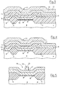
- FIG. 2 to 5 a portion of a semiconductor chip wherein the memory device of Figure 1 is integrated is shown, at an intermediate step of its manufacturing.
- thick field oxide areas 7 and thin gate oxide areas 8 are formed.
- the thick field oxide areas 7 are selectively formed over layer 6 for example by means of conventional LOCOS technique.
- the areas of the surface of layer 6 not covered by the field oxide 7 are covered by the gate oxide 8 and define the so-called "active areas" wherein the memory cells and other devices (for example MOSFETs for the circuitry external to the memory cell array) are to be formed.
- the gate oxide layer 8 is in current technology approximately 200 ⁇ thick and will form the gate oxide of both the memory cells and the MOSFETs of the circuitry.
- the field oxide 7 surrounds the area of the chip wherein the memory cell array is to be formed. Also, according to a known manufacturing process, at this step of the process substantially parallel strips of field oxide 7 are also formed inside the memory cell array area. Thus, complementary strips of gate oxide 8 are provided inside the memory matrix area between the strips of field oxide.
- the provision of strips of field oxide inside the memory cell array area is however not a limitation of the present invention: it would also be possible to form substantially rectangular areas of field oxide in the memory cell array area.
- a first layer of polysilicon 9 is formed over the whole chip surface.
- the first polysilicon layer 9 is doped with, e.g., phosphorus for reducing the resistivity thereof.
- the first polysilicon layer 9 is then selectively removed by means of a photolithographic technique for forming strips of first polysilicon layer 9 over the strips of gate oxide 8 inside the memory cell array area. Outside the memory cell array area, the first polysilicon layer 9 is not removed.
- the first polysilicon layer 9 will form the floating gates of the memory cells.
- the interpoly dielectric layer 10 can be a layer of oxide or, preferably, a composite stack of dielectric layers (e.g., Oxide-Nitride-Oxide); this is however not relevant to the invention.
- the interpoly dielectric layer 10 is then selectively etched and removed outside the memory cell array area.
- a second layer of polysilicon 11 is deposited over the whole chip.
- the second polysilicon layer 11 is doped with, e.g., phosphorus for reducing its resistivity.
- a silicide layer (not shown in the drawings for the sake of simplicity) can also be formed over the second polysilicon layer 11 for further reducing the resistivity thereof.
- the second polysilicon layer 11 is separated from the first polysilicon layer 9 by the interpoly dielectric layer 10. Outside the memory cell array, the second polysilicon layer 11 is in direct contact with the first polysilicon layer 9 (double polysilicon in short-circuit). Outside the memory cell array, the first and second polysilicon layers 9, 11 will form the gate electrodes of the MOSFETs of the circuitry.
- a photoresist layer 12 is then deposited over the whole chip.
- a photolithographic technique involving the use of a first photolithographic mask (in the following referred to as "MASK1")the photoresist layer 12 is selectively removed from over the chip surface.
- the layout of the photoresist layer 12 after it has been selectively removed is clearly visible in Figure 2. All the memory cell array area is covered by a plate of photoresist layer 12. Outside the memory cell array, over the field oxide 7 surrounding the memory cell array, photoresist strips 13 are left. The photoresist strips 13 are joined to the photoresist plate covering the memory cell array through enlarged photoresist pads 14.
- FIG. 2 there is also shown a photoresist strip 15 left over a portion of active area 16 outside the memory cell array area, wherein an N-channel MOSFET of the circuitry will be formed. Similarly, photoresist strips are left over portions of active areas outside the memory cell array wherein P-channel MOSFETs will be formed.
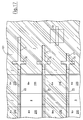
- FIG. 10 another photoresist layer 20 is subsequently deposited over the whole chip.
- the photoresist layer 20 is selectively removed from over the chip surface.
- the layout of the photoresist layer 20 after the selective removal is clearly visible in Figure 10.
- a photoresist plate covers all the chip surface outside the memory cell array area. Inside the memory cell array area photoresist strips 21 are left, which extend over the field oxide 7 surrounding the memory cell array area. The strips 21 join the photoresist plate covering all the remaining of the chip surface.
- MASK2 is such that the edge of the photoresist plate covering all the chip with the exception of the memory cell array area falls inside the enlarged pads 18 previously defined in the first and second polysilicon layers 9,11.
- Provision of the enlarged pad areas 14 is advantageous because they allow to obtain low-resistivity interconnection lines made from the second polysilicon layer 11 even in case of slight misalignment between MASK1 and MASK2.
- the strips 17 outside the memory cell array are defined before the strips 22 inside the memory cell array.
- the enlarged pad areas 18 could be formed not by means of MASK1, but by means of MASK2. It is however important that, in both cases, the enlarged pad areas 18 are formed over the field oxide 7 surrounding the memory array, and not over the active areas covered by the gate oxide layer 8, because in the latter case during the etching process the silicon layer 6 could be attacked too (as visible in Figure 10, due to the particular alignment of the masks, areas of field oxide 7 whereover the first and second polysilicon layers 9,11 were previously removed are exposed and undergo the etching process that allows to define strips 22; if said exposed areas were gate oxide areas, the thin gate oxide layer would be easily attacked and removed, and the underlying silicon layer 6 would be exposed to the etching reactants).
- an N type dopant typically arsenic
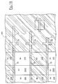
- an N type dopant is then selectively implanted in a dose of approximately 10 15 atoms/cm 2 only in the memory cell array area to form in the substrate 6 N+ source and drain regions 23S, 23D for the memory cells, aligned with the edges of the rows (i.e., strips 22) of the memory cell array. Regions 23S, 23D are formed only where the field oxide 7 is absent. Then, the photoresist layer 20 is completely removed ( Figure 16).
- photoresist layer 101 is deposited and selectively removed by means of a so-called “Self-Aligned-Source” (SAS) mask. Then, the uncovered portions of the field oxide 7 inside the memory cell array area are selectively removed where common source diffusions for the memory cells will be formed ( Figure 17).
- the photoresist layer 101 covers the circuitry and the drain regions of the memory cells and the strips 22 (rows) of the memory cell array.
- an implant of an N-type dopant, typically arsenic, in a dose of approximately 10 15 atoms/cm 2 is performed to form N+ regions 23CS which, together with source regions 23S, form common source diffusions for the memory cell array ( Figure 18).
- the photoresist layer 101 is removed, and a thermal process is performed for diffusing the arsenic atoms previously implanted.
- a low-dose implant typically 10 12 or 10 13 atoms/cm 2
- N-LDD N-type Lightly Doped Drain
- a photoresist layer is then deposited, and it is selectively removed by means of a so-called "P-LDD mask".
- P-LDD mask covers all the memory cell array area, and also the active areas (e.g., active area 16) of the circuitry where N-channel MOSFET are to be formed.
- a low dose of a P type dopant is implanted to form P-type LDD regions for the P-channel MOSFETs of the circuitry.
- the photoresist layer for the P-LDD implant is then removed.
- Insulating sidewall spacers are then conventionally formed at the sides of the gate electrodes of the MOSFETs of the circuitry (e.g., srip 19), as well as at the sides of the rows of the memory cell array (strips 22).
- a photoresist layer is then deposited, and it is selectively removed to expose the source and drain regions of the N-channel MOSFETs of the circuitry. Then, a heavy dose implant of an N-type dopant (e.g., arsenic in a dose of approximately 10 15 atoms/cm 2 ) is performed to form heavily-doped N-type (N+) source and drain regions of the N-channel MOSFETs of the circuitry. Due to the presence of the sidewall spacers, the N+ source and drain regions of the N-channel MOSFETs do not extend to the edges of the gate electrodes, and an N- source and drain region is left under the spacers. The photoresist layer is then removed, and a thermal process is performed for diffusing the implanted dopant.
- an N-type dopant e.g., arsenic in a dose of approximately 10 15 atoms/cm 2
- snother photoresist layer is then deposited, and it is selectively removed by means of a mask for exposing the source and drain regions of the P-channel MOSFETs of the circuitry.
- a heavy dose of a P-type dopant is implanted to form P+ source and drain regions for the same.
- the P+ source and drain regions do not extend to the edges of the gates, and P- source and drain regions are left under the spacers.
- the process then goes on conventionally with the deposition of a dielectric layer, the formation of contact holes therein, the formation of metal interconnection lines, and so on.
- the photoresist layer 20 is not removed after the definition of the strips 22 and the implantation of the N-type dopant for forming the N+ regions 23S, 23D.
- the photoresist layer for the SAS mask is then deposited over the photoresist layer 20, and the etching of the portions of field oxide 7 is performed. In this way, during the etching of the field oxide 7 the polysilicon strips 22 are covered by the photoresist layer 20, that protects the strips 22 from the etching reactants.
- the SAS mask normally leaves the sides of the strips 22 uncovered, so that during the etching of the field oxide 7 the strips 22 are partially etched too, and this cause an increase in the resistance of the rows of the memory cell array.
- the two masks MASK1 and MASK2 for defining the strips 17, 19 and 22 are applied sequentially, i.e. one (either MASK1 or MASK2) immediately after the other.
- the two masks MASK1 and MASK2 are not applied sequentially.
- MASK1 is applied first, and the two polysilicon layers 9,11 are selectively removed for defining the strips 17,19 in the circuitry area. Then, the photoresist layer 12 is removed.
- the low-dose implant of the N-type dopant for forming the N-LDD source and drain regions of the N-channel MOSFETs is performed before defining the strips 22 in the memory cell array area.
- the selective implant of the low dose of P-type dopant for forming the P-LDD source and drain regions for the P-channel MOSFETs is then performed.
- the memory cell array area is at this step still covered by the gate oxide layer 8, the first polysilicon layer 9, the interpoly dielectric layer 10 and the second polysilicon layer 11.
- the insulating sidewall spacers are then formed at the sides of the gate electrodes of the MOSFETs of the circuitry. No sidewall spacers are formed in the memory cell array area, which is covered by a plate of second polysilicon layer. Then, the photoresist layer 20 is deposited and MASK2 is applied for selectively removing the photoresist layer 20. The strips 22 are then defined in the memory cell array area by means of the selective etching of layers 11, 10, 9, 8.
- the photoresist layer 101 for the SAS mask is deposited and selectively removed; portions of the field oxide 7 in the memory cell array area are then etched. At this step, only the portions of the chip where the N+ regions 23S, 23CS will be formed are not covered by the photoresist layer 101. Then, MASK2 is applied and the photoresist layer 101 selectively removed for exposing also the regions of the memory cell array where the N+ drain region 23D of the memory cells will be formed. Subsequently, the mask used in the previous process for the selective formation of the N+ source and drain regions of the N-channel MOSFETs is applied.
- a high-dose implant of an N-type dopant (typically arsenic in a dose of 10 15 atoms/cm 2 ) is performed, to simultaneously form the N+ source and drain regions 23S, 23D of the memory cells, the N+ common source lines 23CS of the memory cell array, and the N+ source and drain regions of the N-channel MOSFETs. Then the remaining of the photoresist layer 101 (and, if not previously removed, the remaining of the photoresist layer 20) is removed, and a thermal process is performed for diffusing the implanted dopant.
- an N-type dopant typically arsenic in a dose of 10 15 atoms/cm 2
- a high dose of a P-type dopant is selectively implanted in the active areas for the P-channel MOSFETs of the circuitry, to form P+ source and drain for the P-channel MOSFETs.
- the process then conventionally goes on with the deposition of a dielectric layer, the formation of contact opening therein, the formation of metal interconnection lines, etc.
- this second embodiment allows for eliminating two high-dose implant of an N-type dopant and one thermal diffusion process.
- the source and drain regions 23S, 23D of the memory cells, the common source lines 23CS of the memory cell array and source and drain regions of the N-channel MOSFETs are formed by means of the same implant. Eliminating one thermal diffusion process allows for an increase in the effective length of the memory cells, so that it is possible to reduce the memory cell area.
- Another advantage of the process according to the second embodiment of the invention is the following.
- the insulating sidewall spacers are formed in the circuitry area when the memory cell array area is still covered by the second polysilicon layer, while in the first embodiment of the process the spacers are formed simultaneously in the circuitry and memory cell array areas. Formation of the sidewall spacers in the memory cell array area is not strictly necessary, but cannot be avoided in the first embodiment of the process.
- the formation of the spacers conventionally provides for forming an oxide layer over the whole chip, and then performing an etching so that the oxide layer is left only at the sides of steps. In the first embodiment of the process, etching of the oxide layer forming the spacers causes a thinning of the field oxide layer in the memory cell array area, which can cause problems.
- the second embodiment of the process instead, during etching of the oxide layer for forming the spacers the memory cell array is still covered by the second polysilicon layer, and the field oxide is not affected.
Landscapes
- Engineering & Computer Science (AREA)
- Manufacturing & Machinery (AREA)
- Semiconductor Memories (AREA)
- Non-Volatile Memory (AREA)
Priority Applications (4)
| Application Number | Priority Date | Filing Date | Title |
|---|---|---|---|
| DE69732838T DE69732838D1 (de) | 1997-07-16 | 1997-07-16 | Herstellungsverfahren für einen integrierten Schaltkreis mit einer Speicherzellenmatrix |
| EP97830359A EP0892430B1 (fr) | 1997-07-16 | 1997-07-16 | Procédé de fabrication d'un circuit intégré comprenant une matrice de cellules de mémoire |
| US08/897,799 US5976933A (en) | 1997-07-16 | 1997-07-21 | Process for manufacturing an integrated circuit comprising an array of memory cells |
| US09/356,080 US6353243B1 (en) | 1997-07-16 | 1999-07-16 | Process for manufacturing an integrated circuit comprising an array of memory cells |
Applications Claiming Priority (1)
| Application Number | Priority Date | Filing Date | Title |
|---|---|---|---|
| EP97830359A EP0892430B1 (fr) | 1997-07-16 | 1997-07-16 | Procédé de fabrication d'un circuit intégré comprenant une matrice de cellules de mémoire |
Publications (2)
| Publication Number | Publication Date |
|---|---|
| EP0892430A1 true EP0892430A1 (fr) | 1999-01-20 |
| EP0892430B1 EP0892430B1 (fr) | 2005-03-23 |
Family
ID=8230710
Family Applications (1)
| Application Number | Title | Priority Date | Filing Date |
|---|---|---|---|
| EP97830359A Expired - Lifetime EP0892430B1 (fr) | 1997-07-16 | 1997-07-16 | Procédé de fabrication d'un circuit intégré comprenant une matrice de cellules de mémoire |
Country Status (3)
| Country | Link |
|---|---|
| US (2) | US5976933A (fr) |
| EP (1) | EP0892430B1 (fr) |
| DE (1) | DE69732838D1 (fr) |
Cited By (1)
| Publication number | Priority date | Publication date | Assignee | Title |
|---|---|---|---|---|
| GB2347016A (en) * | 1999-02-17 | 2000-08-23 | Ibm | Triple polysilicon embedded NVRAM cell |
Families Citing this family (6)
| Publication number | Priority date | Publication date | Assignee | Title |
|---|---|---|---|---|
| DE69732838D1 (de) * | 1997-07-16 | 2005-04-28 | St Microelectronics Srl | Herstellungsverfahren für einen integrierten Schaltkreis mit einer Speicherzellenmatrix |
| TW484228B (en) * | 1999-08-31 | 2002-04-21 | Toshiba Corp | Non-volatile semiconductor memory device and the manufacturing method thereof |
| US6268274B1 (en) * | 1999-10-14 | 2001-07-31 | Taiwan Semiconductor Manufacturing Company | Low temperature process for forming inter-metal gap-filling insulating layers in silicon wafer integrated circuitry |
| US7786021B2 (en) * | 2002-11-14 | 2010-08-31 | Sharp Laboratories Of America, Inc. | High-density plasma multilayer gate oxide |
| US8118946B2 (en) | 2007-11-30 | 2012-02-21 | Wesley George Lau | Cleaning process residues from substrate processing chamber components |
| US11031308B2 (en) * | 2019-05-30 | 2021-06-08 | Sandisk Technologies Llc | Connectivity detection for wafer-to-wafer alignment and bonding |
Citations (3)
| Publication number | Priority date | Publication date | Assignee | Title |
|---|---|---|---|---|
| EP0379450A1 (fr) * | 1989-01-17 | 1990-07-25 | STMicroelectronics S.A. | Procédé de fabrication de circuits intégrés à transistors de mémoire EPROM et à transistors logiques |
| JPH0449675A (ja) * | 1990-06-19 | 1992-02-19 | Nec Corp | 半導体装置 |
| JPH08298314A (ja) * | 1995-04-27 | 1996-11-12 | Nec Yamaguchi Ltd | 不揮発性半導体記憶装置及びその製造方法 |
Family Cites Families (5)
| Publication number | Priority date | Publication date | Assignee | Title |
|---|---|---|---|---|
| US4453175A (en) * | 1979-09-19 | 1984-06-05 | Tokyo Shibaura Denki Kabushiki Kaisha | MOS Static RAM layout with polysilicon resistors over FET gates |
| KR940002772B1 (ko) * | 1984-08-31 | 1994-04-02 | 가부시기가이샤 히다찌세이사꾸쇼 | 반도체 집적회로 장치 및 그 제조방법 |
| JP3363502B2 (ja) * | 1993-02-01 | 2003-01-08 | 三菱電機株式会社 | 半導体記憶装置の製造方法 |
| US5716864A (en) * | 1994-07-22 | 1998-02-10 | Nkk Corporation | Method of manufacturing a non-volatile semiconductor memory device with peripheral transistor |
| DE69732838D1 (de) * | 1997-07-16 | 2005-04-28 | St Microelectronics Srl | Herstellungsverfahren für einen integrierten Schaltkreis mit einer Speicherzellenmatrix |
-
1997
- 1997-07-16 DE DE69732838T patent/DE69732838D1/de not_active Expired - Lifetime
- 1997-07-16 EP EP97830359A patent/EP0892430B1/fr not_active Expired - Lifetime
- 1997-07-21 US US08/897,799 patent/US5976933A/en not_active Expired - Lifetime
-
1999
- 1999-07-16 US US09/356,080 patent/US6353243B1/en not_active Expired - Fee Related
Patent Citations (3)
| Publication number | Priority date | Publication date | Assignee | Title |
|---|---|---|---|---|
| EP0379450A1 (fr) * | 1989-01-17 | 1990-07-25 | STMicroelectronics S.A. | Procédé de fabrication de circuits intégrés à transistors de mémoire EPROM et à transistors logiques |
| JPH0449675A (ja) * | 1990-06-19 | 1992-02-19 | Nec Corp | 半導体装置 |
| JPH08298314A (ja) * | 1995-04-27 | 1996-11-12 | Nec Yamaguchi Ltd | 不揮発性半導体記憶装置及びその製造方法 |
Non-Patent Citations (2)
| Title |
|---|
| PATENT ABSTRACTS OF JAPAN vol. 016, no. 240 (E - 1211) 3 June 1992 (1992-06-03) * |
| PATENT ABSTRACTS OF JAPAN vol. 097, no. 003 31 March 1997 (1997-03-31) * |
Cited By (4)
| Publication number | Priority date | Publication date | Assignee | Title |
|---|---|---|---|---|
| GB2347016A (en) * | 1999-02-17 | 2000-08-23 | Ibm | Triple polysilicon embedded NVRAM cell |
| US6180456B1 (en) | 1999-02-17 | 2001-01-30 | International Business Machines Corporation | Triple polysilicon embedded NVRAM cell and method thereof |
| SG83184A1 (en) * | 1999-02-17 | 2001-09-18 | Ibm | Triple polysilicon embedded nvram cell and method thereof |
| GB2347016B (en) * | 1999-02-17 | 2003-07-02 | Ibm | Triple polysilicon embedded vnram cell |
Also Published As
| Publication number | Publication date |
|---|---|
| US5976933A (en) | 1999-11-02 |
| DE69732838D1 (de) | 2005-04-28 |
| EP0892430B1 (fr) | 2005-03-23 |
| US6353243B1 (en) | 2002-03-05 |
Similar Documents
| Publication | Publication Date | Title |
|---|---|---|
| US5019527A (en) | Method of manufacturing non-volatile semiconductor memories, in which selective removal of field oxidation film for forming source region and self-adjusted treatment for forming contact portion are simultaneously performed | |
| KR100723993B1 (ko) | 반도체 메모리 장치와 그 제조 방법 | |
| US7563664B2 (en) | Semiconductor memory device equipped with memory transistor and peripheral transistor and method of manufacturing the same | |
| JP2000058800A (ja) | サリサイド接合をもつlvトランジスタ及び不揮発性メモリセルを有する電子装置及びその製造方法 | |
| JP2002164536A (ja) | 半導体装置及びその製造方法 | |
| US20010024861A1 (en) | Method for manufacturing electronic devices having HV transistors and LV transistors with salicided junctions | |
| US6673674B2 (en) | Method of manufacturing a semiconductor device having a T-shaped floating gate | |
| US20010021556A1 (en) | Method for manufacturing electronic devices comprising non-volatile memory cells and LV transistors with salicided junctions | |
| JP2945969B2 (ja) | 不揮発性メモリデバイス並びにその製造方法 | |
| US5976933A (en) | Process for manufacturing an integrated circuit comprising an array of memory cells | |
| US5506159A (en) | Method for manufacturing a semiconductor memory device | |
| US6064099A (en) | Layout of well contacts and source contacts of a semiconductor device | |
| US6380584B1 (en) | Semiconductor memory device with single and double sidewall spacers | |
| JP2000124450A5 (fr) | ||
| US6344386B1 (en) | Method for fabricating semiconductor device including memory cell region and CMOS logic region | |
| KR100251229B1 (ko) | 노아형 마스크 롬의 개선된 구조 및 그 제조방법 | |
| JP4266089B2 (ja) | 半導体記憶装置の製造方法 | |
| US6414346B1 (en) | Semiconductor memory and manufacturing method thereof | |
| US6445031B1 (en) | Byte-switch structure for EEPROM memories | |
| US20030015751A1 (en) | Semiconductor memory device including memory cells and peripheral circuits and method for manufacturing the same | |
| JPH1022404A (ja) | スプリットゲートタイプの半導体装置の製造方法 | |
| JP2001332639A (ja) | Mos型半導体記憶装置およびその製造方法 | |
| JPH08102531A (ja) | 半導体記憶装置及びその製造方法 | |
| JPH1079494A (ja) | 半導体装置及びその製造方法 | |
| JP2002289792A (ja) | 半導体装置の製造方法 |
Legal Events
| Date | Code | Title | Description |
|---|---|---|---|
| PUAI | Public reference made under article 153(3) epc to a published international application that has entered the european phase |
Free format text: ORIGINAL CODE: 0009012 |
|
| AK | Designated contracting states |
Kind code of ref document: A1 Designated state(s): DE FR GB IT |
|
| 17P | Request for examination filed |
Effective date: 19990426 |
|
| AKX | Designation fees paid |
Free format text: DE FR GB IT |
|
| 17Q | First examination report despatched |
Effective date: 20021219 |
|
| GRAP | Despatch of communication of intention to grant a patent |
Free format text: ORIGINAL CODE: EPIDOSNIGR1 |
|
| GRAS | Grant fee paid |
Free format text: ORIGINAL CODE: EPIDOSNIGR3 |
|
| GRAA | (expected) grant |
Free format text: ORIGINAL CODE: 0009210 |
|
| AK | Designated contracting states |
Kind code of ref document: B1 Designated state(s): DE FR GB IT |
|
| REG | Reference to a national code |
Ref country code: GB Ref legal event code: FG4D |
|
| REF | Corresponds to: |
Ref document number: 69732838 Country of ref document: DE Date of ref document: 20050428 Kind code of ref document: P |
|
| PG25 | Lapsed in a contracting state [announced via postgrant information from national office to epo] |
Ref country code: DE Free format text: LAPSE BECAUSE OF FAILURE TO SUBMIT A TRANSLATION OF THE DESCRIPTION OR TO PAY THE FEE WITHIN THE PRESCRIBED TIME-LIMIT Effective date: 20050624 |
|
| PLBE | No opposition filed within time limit |
Free format text: ORIGINAL CODE: 0009261 |
|
| STAA | Information on the status of an ep patent application or granted ep patent |
Free format text: STATUS: NO OPPOSITION FILED WITHIN TIME LIMIT |
|
| 26N | No opposition filed |
Effective date: 20051227 |
|
| ET | Fr: translation filed | ||
| PGFP | Annual fee paid to national office [announced via postgrant information from national office to epo] |
Ref country code: IT Payment date: 20080717 Year of fee payment: 12 Ref country code: FR Payment date: 20080730 Year of fee payment: 12 |
|
| PGFP | Annual fee paid to national office [announced via postgrant information from national office to epo] |
Ref country code: GB Payment date: 20080630 Year of fee payment: 12 |
|
| GBPC | Gb: european patent ceased through non-payment of renewal fee |
Effective date: 20090716 |
|
| REG | Reference to a national code |
Ref country code: FR Ref legal event code: ST Effective date: 20100331 |
|
| PG25 | Lapsed in a contracting state [announced via postgrant information from national office to epo] |
Ref country code: FR Free format text: LAPSE BECAUSE OF NON-PAYMENT OF DUE FEES Effective date: 20090731 |
|
| PG25 | Lapsed in a contracting state [announced via postgrant information from national office to epo] |
Ref country code: GB Free format text: LAPSE BECAUSE OF NON-PAYMENT OF DUE FEES Effective date: 20090716 |
|
| PG25 | Lapsed in a contracting state [announced via postgrant information from national office to epo] |
Ref country code: IT Free format text: LAPSE BECAUSE OF NON-PAYMENT OF DUE FEES Effective date: 20090716 |