EP0892438A2 - Relais à semi-conducteur - Google Patents
Relais à semi-conducteur Download PDFInfo
- Publication number
- EP0892438A2 EP0892438A2 EP98111987A EP98111987A EP0892438A2 EP 0892438 A2 EP0892438 A2 EP 0892438A2 EP 98111987 A EP98111987 A EP 98111987A EP 98111987 A EP98111987 A EP 98111987A EP 0892438 A2 EP0892438 A2 EP 0892438A2
- Authority
- EP
- European Patent Office
- Prior art keywords
- source
- region
- drain
- solid
- silicon layer
- Prior art date
- Legal status (The legal status is an assumption and is not a legal conclusion. Google has not performed a legal analysis and makes no representation as to the accuracy of the status listed.)
- Granted
Links
Images


Classifications
-
- H—ELECTRICITY
- H10—SEMICONDUCTOR DEVICES; ELECTRIC SOLID-STATE DEVICES NOT OTHERWISE PROVIDED FOR
- H10D—INORGANIC ELECTRIC SEMICONDUCTOR DEVICES
- H10D86/00—Integrated devices formed in or on insulating or conducting substrates, e.g. formed in silicon-on-insulator [SOI] substrates or on stainless steel or glass substrates
- H10D86/201—Integrated devices formed in or on insulating or conducting substrates, e.g. formed in silicon-on-insulator [SOI] substrates or on stainless steel or glass substrates the substrates comprising an insulating layer on a semiconductor body, e.g. SOI
-
- H—ELECTRICITY
- H10—SEMICONDUCTOR DEVICES; ELECTRIC SOLID-STATE DEVICES NOT OTHERWISE PROVIDED FOR
- H10D—INORGANIC ELECTRIC SEMICONDUCTOR DEVICES
- H10D30/00—Field-effect transistors [FET]
- H10D30/60—Insulated-gate field-effect transistors [IGFET]
- H10D30/64—Double-diffused metal-oxide semiconductor [DMOS] FETs
- H10D30/65—Lateral DMOS [LDMOS] FETs
- H10D30/657—Lateral DMOS [LDMOS] FETs having substrates comprising insulating layers, e.g. SOI-LDMOS transistors
-
- H—ELECTRICITY
- H10—SEMICONDUCTOR DEVICES; ELECTRIC SOLID-STATE DEVICES NOT OTHERWISE PROVIDED FOR
- H10D—INORGANIC ELECTRIC SEMICONDUCTOR DEVICES
- H10D62/00—Semiconductor bodies, or regions thereof, of devices having potential barriers
- H10D62/10—Shapes, relative sizes or dispositions of the regions of the semiconductor bodies; Shapes of the semiconductor bodies
- H10D62/113—Isolations within a component, i.e. internal isolations
- H10D62/115—Dielectric isolations, e.g. air gaps
- H10D62/116—Dielectric isolations, e.g. air gaps adjoining the input or output regions of field-effect devices, e.g. adjoining source or drain regions
-
- H—ELECTRICITY
- H10—SEMICONDUCTOR DEVICES; ELECTRIC SOLID-STATE DEVICES NOT OTHERWISE PROVIDED FOR
- H10D—INORGANIC ELECTRIC SEMICONDUCTOR DEVICES
- H10D62/00—Semiconductor bodies, or regions thereof, of devices having potential barriers
- H10D62/10—Shapes, relative sizes or dispositions of the regions of the semiconductor bodies; Shapes of the semiconductor bodies
- H10D62/124—Shapes, relative sizes or dispositions of the regions of semiconductor bodies or of junctions between the regions
- H10D62/126—Top-view geometrical layouts of the regions or the junctions
- H10D62/127—Top-view geometrical layouts of the regions or the junctions of cellular field-effect devices, e.g. multicellular DMOS transistors or IGBTs
-
- H—ELECTRICITY
- H10—SEMICONDUCTOR DEVICES; ELECTRIC SOLID-STATE DEVICES NOT OTHERWISE PROVIDED FOR
- H10D—INORGANIC ELECTRIC SEMICONDUCTOR DEVICES
- H10D84/00—Integrated devices formed in or on semiconductor substrates that comprise only semiconducting layers, e.g. on Si wafers or on GaAs-on-Si wafers
- H10D84/80—Integrated devices formed in or on semiconductor substrates that comprise only semiconducting layers, e.g. on Si wafers or on GaAs-on-Si wafers characterised by the integration of at least one component covered by groups H10D12/00 or H10D30/00, e.g. integration of IGFETs
- H10D84/82—Integrated devices formed in or on semiconductor substrates that comprise only semiconducting layers, e.g. on Si wafers or on GaAs-on-Si wafers characterised by the integration of at least one component covered by groups H10D12/00 or H10D30/00, e.g. integration of IGFETs of only field-effect components
- H10D84/83—Integrated devices formed in or on semiconductor substrates that comprise only semiconducting layers, e.g. on Si wafers or on GaAs-on-Si wafers characterised by the integration of at least one component covered by groups H10D12/00 or H10D30/00, e.g. integration of IGFETs of only field-effect components of only insulated-gate FETs [IGFET]
-
- H—ELECTRICITY
- H10—SEMICONDUCTOR DEVICES; ELECTRIC SOLID-STATE DEVICES NOT OTHERWISE PROVIDED FOR
- H10W—GENERIC PACKAGES, INTERCONNECTIONS, CONNECTORS OR OTHER CONSTRUCTIONAL DETAILS OF DEVICES COVERED BY CLASS H10
- H10W70/00—Package substrates; Interposers; Redistribution layers [RDL]
- H10W70/40—Leadframes
- H10W70/481—Leadframes for devices being provided for in groups H10D8/00 - H10D48/00
-
- H—ELECTRICITY
- H10—SEMICONDUCTOR DEVICES; ELECTRIC SOLID-STATE DEVICES NOT OTHERWISE PROVIDED FOR
- H10W—GENERIC PACKAGES, INTERCONNECTIONS, CONNECTORS OR OTHER CONSTRUCTIONAL DETAILS OF DEVICES COVERED BY CLASS H10
- H10W72/00—Interconnections or connectors in packages
- H10W72/90—Bond pads, in general
-
- H—ELECTRICITY
- H10—SEMICONDUCTOR DEVICES; ELECTRIC SOLID-STATE DEVICES NOT OTHERWISE PROVIDED FOR
- H10W—GENERIC PACKAGES, INTERCONNECTIONS, CONNECTORS OR OTHER CONSTRUCTIONAL DETAILS OF DEVICES COVERED BY CLASS H10
- H10W90/00—Package configurations
- H10W90/811—Multiple chips on leadframes
-
- H—ELECTRICITY
- H10—SEMICONDUCTOR DEVICES; ELECTRIC SOLID-STATE DEVICES NOT OTHERWISE PROVIDED FOR
- H10W—GENERIC PACKAGES, INTERCONNECTIONS, CONNECTORS OR OTHER CONSTRUCTIONAL DETAILS OF DEVICES COVERED BY CLASS H10
- H10W72/00—Interconnections or connectors in packages
- H10W72/50—Bond wires
-
- H—ELECTRICITY
- H10—SEMICONDUCTOR DEVICES; ELECTRIC SOLID-STATE DEVICES NOT OTHERWISE PROVIDED FOR
- H10W—GENERIC PACKAGES, INTERCONNECTIONS, CONNECTORS OR OTHER CONSTRUCTIONAL DETAILS OF DEVICES COVERED BY CLASS H10
- H10W72/00—Interconnections or connectors in packages
- H10W72/851—Dispositions of multiple connectors or interconnections
- H10W72/874—On different surfaces
- H10W72/884—Die-attach connectors and bond wires
-
- H—ELECTRICITY
- H10—SEMICONDUCTOR DEVICES; ELECTRIC SOLID-STATE DEVICES NOT OTHERWISE PROVIDED FOR
- H10W—GENERIC PACKAGES, INTERCONNECTIONS, CONNECTORS OR OTHER CONSTRUCTIONAL DETAILS OF DEVICES COVERED BY CLASS H10
- H10W72/00—Interconnections or connectors in packages
- H10W72/90—Bond pads, in general
- H10W72/931—Shapes of bond pads
- H10W72/932—Plan-view shape, i.e. in top view
-
- H—ELECTRICITY
- H10—SEMICONDUCTOR DEVICES; ELECTRIC SOLID-STATE DEVICES NOT OTHERWISE PROVIDED FOR
- H10W—GENERIC PACKAGES, INTERCONNECTIONS, CONNECTORS OR OTHER CONSTRUCTIONAL DETAILS OF DEVICES COVERED BY CLASS H10
- H10W72/00—Interconnections or connectors in packages
- H10W72/90—Bond pads, in general
- H10W72/951—Materials of bond pads
- H10W72/952—Materials of bond pads comprising metals or metalloids, e.g. PbSn, Ag or Cu
-
- H—ELECTRICITY
- H10—SEMICONDUCTOR DEVICES; ELECTRIC SOLID-STATE DEVICES NOT OTHERWISE PROVIDED FOR
- H10W—GENERIC PACKAGES, INTERCONNECTIONS, CONNECTORS OR OTHER CONSTRUCTIONAL DETAILS OF DEVICES COVERED BY CLASS H10
- H10W90/00—Package configurations
- H10W90/701—Package configurations characterised by the relative positions of pads or connectors relative to package parts
- H10W90/731—Package configurations characterised by the relative positions of pads or connectors relative to package parts of die-attach connectors
- H10W90/736—Package configurations characterised by the relative positions of pads or connectors relative to package parts of die-attach connectors between a chip and a stacked lead frame, conducting package substrate or heat sink
-
- H—ELECTRICITY
- H10—SEMICONDUCTOR DEVICES; ELECTRIC SOLID-STATE DEVICES NOT OTHERWISE PROVIDED FOR
- H10W—GENERIC PACKAGES, INTERCONNECTIONS, CONNECTORS OR OTHER CONSTRUCTIONAL DETAILS OF DEVICES COVERED BY CLASS H10
- H10W90/00—Package configurations
- H10W90/701—Package configurations characterised by the relative positions of pads or connectors relative to package parts
- H10W90/751—Package configurations characterised by the relative positions of pads or connectors relative to package parts of bond wires
- H10W90/753—Package configurations characterised by the relative positions of pads or connectors relative to package parts of bond wires between laterally-adjacent chips
-
- H—ELECTRICITY
- H10—SEMICONDUCTOR DEVICES; ELECTRIC SOLID-STATE DEVICES NOT OTHERWISE PROVIDED FOR
- H10W—GENERIC PACKAGES, INTERCONNECTIONS, CONNECTORS OR OTHER CONSTRUCTIONAL DETAILS OF DEVICES COVERED BY CLASS H10
- H10W90/00—Package configurations
- H10W90/701—Package configurations characterised by the relative positions of pads or connectors relative to package parts
- H10W90/751—Package configurations characterised by the relative positions of pads or connectors relative to package parts of bond wires
- H10W90/754—Package configurations characterised by the relative positions of pads or connectors relative to package parts of bond wires between a chip and a stacked insulating package substrate, interposer or RDL
-
- H—ELECTRICITY
- H10—SEMICONDUCTOR DEVICES; ELECTRIC SOLID-STATE DEVICES NOT OTHERWISE PROVIDED FOR
- H10W—GENERIC PACKAGES, INTERCONNECTIONS, CONNECTORS OR OTHER CONSTRUCTIONAL DETAILS OF DEVICES COVERED BY CLASS H10
- H10W90/00—Package configurations
- H10W90/701—Package configurations characterised by the relative positions of pads or connectors relative to package parts
- H10W90/751—Package configurations characterised by the relative positions of pads or connectors relative to package parts of bond wires
- H10W90/756—Package configurations characterised by the relative positions of pads or connectors relative to package parts of bond wires between a chip and a stacked lead frame, conducting package substrate or heat sink
Definitions
- the relay As the frequency of the output signal becomes higher, the relay is required to have a lower output capacitance developed across output terminals of the relay during off-periods of the output signal, i.e., the periods in which the output terminals are in non-conductive condition, in addition to minimizing on-state resistance between the output terminals during on-periods of the output signal.
- the output capacitance is the sum of a drain-source capacitance and a gate-drain capacitance at the non-conductive condition of the output terminals of the relay.
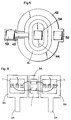
- FET is also of the SOI structure having an N-type silicon layer 10A , a buried oxide layer 20A , and a silicon substrate 30A .
- a P-type well region 11A of a closed loop configuration is diffused in the silicon layer 10A over the full depth thereof so as to leave therearound a peripheral isolated zone 16.
- a P-type source region 12A of the like closed loop configuration is diffused in the top surface of the well region 11A to define the source of FET as well as to define a channel 13A between the source region 12A and a confronting inner periphery of the well region 11A .
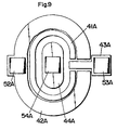
- the above illustrated embodiment discloses the configuration in which the drain region surrounded by the well region, it is equally possible to provide a configuration in which a like well region is formed centrally in the silicon layer and surrounded by a like drain region.
- a peripheral zone around the drain region is electrically connected to a like supporting plate together with the source region.
- a like separator ring may be formed around the drain region to electrically isolate the drain region from the peripheral zone.
Landscapes
- Thin Film Transistor (AREA)
- Insulated Gate Type Field-Effect Transistor (AREA)
Priority Applications (1)
| Application Number | Priority Date | Filing Date | Title |
|---|---|---|---|
| EP02005995A EP1227520B1 (fr) | 1997-06-30 | 1998-06-29 | Relais à l'état solide |
Applications Claiming Priority (12)
| Application Number | Priority Date | Filing Date | Title |
|---|---|---|---|
| JP17430697 | 1997-06-30 | ||
| JP174306/97 | 1997-06-30 | ||
| JP17430697 | 1997-06-30 | ||
| JP314036/97 | 1997-11-14 | ||
| JP31403697 | 1997-11-14 | ||
| JP314029/97 | 1997-11-14 | ||
| JP31403697 | 1997-11-14 | ||
| JP31402997A JP3319999B2 (ja) | 1997-11-14 | 1997-11-14 | 半導体スイッチ素子 |
| JP31402997 | 1997-11-14 | ||
| JP35257697 | 1997-12-22 | ||
| JP352576/97 | 1997-12-22 | ||
| JP35257697A JP3513851B2 (ja) | 1997-12-22 | 1997-12-22 | 半導体装置 |
Related Child Applications (1)
| Application Number | Title | Priority Date | Filing Date |
|---|---|---|---|
| EP02005995A Division EP1227520B1 (fr) | 1997-06-30 | 1998-06-29 | Relais à l'état solide |
Publications (3)
| Publication Number | Publication Date |
|---|---|
| EP0892438A2 true EP0892438A2 (fr) | 1999-01-20 |
| EP0892438A3 EP0892438A3 (fr) | 2000-09-13 |
| EP0892438B1 EP0892438B1 (fr) | 2007-12-05 |
Family
ID=27474558
Family Applications (2)
| Application Number | Title | Priority Date | Filing Date |
|---|---|---|---|
| EP98111987A Expired - Lifetime EP0892438B1 (fr) | 1997-06-30 | 1998-06-29 | Relais à état solide |
| EP02005995A Expired - Lifetime EP1227520B1 (fr) | 1997-06-30 | 1998-06-29 | Relais à l'état solide |
Family Applications After (1)
| Application Number | Title | Priority Date | Filing Date |
|---|---|---|---|
| EP02005995A Expired - Lifetime EP1227520B1 (fr) | 1997-06-30 | 1998-06-29 | Relais à l'état solide |
Country Status (9)
| Country | Link |
|---|---|
| US (3) | US6211551B1 (fr) |
| EP (2) | EP0892438B1 (fr) |
| KR (1) | KR100310479B1 (fr) |
| CN (1) | CN1156978C (fr) |
| CA (1) | CA2241765C (fr) |
| DE (2) | DE69838805T2 (fr) |
| MY (2) | MY118511A (fr) |
| SG (1) | SG67518A1 (fr) |
| TW (1) | TW386313B (fr) |
Cited By (1)
| Publication number | Priority date | Publication date | Assignee | Title |
|---|---|---|---|---|
| WO2007096210A1 (fr) * | 2006-02-22 | 2007-08-30 | Robert Bosch Gmbh | Procede et disposition en circuit pour la simulation d'etats d'erreur dans un appareil de commande |
Families Citing this family (27)
| Publication number | Priority date | Publication date | Assignee | Title |
|---|---|---|---|---|
| SE9901575L (sv) * | 1999-05-03 | 2000-11-04 | Eklund Klas Haakan | Halvledarelement |
| KR100751100B1 (ko) * | 1999-09-16 | 2007-08-22 | 코닌클리즈케 필립스 일렉트로닉스 엔.브이. | 반도체 디바이스 |
| US6552396B1 (en) * | 2000-03-14 | 2003-04-22 | International Business Machines Corporation | Matched transistors and methods for forming the same |
| US6614054B1 (en) * | 2000-11-27 | 2003-09-02 | Lg.Philips Lcd Co., Ltd. | Polysilicon thin film transistor used in a liquid crystal display and the fabricating method |
| JP2003101017A (ja) * | 2001-09-27 | 2003-04-04 | Mitsubishi Electric Corp | 半導体装置 |
| US6919236B2 (en) * | 2002-03-21 | 2005-07-19 | Advanced Micro Devices, Inc. | Biased, triple-well fully depleted SOI structure, and various methods of making and operating same |
| DE10227310A1 (de) * | 2002-06-19 | 2004-01-15 | Siemens Ag | Halbleiter-Schaltvorrichtung |
| CN100539184C (zh) * | 2004-02-16 | 2009-09-09 | 富士电机电子技术株式会社 | 双方向元件及其制造方法、半导体装置 |
| JP5157164B2 (ja) * | 2006-05-29 | 2013-03-06 | 富士電機株式会社 | 半導体装置、バッテリー保護回路およびバッテリーパック |
| JP2008085188A (ja) * | 2006-09-28 | 2008-04-10 | Sanyo Electric Co Ltd | 絶縁ゲート型半導体装置 |
| JP5511124B2 (ja) * | 2006-09-28 | 2014-06-04 | セミコンダクター・コンポーネンツ・インダストリーズ・リミテッド・ライアビリティ・カンパニー | 絶縁ゲート型半導体装置 |
| KR100840667B1 (ko) * | 2007-06-26 | 2008-06-24 | 주식회사 동부하이텍 | 수평형 디모스 소자 및 그 제조방법 |
| JP5337470B2 (ja) * | 2008-04-21 | 2013-11-06 | セミコンダクター・コンポーネンツ・インダストリーズ・リミテッド・ライアビリティ・カンパニー | 絶縁ゲート型半導体装置 |
| JP2010010256A (ja) * | 2008-06-25 | 2010-01-14 | Panasonic Electric Works Co Ltd | 半導体装置 |
| US20100127392A1 (en) * | 2008-11-25 | 2010-05-27 | Joe Yang | Semiconductor die |
| US8319255B2 (en) * | 2010-04-01 | 2012-11-27 | Texas Instruments Incorporated | Low side Zener reference voltage extended drain SCR clamps |
| US8524548B2 (en) * | 2011-04-26 | 2013-09-03 | National Semiconductor Corporation | DMOS Transistor with a cavity that lies below the drift region |
| JP5801713B2 (ja) | 2011-12-28 | 2015-10-28 | 株式会社ソシオネクスト | 半導体装置とその製造方法、およびcanシステム |
| EP2869339B1 (fr) * | 2013-10-31 | 2016-07-27 | Ampleon Netherlands B.V. | Agencement de transistor |
| CN103915505A (zh) * | 2014-04-21 | 2014-07-09 | 天津理工大学 | 一种槽栅槽源soi ldmos器件 |
| CN105374883B (zh) * | 2014-08-28 | 2018-06-08 | 旺宏电子股份有限公司 | 高压元件及其制造方法 |
| US9455339B2 (en) * | 2014-09-09 | 2016-09-27 | Macronix International Co., Ltd. | High voltage device and method for manufacturing the same |
| US9859225B2 (en) * | 2015-05-15 | 2018-01-02 | Skyworks Solutions, Inc. | Backside cavity formation in semiconductor devices |
| US9899527B2 (en) * | 2015-12-31 | 2018-02-20 | Globalfoundries Singapore Pte. Ltd. | Integrated circuits with gaps |
| GB2553822B (en) * | 2016-09-15 | 2018-12-26 | Murata Manufacturing Co | DC-DC Converter device |
| TWI829371B (zh) * | 2022-09-29 | 2024-01-11 | 車王電子股份有限公司 | 固態繼電器 |
| CN120882054A (zh) * | 2024-04-18 | 2025-10-31 | 东南大学 | 绝缘体上硅半导体结构及其制造方法 |
Family Cites Families (21)
| Publication number | Priority date | Publication date | Assignee | Title |
|---|---|---|---|---|
| JPS63278375A (ja) * | 1987-05-11 | 1988-11-16 | Nec Corp | 半導体集積回路装置 |
| US4864126A (en) | 1988-06-17 | 1989-09-05 | Hewlett-Packard Company | Solid state relay with optically controlled shunt and series enhancement circuit |
| DE4042334C2 (de) | 1990-02-27 | 1993-11-18 | Fraunhofer Ges Forschung | Verfahren zum Erzeugen einer isolierten, einkristallinen Siliziuminsel |
| GB2243485A (en) | 1990-04-27 | 1991-10-30 | Motorola Gmbh | Semiconductor device contact pads |
| US5126827A (en) * | 1991-01-17 | 1992-06-30 | Avantek, Inc. | Semiconductor chip header having particular surface metallization |
| US5138177A (en) * | 1991-03-26 | 1992-08-11 | At&T Bell Laboratories | Solid-state relay |
| JP2654268B2 (ja) * | 1991-05-13 | 1997-09-17 | 株式会社東芝 | 半導体装置の使用方法 |
| DE4129835A1 (de) | 1991-09-07 | 1993-03-11 | Bosch Gmbh Robert | Leistungselektroniksubstrat und verfahren zu dessen herstellung |
| US5286995A (en) * | 1992-07-14 | 1994-02-15 | Texas Instruments Incorporated | Isolated resurf LDMOS devices for multiple outputs on one die |
| JPH06268247A (ja) * | 1993-03-15 | 1994-09-22 | Matsushita Electric Works Ltd | 光結合型半導体リレー |
| US5378912A (en) * | 1993-11-10 | 1995-01-03 | Philips Electronics North America Corporation | Lateral semiconductor-on-insulator (SOI) semiconductor device having a lateral drift region |
| US5382818A (en) * | 1993-12-08 | 1995-01-17 | Philips Electronics North America Corporation | Lateral semiconductor-on-insulator (SOI) semiconductor device having a buried diode |
| JPH07211911A (ja) | 1994-01-19 | 1995-08-11 | Nippon Telegr & Teleph Corp <Ntt> | 絶縁ゲート型電界効果トランジスタ |
| US5874768A (en) * | 1994-06-15 | 1999-02-23 | Nippondenso Co., Ltd. | Semiconductor device having a high breakdown voltage |
| JPH08335684A (ja) * | 1995-06-08 | 1996-12-17 | Toshiba Corp | 半導体装置 |
| US5828112A (en) * | 1995-09-18 | 1998-10-27 | Kabushiki Kaisha Toshiba | Semiconductor device incorporating an output element having a current-detecting section |
| TW360982B (en) * | 1996-01-26 | 1999-06-11 | Matsushita Electric Works Ltd | Thin film transistor of silicon-on-insulator type |
| JP3575908B2 (ja) * | 1996-03-28 | 2004-10-13 | 株式会社東芝 | 半導体装置 |
| JP3082189B2 (ja) | 1996-05-22 | 2000-08-28 | 横河電機株式会社 | 半導体リレー |
| US5760473A (en) * | 1996-06-25 | 1998-06-02 | Brush Wellman Inc. | Semiconductor package having a eutectic bonding layer |
| US5981983A (en) * | 1996-09-18 | 1999-11-09 | Kabushiki Kaisha Toshiba | High voltage semiconductor device |
-
1998
- 1998-06-26 SG SG1998001526A patent/SG67518A1/en unknown
- 1998-06-26 US US09/105,464 patent/US6211551B1/en not_active Expired - Lifetime
- 1998-06-26 CA CA002241765A patent/CA2241765C/fr not_active Expired - Fee Related
- 1998-06-29 TW TW087110440A patent/TW386313B/zh not_active IP Right Cessation
- 1998-06-29 DE DE69838805T patent/DE69838805T2/de not_active Expired - Lifetime
- 1998-06-29 EP EP98111987A patent/EP0892438B1/fr not_active Expired - Lifetime
- 1998-06-29 EP EP02005995A patent/EP1227520B1/fr not_active Expired - Lifetime
- 1998-06-29 DE DE69840077T patent/DE69840077D1/de not_active Expired - Lifetime
- 1998-06-30 MY MYPI98002980A patent/MY118511A/en unknown
- 1998-06-30 KR KR1019980025687A patent/KR100310479B1/ko not_active Expired - Fee Related
- 1998-06-30 MY MYPI20022455A patent/MY130491A/en unknown
- 1998-06-30 CN CNB981026826A patent/CN1156978C/zh not_active Expired - Fee Related
-
2000
- 2000-11-13 US US09/709,582 patent/US6580126B1/en not_active Expired - Fee Related
- 2000-11-13 US US09/709,528 patent/US6373101B1/en not_active Expired - Fee Related
Cited By (2)
| Publication number | Priority date | Publication date | Assignee | Title |
|---|---|---|---|---|
| WO2007096210A1 (fr) * | 2006-02-22 | 2007-08-30 | Robert Bosch Gmbh | Procede et disposition en circuit pour la simulation d'etats d'erreur dans un appareil de commande |
| US8589139B2 (en) | 2006-02-22 | 2013-11-19 | Robert Bosch Gmbh | Method and circuit configuration for simulating fault states in a control unit |
Also Published As
| Publication number | Publication date |
|---|---|
| CA2241765C (fr) | 2001-08-28 |
| EP1227520A2 (fr) | 2002-07-31 |
| CN1222789A (zh) | 1999-07-14 |
| EP0892438A3 (fr) | 2000-09-13 |
| MY130491A (en) | 2007-06-29 |
| KR19990007497A (ko) | 1999-01-25 |
| US6580126B1 (en) | 2003-06-17 |
| MY118511A (en) | 2004-11-30 |
| US6211551B1 (en) | 2001-04-03 |
| EP1227520B1 (fr) | 2008-10-01 |
| DE69838805D1 (de) | 2008-01-17 |
| DE69838805T2 (de) | 2008-03-20 |
| DE69840077D1 (de) | 2008-11-13 |
| CA2241765A1 (fr) | 1998-12-30 |
| KR100310479B1 (ko) | 2001-11-30 |
| TW386313B (en) | 2000-04-01 |
| EP1227520A3 (fr) | 2003-06-18 |
| EP0892438B1 (fr) | 2007-12-05 |
| US6373101B1 (en) | 2002-04-16 |
| SG67518A1 (en) | 1999-09-21 |
| CN1156978C (zh) | 2004-07-07 |
Similar Documents
| Publication | Publication Date | Title |
|---|---|---|
| CA2241765C (fr) | Relais a semi-conducteur | |
| US6573144B2 (en) | Method for manufacturing a semiconductor device having lateral MOSFET (LDMOS) | |
| US6130458A (en) | Power IC having SOI structure | |
| TWI505444B (zh) | Semiconductor device | |
| KR100643831B1 (ko) | 반도체 장치 | |
| KR20010015835A (ko) | 반도체 장치 | |
| US20120161128A1 (en) | Die package | |
| US12342573B2 (en) | Semiconductor device | |
| JP2003007843A (ja) | 半導体装置 | |
| US7427792B2 (en) | Power transistor including a leadframe and a semiconductor chip arranged on the leadframe | |
| JP3509552B2 (ja) | 半導体装置 | |
| CN108233910B (zh) | 电子电路 | |
| US20040129864A1 (en) | Photovoltaic solid state relay | |
| US8502307B2 (en) | Vertical power semiconductor carrier having laterally isolated circuit areas | |
| KR20140131378A (ko) | 파워 전계 효과 트랜지스터 | |
| JP4447768B2 (ja) | フィールドmosトランジスタおよびそれを含む半導体集積回路 | |
| EP0323843A2 (fr) | Dispositif de puissance à semi-conducteur, vertical avec plusieurs sorties | |
| US6809393B1 (en) | Level shifter | |
| KR100312467B1 (ko) | 반도체집적회로장치 | |
| JP3142749B2 (ja) | 半導体装置 | |
| JP3513851B2 (ja) | 半導体装置 | |
| JPH104143A (ja) | 半導体集積回路 | |
| JP2001168336A (ja) | 低容量mosfetおよびこれを用いた半導体リレー装置 | |
| JPH0661478A (ja) | 半導体装置 | |
| JP2001244422A (ja) | 半導体装置 |
Legal Events
| Date | Code | Title | Description |
|---|---|---|---|
| PUAI | Public reference made under article 153(3) epc to a published international application that has entered the european phase |
Free format text: ORIGINAL CODE: 0009012 |
|
| AK | Designated contracting states |
Kind code of ref document: A2 Designated state(s): DE FR GB IT NL |
|
| AX | Request for extension of the european patent |
Free format text: AL;LT;LV;MK;RO;SI |
|
| PUAL | Search report despatched |
Free format text: ORIGINAL CODE: 0009013 |
|
| RIC1 | Information provided on ipc code assigned before grant |
Free format text: 7H 01L 27/12 A, 7H 01L 27/088 B, 7H 03K 17/785 B |
|
| AK | Designated contracting states |
Kind code of ref document: A3 Designated state(s): AT BE CH CY DE DK ES FI FR GB GR IE IT LI LU MC NL PT SE |
|
| AX | Request for extension of the european patent |
Free format text: AL;LT;LV;MK;RO;SI |
|
| 17P | Request for examination filed |
Effective date: 20001023 |
|
| AKX | Designation fees paid |
Free format text: DE FR GB IT NL |
|
| 17Q | First examination report despatched |
Effective date: 20011026 |
|
| RIN1 | Information on inventor provided before grant (corrected) |
Inventor name: MIYAMOTO, YASUNORI Inventor name: YOSHIDA, TAKESHI Inventor name: SHIRAI, YOSHIFUMI Inventor name: HAYASAKI, YOSHIKI Inventor name: KISHIDA, TAKASHI Inventor name: SUZUKI, YUJI Inventor name: TAKANO, HITOMICHI Inventor name: SUZUMURA, MASAHIKO |
|
| 17Q | First examination report despatched |
Effective date: 20011026 |
|
| RIC1 | Information provided on ipc code assigned before grant |
Ipc: H03K 17/785 20060101ALI20070427BHEP Ipc: H01L 27/088 20060101ALI20070427BHEP Ipc: H01L 27/12 20060101ALI20070427BHEP Ipc: H01L 29/06 20060101ALI20070427BHEP Ipc: H01L 29/78 20060101AFI20070427BHEP |
|
| GRAP | Despatch of communication of intention to grant a patent |
Free format text: ORIGINAL CODE: EPIDOSNIGR1 |
|
| GRAS | Grant fee paid |
Free format text: ORIGINAL CODE: EPIDOSNIGR3 |
|
| GRAA | (expected) grant |
Free format text: ORIGINAL CODE: 0009210 |
|
| AK | Designated contracting states |
Kind code of ref document: B1 Designated state(s): DE FR GB IT NL |
|
| REG | Reference to a national code |
Ref country code: GB Ref legal event code: FG4D |
|
| REF | Corresponds to: |
Ref document number: 69838805 Country of ref document: DE Date of ref document: 20080117 Kind code of ref document: P |
|
| ET | Fr: translation filed | ||
| PLBE | No opposition filed within time limit |
Free format text: ORIGINAL CODE: 0009261 |
|
| STAA | Information on the status of an ep patent application or granted ep patent |
Free format text: STATUS: NO OPPOSITION FILED WITHIN TIME LIMIT |
|
| 26N | No opposition filed |
Effective date: 20080908 |
|
| PGFP | Annual fee paid to national office [announced via postgrant information from national office to epo] |
Ref country code: NL Payment date: 20120626 Year of fee payment: 15 Ref country code: DE Payment date: 20120627 Year of fee payment: 15 |
|
| PGFP | Annual fee paid to national office [announced via postgrant information from national office to epo] |
Ref country code: FR Payment date: 20120619 Year of fee payment: 15 Ref country code: GB Payment date: 20120627 Year of fee payment: 15 |
|
| PGFP | Annual fee paid to national office [announced via postgrant information from national office to epo] |
Ref country code: IT Payment date: 20120619 Year of fee payment: 15 |
|
| REG | Reference to a national code |
Ref country code: NL Ref legal event code: V1 Effective date: 20140101 |
|
| GBPC | Gb: european patent ceased through non-payment of renewal fee |
Effective date: 20130629 |
|
| REG | Reference to a national code |
Ref country code: DE Ref legal event code: R119 Ref document number: 69838805 Country of ref document: DE Effective date: 20140101 |
|
| REG | Reference to a national code |
Ref country code: FR Ref legal event code: ST Effective date: 20140228 |
|
| PG25 | Lapsed in a contracting state [announced via postgrant information from national office to epo] |
Ref country code: DE Free format text: LAPSE BECAUSE OF NON-PAYMENT OF DUE FEES Effective date: 20140101 Ref country code: GB Free format text: LAPSE BECAUSE OF NON-PAYMENT OF DUE FEES Effective date: 20130629 Ref country code: NL Free format text: LAPSE BECAUSE OF NON-PAYMENT OF DUE FEES Effective date: 20140101 |
|
| PG25 | Lapsed in a contracting state [announced via postgrant information from national office to epo] |
Ref country code: IT Free format text: LAPSE BECAUSE OF NON-PAYMENT OF DUE FEES Effective date: 20130629 Ref country code: FR Free format text: LAPSE BECAUSE OF NON-PAYMENT OF DUE FEES Effective date: 20130701 |