EP0897128A1 - Optische vorrichtung und deren herstellungsverfahren - Google Patents
Optische vorrichtung und deren herstellungsverfahren Download PDFInfo
- Publication number
- EP0897128A1 EP0897128A1 EP98901077A EP98901077A EP0897128A1 EP 0897128 A1 EP0897128 A1 EP 0897128A1 EP 98901077 A EP98901077 A EP 98901077A EP 98901077 A EP98901077 A EP 98901077A EP 0897128 A1 EP0897128 A1 EP 0897128A1
- Authority
- EP
- European Patent Office
- Prior art keywords
- silver
- electrodes
- optical apparatus
- transparent
- conductive particles
- Prior art date
- Legal status (The legal status is an assumption and is not a legal conclusion. Google has not performed a legal analysis and makes no representation as to the accuracy of the status listed.)
- Withdrawn
Links
Images






Classifications
-
- G—PHYSICS
- G09—EDUCATION; CRYPTOGRAPHY; DISPLAY; ADVERTISING; SEALS
- G09G—ARRANGEMENTS OR CIRCUITS FOR CONTROL OF INDICATING DEVICES USING STATIC MEANS TO PRESENT VARIABLE INFORMATION
- G09G3/00—Control arrangements or circuits, of interest only in connection with visual indicators other than cathode-ray tubes
- G09G3/20—Control arrangements or circuits, of interest only in connection with visual indicators other than cathode-ray tubes for presentation of an assembly of a number of characters, e.g. a page, by composing the assembly by combination of individual elements arranged in a matrix no fixed position being assigned to or needed to be assigned to the individual characters or partial characters
- G09G3/34—Control arrangements or circuits, of interest only in connection with visual indicators other than cathode-ray tubes for presentation of an assembly of a number of characters, e.g. a page, by composing the assembly by combination of individual elements arranged in a matrix no fixed position being assigned to or needed to be assigned to the individual characters or partial characters by control of light from an independent source
- G09G3/38—Control arrangements or circuits, of interest only in connection with visual indicators other than cathode-ray tubes for presentation of an assembly of a number of characters, e.g. a page, by composing the assembly by combination of individual elements arranged in a matrix no fixed position being assigned to or needed to be assigned to the individual characters or partial characters by control of light from an independent source using electrochromic devices
-
- G—PHYSICS
- G02—OPTICS
- G02F—OPTICAL DEVICES OR ARRANGEMENTS FOR THE CONTROL OF LIGHT BY MODIFICATION OF THE OPTICAL PROPERTIES OF THE MEDIA OF THE ELEMENTS INVOLVED THEREIN; NON-LINEAR OPTICS; FREQUENCY-CHANGING OF LIGHT; OPTICAL LOGIC ELEMENTS; OPTICAL ANALOGUE/DIGITAL CONVERTERS
- G02F1/00—Devices or arrangements for the control of the intensity, colour, phase, polarisation or direction of light arriving from an independent light source, e.g. switching, gating or modulating; Non-linear optics
- G02F1/01—Devices or arrangements for the control of the intensity, colour, phase, polarisation or direction of light arriving from an independent light source, e.g. switching, gating or modulating; Non-linear optics for the control of the intensity, phase, polarisation or colour
- G02F1/15—Devices or arrangements for the control of the intensity, colour, phase, polarisation or direction of light arriving from an independent light source, e.g. switching, gating or modulating; Non-linear optics for the control of the intensity, phase, polarisation or colour based on an electrochromic effect
- G02F1/1506—Devices or arrangements for the control of the intensity, colour, phase, polarisation or direction of light arriving from an independent light source, e.g. switching, gating or modulating; Non-linear optics for the control of the intensity, phase, polarisation or colour based on an electrochromic effect caused by electrodeposition, e.g. electrolytic deposition of an inorganic material on or close to an electrode
-
- G—PHYSICS
- G02—OPTICS
- G02F—OPTICAL DEVICES OR ARRANGEMENTS FOR THE CONTROL OF LIGHT BY MODIFICATION OF THE OPTICAL PROPERTIES OF THE MEDIA OF THE ELEMENTS INVOLVED THEREIN; NON-LINEAR OPTICS; FREQUENCY-CHANGING OF LIGHT; OPTICAL LOGIC ELEMENTS; OPTICAL ANALOGUE/DIGITAL CONVERTERS
- G02F1/00—Devices or arrangements for the control of the intensity, colour, phase, polarisation or direction of light arriving from an independent light source, e.g. switching, gating or modulating; Non-linear optics
- G02F1/01—Devices or arrangements for the control of the intensity, colour, phase, polarisation or direction of light arriving from an independent light source, e.g. switching, gating or modulating; Non-linear optics for the control of the intensity, phase, polarisation or colour
- G02F1/15—Devices or arrangements for the control of the intensity, colour, phase, polarisation or direction of light arriving from an independent light source, e.g. switching, gating or modulating; Non-linear optics for the control of the intensity, phase, polarisation or colour based on an electrochromic effect
- G02F1/153—Constructional details
- G02F1/155—Electrodes
-
- G—PHYSICS
- G02—OPTICS
- G02F—OPTICAL DEVICES OR ARRANGEMENTS FOR THE CONTROL OF LIGHT BY MODIFICATION OF THE OPTICAL PROPERTIES OF THE MEDIA OF THE ELEMENTS INVOLVED THEREIN; NON-LINEAR OPTICS; FREQUENCY-CHANGING OF LIGHT; OPTICAL LOGIC ELEMENTS; OPTICAL ANALOGUE/DIGITAL CONVERTERS
- G02F2201/00—Constructional arrangements not provided for in groups G02F1/00 - G02F7/00
- G02F2201/12—Constructional arrangements not provided for in groups G02F1/00 - G02F7/00 electrode
- G02F2201/121—Constructional arrangements not provided for in groups G02F1/00 - G02F7/00 electrode common or background
Definitions
- an electrochromic device which has been employed in a digital clock or the like is a non-luminous display unit using reflected light or transmitted light. Therefore, an advantage can be obtained in that fatigue can be prevented even if observation is performed for a long time. Moreover, advantages can be obtained in that a relatively low operating voltage is required and power consumption can be reduced.
- a liquid ECD disclosed in Japanese Patent Laid-Open No. 59-24879 has been known, the foregoing liquid ECD being composed of an EC material which is an organic viologen molecule derivative which reversibly realizes a coloring/decoloring state.
- the ECD composed of the viologen molecule derivative has a problem of unsatisfactorily low response speed and an insufficient shielding characteristic.
- FIGS. 13 and 14 show the structure of a cell of the foregoing conventional electrochemical dimmer.
- a pair of transparent glass substrates 24 and 25 serving as display windows are disposed apart from each other for a predetermined distance.
- opposite working electrodes 22 and 23 made of ITO Indium Tin Oxide prepared by doping tin into indium oxide
- Silver-salt solution 21 is placed between the opposite working electrodes 22 and 23.
- Reference numeral 26 represents a counter electrode in the form of a silver plate disposed between the outer peripheries of the substrates 24 and 25 and also serving as a spacer.
- the silver-salt solution 21 is prepared by dissolving silver bromide in dimethyl sulfoxide (DMSO).
- DMSO dimethyl sulfoxide
- the counter electrode 26 is disposed as an anode and the working electrodes 22 and 23 are disposed as a cathode.
- a DC operating voltage is applied to a position between the two electrodes for a predetermined time, the following oxidation-reduction reactions occur on the cathode: Ag + + e - ⁇ Ag
- FIG. 13B is a diagram showing the principle of the above-mentioned phenomenon.
- FIGS. 15 and 16 show another electrochemical dimming device.
- a pair of transparent glass substrates 4 and 5 forming a cell are disposed apart from each other for a predetermined distance as shown in FIG. 15 which is a cross sectional view.
- Pairs of working electrode 2a, 2b, 2c, 2d and 2e and 3a, 3b, 3c, 3d and 3e each of which is made of ITO and which are disposed opposite to one another are formed on the inner surfaces of the substrates 4 and 5.
- Counter electrodes 7a and 7b in the form of silver plates are disposed on the outer peripheries of the working electrodes 2a to 2e and 3a to 3e.
- the substrates 4 and 5 are disposed apart from each other for a predetermined distance by a spacer 6. Silver-salt solution 1 is enclosed between the substrates 4 and 5.
- the working electrodes 2a to 2e and 3a to 3e and the counter electrodes 7a and 7b are formed into a concentric pattern.
- the electrodes 2a and 3a, 2b and 3b, 2c and 3c, 2d and 3d, 2e and 3e and 7a and 7b are connected to operating power sources 8a, 8b, 8c, 8d, 8e and 8f through electric lines 9a, 9b, 9c, 9d, 9e and 9f in the form of thin chrome wires.
- V 1 , V 2 , V 3 , V 4 and V 5 , while V 6 is a referential potential at the counter electrodes 7a and 7b are applied between opposite working electrodes 2a and 3a, 2b and 3b, 2c and 3c, 2d and 3d and 2e and 3e, silver can be deposited from the silver-salt solution 1 on each electrode which is the cathode.
- the transmittance of visible light is changed in accordance with the level of the voltage or time for which the voltage is applied.
- the above-mentioned electrochemical dimming device has a problem that the cost cannot be reduced because raw metal plates, such as the raw silver plates, are employed as it is to serve as the counter electrodes, 7a, 7b and 26. Since the lifetime of the device has been enlarged, there arises another problem in that silver particles inactivated and deposited on the counter electrode float in the silver-salt solution. Thus, the inside portion of the device is contaminated, causing the transmittance, which is realized when the device is in the transparent state, to deteriorate. Moreover, the electrodes are short-circuited.
- An object of the present invention is to provide an optical apparatus, such as an electrochemical dimming device, having a structure which enables the counter electrode of the electrochemical dimming device using deposition/dissolution reactions of silver to be made of a relatively low-cost material and which is able to prevent formation of inactive silver particles on the counter electrode, and a manufacturing method therefor.
- Another object of the present invention is to provide an optical apparatus which is capable of stabilizing the potential of the counter electrode and thus stably operating, and a manufacturing method therefor.
- An optical apparatus comprises: a pair of electrodes; silver-salt solution placed in contact with the pair of electrodes at a position between the pair of electrodes, wherein at least the surface of either of the pair of electrodes contains at least one type of conductive particles and at least one type of a binder.
- a method which comprises the step of: printing or applying a mixture containing at least one type of conductive particles and at least one type of binder so that at least the surface of either of the pair of electrodes is formed.
- An optical apparatus comprises: a pair of electrodes; and silver-salt solution placed in contact with the pair of electrodes between the pair of electrodes, wherein at least the surface of either of the pair of electrodes is formed by sintering at least one type of conductive particles.
- the present invention has the structure that at least the surface of the electrode of an optical device, such as an electrochemical dimming device, using deposition/dissolution of silver is formed by the mixture of the conductive particles and the binder or the material obtained by sintering the conductive particles. Therefore, the cost of the material of the electrodes can be reduced as compared with the structure in which the overall body of the electrodes are made of metal plates or the like.
- the counter electrode can be made to be substantially free from edges, local concentration of electric fields on the counter electrode can be relaxed. As a result, deposition of inactive and granular silver on the counter electrode can be reduced or prevented. As a result, floating of the inactive silver particles in the silver-salt solution which causes the transparency of the device to deteriorate and shortcut to take between the electrodes can be prevented.
- a first optical apparatus according to the present invention and a manufacturing method therefor has the structure that conductive particles are made of at least one type of a material selected from a group consisting of silver and carbon materials.
- a binder is made of one type of resin selected from a group consisting of natural rubber resin, cellulose resin, phenol resin, urethane resin and epoxy resin. It is preferable that at least the surface of either of the electrodes is formed by silver particles, the conductive particles and the binder. It is preferable that at least the surface of either of the electrodes is formed by printing or applying a mixture of the above-mentioned materials.
- the silver particles are added at a weight ratio of 0.01 time to 100 times a component composed of the conductive particles except for the silver particles and the binder to stabilize the potential of either of the electrodes and to easily prepare the mixture. It is preferable that the quantity of addition is 0.05 time to 10 times (which is applied hereinafter).
- the silver particles are added at a weight ratio of 0.01 time to 100 times (more preferably, 0.05 time to 10 times) the solid component of paste composed of the conductive particles except for the silver particles and the binder.
- the optical apparatus has the structure that the counter electrode (either of the electrodes) is made of a material obtained by causing the conductive particles to be contained in the binder.
- the cost can be reduced, the transparency of the device can be improved and occurrence between the electrodes can be prevented.
- the spectral characteristics which are considered to be determined in accordance with the operating voltage for the device it can be considered that the spectral characteristics can be improved when the material of the counter electrode is changed.
- the counter electrode is formed by causing the conductive particles to be contained in the binder or the conductive particles are sintered, silver is introduced into the counter electrode during the operation. Thus, a potential different from that of the silver plate is realized. Since the counter electrode is made of a material which is chemically instable (since silver is deposited and the composition of the counter electrode is therefore changed), control and operation sometimes encounter difficulty.
- the potential of the electrode can be stabilized.
- the silver particles are added to the paste composed of the conductive particles and the binder in a state in which the potential of either of the electrodes is different from that of the silver electrode by a positive value or a negative value of 50 mV or more, a satisfactory effect can be obtained. If the potential of either of the electrodes is different from that of the silver electrode by
- At least the surface of either of the electrodes may be formed by the conductive particles except for silver used in silver plating or silver evaporation and the binder.
- the surface may be formed by printing or applying the obtained mixture.
- silver which is plated or evaporated is added at a weight ratio of 0.01 time to 100 times (more preferably 0.05 time to 10 times) the component composed of the conductive particles except for silver and the binder because of the above-mentioned reason.
- silver which is plated or evaporated is added at a weight ratio of 0.01 time to 100 times (more preferably 0.05 time to 10 times) the solid component of paste composed of the conductive particles except for silver and the binder.
- At least the surface of either of the electrodes is formed by printing or applying paste obtained by mixing the silver-plated or silver-evaporated conductive material except for silver with the binder after the conductive material has been pulverized.
- the conductive particles plated with silver or evaporated with silver is added to the binder when the potential of either of the electrodes is different from the potential of the silver electrode by a positive value or a negative value of 50 mV or greater.
- the second optical apparatus according to the present invention has the structure that the conductive particles are made of one type of a material selected from a group consisting of silver and carbon materials.
- At least the surface of either of the electrodes is formed by a sintered layer composed of silver particles and the conductive particles except for silver. Moreover, it is preferable that the sintered layer is formed when the potential of either of the electrodes is different from the potential of the silver electrode by a positive value or a negative value of 50 mV or greater.
- At least the surface of either of the electrodes may be formed by a sintered layer composed of the silver-plated or silver evaporated conductive particles except for silver.
- At least either of the electrodes may be formed by previously forming the silver-plated or silver-evaporated conductive material except for sintered layer after the conductive material has been pulverized and by sintering the conductive material.
- the conductive material is sintered after the conductive material has been pulverized and previously molded in a case where the potential of either of the electrodes is different from the potential of the silver electrode by a positive value or a negative value of 50 mV or greater.
- the first optical apparatus, the manufacturing method therefor and the second optical apparatus according to the present invention have a structure that either of the electrodes is formed by a first conductive layer containing the conductive particles and the binder or by sintering the conductive particles and a second conductive layer (a collector) formed below the first conductive layer.
- the second conductive layer may be formed by metal foil or a thin conductive film.
- the second conductive layer may be made of the same material as that of the other electrode of the pair of the electrodes.
- the structure of the optical apparatus comprises a pair of transparent or semi-transparent substrates disposed opposite to each other; at least a pair of transparent or semi-transparent electrodes each of which is provided for each of the opposite surfaces of the pair of the transparent or semi-transparent substrates; the silver-salt solution placed between the at least pair of the transparent or semi-transparent electrodes in a contact manner; and the counter electrode disposed in contact with the silver-salt solution and containing the conductive particles and the binder or formed by sintering the conductive particles.
- the transparent or the semi-transparent electrode may be made of indium-tin oxide.
- FIG. 1 a first embodiment of the present invention having a structure that the present invention is applied to an optical apparatus (an electrochemical dimming device) similar to that described with reference to FIGS. 15 and 16 will now be described.
- an optical apparatus an electrochemical dimming device
- the first embodiment has a structure that a pair of transparent substrates (for example, glass substrates) 4 and 5 forming a cell are disposed apart from each other for a predetermined distance. Moreover, pairs of working electrodes (for example, ITO electrodes) 2a, 2b, 2c, 2d and 2e and 3a, 3b, 3c, 3d and 3e disposed opposite to each other are formed on the inner surfaces (the opposite surfaces) of the substrates 4 and 5. A spacer 6 maintains a predetermined distance between the substrates 4 and 5. Silver-salt solution 1 is enclosed between the substrates 4 and 5.
- pairs of working electrodes for example, ITO electrodes 2a, 2b, 2c, 2d and 2e and 3a, 3b, 3c, 3d and 3e disposed opposite to each other are formed on the inner surfaces (the opposite surfaces) of the substrates 4 and 5.
- a spacer 6 maintains a predetermined distance between the substrates 4 and 5.
- Silver-salt solution 1 is enclosed between the substrates 4 and 5.
- counter electrodes 17a and 17b which are disposed on the outer peripheries of the working electrodes 2a to 2e and 3a to 3e are formed as follows: one type of conductive coating material in the form of paste prepared by mixing the conductive particles and the binder is printed or applied to the substrates 4 and 5 so that the counter electrodes 17a and 17b are formed. Note that the planar shapes of the working electrodes 2a to 2e and 3a to 3e and the counter electrodes 17a and 17b are substantially the same as those shown in FIG. 16.
- the conductive particles may be silver or another metal material, such as copper or nickel, or an alloy of the foregoing metal material or a carbon material, such as graphite, hard carbon, soft carbon, carbon black or active carbon or their mixture. It is preferable that the particle size of the conductive particles is several mm to tens of mm. If the particle size is smaller or larger than the above-mentioned range, the conductive particles cannot uniformly be dispersed in the binder. In this case, the electric resistance of the film is raised excessively.
- the hard carbon is a carbon material which is not graphitized even if it is subjected to heat treatment at about 3000°C.
- the soft carbon is a carbon material which is graphitized when it is subject to heat treatment at about 2800°C to about 3000°C.
- the material is furan resin composed of homopolymer or copolymer of furfuryl alcohol or furfural.
- the reason for this lies in that the carbon material composed of the furan resin has a structure that the distance between (002) planes is 0.37 nm or longer, the true density is 1.70 g/cc or lower and the carbon material has no oxidation heat generation peak at 700°C or higher as a result of differential thermal analysis (DTA).
- DTA differential thermal analysis
- an organic material of a type prepared by introducing (by so-called oxygen-crosslinking) functional groups containing oxygen into petroleum pitch having a specific H/C atom ratio may be employed.
- the reason for this lies in that the foregoing organic material can be converted into a carbon material having excellent characteristics when it is carbonized.
- the petroleum pitch may be prepared from tar or asphalt which can be obtained from high-temperature heat decomposition of coal tar, ethylene bottom oil or crude oil by distillation (vacuum distillation, atmospheric distillation or steam distillation), heat polycondensation, extraction, chemical polycondensation or the like.
- the H/C atom ratio of the petroleum pitch is an important factor.
- the H/C atom ratio must be 0.6 to 0.8.
- a means for introducing the functional groups containing oxygen into the petroleum pitch is not limited specifically.
- any one of the following methods may be employed: a wet method using water solution of, for example, nitric acid, mixed acid, sulfuric acid or hypochlorous acid; a dry method using oxidizing gas (air or oxygen); and reactions using a solid reagent, such as sulfuric acid, ammonium nitrate, ammonia persulfate, ferric chloride or the like.
- a final carbon material in a solid phase can be obtained without melting during the carbonizing process (at about 400°C).
- the foregoing process is similar to a process for generating the hard carbon.
- the carbonizing condition is not limited particularly. In this process, the following condition is required: the distance between (002) planes is 0.37 nm or longer, the true density is 1.70 g/cc or lower and the carbon material has no oxidation heat generation peak at 700°C or higher as a result of differential thermal analysis (DTA).
- DTA differential thermal analysis
- the content of oxygen of a precursor obtained by oxygen-crosslinking the petroleum pitch is made to be 10 wt% or higher, the distance of (002) planes of the carbon material which will be generated can be made to be 0.37 nm or longer. Therefore, it is preferable that the content of oxygen which is contained in the precursor is 10 wt% or higher. A practically preferred content must satisfy the 10 wt%-20 wt% range.
- the organic material with which the oxygen crosslinking is performed the organic material must have a H/C atom ratio of 0.6 to 0.8.
- An organic material may be employed which can be prepared by subjecting any one of the following starting materials to previous heat treatment, such as a process for obtaining pitch.
- the starting material may be any one of the following materials: an organic polymer compound, such as phenol resin, acrylic resin, halogenated vinyl resin, polyimide resin, polyamideimide resin, polyamide resin, conjugate resin, cellulose or its derivative; a condensed polycyclic hydrocarbon compound, such as naphthalene, phenanthrene, anthracene, triphenylene, pyrene, perylene, pentaphene or pentacene; another derivative (for example, its carboxylic acid, carboxylic anhydride, carboxylic imide or the like), a variety of pitch materials containing a mixture of the foregoing compounds as a main component thereof; and a condensed heterocyclic compound, such as acenaphthylene, indole, isoindole, quinoline, isoquinoline, quinoxaline, phthalazine, carbazole, acridine, phenazine, phenantolidine, and its derivative.
- the representative organic material serving as the starting material for the soft carbon is coal or pitch.
- the pitch may be prepared from tar or asphalt which can be obtained from high-temperature heat decomposition of coal tar, ethylene bottom oil or crude oil by distillation (vacuum distillation, atmospheric distillation or steam distillation), heat polycondensation, extraction, chemical polycondensation or the like. Pitch which is generated when wood is dry-distillated may be employed.
- the polymer compound material may be polyvinyl chloride resin, polyvinyl acetate resin, polyvinyl butyrate resin or 3, 5-dimethylphenol resin.
- Each of the starting materials exists in a liquid form at about 400°C or lower during the carbonizing process.
- aromatic rings are condensed and formed into polycyclic shape.
- the aromatic rings are laminated and oriented.
- solid carbon precursor that is, semicoke is formed.
- the above-mentioned process is called a "liquid-phase carbonizing process" which is a typical process for generating soft carbon.
- the materials of the coal, the pitch and the polymer compound is subjected to the above-mentioned liquid-phase carbonizing process when carbonization is performed.
- the starting material may be a condensed polycyclic hydrocarbon compound, such as naphthalene, phenanthrene, anthracene, triphenylene, pyrene, perylene, pentaphene or pentacene; another derivative (for example, its carboxylic acid, carboxylic anhydride, carboxylic imide or the like), a variety of pitch materials containing a mixture of the foregoing compounds as a main component thereof; and a condensed heterocyclic compound, such as acenaphthylene, indole, isoindole, quinoline, isoquinoline, quinoxaline, phthalazine, carbazole, acridine, phenazine, phenantolidine, and its derivative.
- a condensed polycyclic hydrocarbon compound such as naphthalene, phenanthrene, anthracene, triphenylene, pyrene, perylene, pentaphene or pent
- carbonization is performed at 300°C to 700°C in a nitrogen flow. Then, sintering is performed in a nitrogen flow at a temperature rising rate of 1°C to 20°C/minute such that the temperature is raised to 900°C to 1300°C for 0 to 5 hours at the raised temperature.
- the carbonizing process may be omitted.
- a phosphorus compound may be added to the starting material for the hard carbon or the soft carbon or the precursor before the carbonization and sintering is performed.
- the conductive particles according to the present invention are composed of graphite
- natural graphite or artificial graphite may be employed which can be prepared by using the soft carbon as precursor and by subjecting the precursor to heat treatment at a high temperature of 2000°C or higher.
- the binder according to the present invention and arranged to be mixed with the conductive particles must has resistance against the silver-salt solution 1.
- the binder may be made of natural rubber, a cellulose material, urethane resin or epoxy resin. It is preferable that the mixture ratio of the binder and the conductive particles satisfies a range of weight ratio between about 80:20 to about 99:1, more preferably about 90:10 to about 99:1. If the mixture ratio is lower than 80:20, there is apprehension that the strength of the formed becomes unsatisfactory. If the mixture ratio is higher than 99:1, the conductive particles relatively increase. Thus, there is apprehension that required conductivity cannot be obtained.
- the counter electrodes 17a and 17b are made of the mixture of the conductive particles and the binder as described above, the cost of the material can be reduced as compared with the conventional structure that counter electrodes is manufactured by metal plates, such as silver plates.
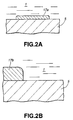
- the edges of the end portions of the counter electrodes can be rounded because of the fluidity and the surface tension of the material as shown in FIG. 2A which is a partially-enlarged view showing the counter electrode 17b and FIG. 2B which is an enlarged view of the foregoing portion of the counter electrode 17b.
- FIG. 2A which is a partially-enlarged view showing the counter electrode 17b
- FIG. 2B which is an enlarged view of the foregoing portion of the counter electrode 17b.
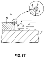
- the counter electrodes 17a and 17b substantially free from edges can be formed. Therefore, the concentration of electric fields as described with reference to FIG. 17 can be relaxed. As a result, formation of relatively large particles of silver deposited from the silver-salt solution 1 can be prevented.
- the first embodiment is able to prevent formation of inactive silver particles on the counter electrodes 17a and 17b which float in the silver-salt solution 1 and which deteriorate the transparency of the device when decoloring of the working electrode is performed and which cause the electrodes to be short-circuited.
- the silver-salt solution 1 may be solution prepared by dissolving silver halide, such as silver bromide, silver chloride or silver iodide in water or nonaqueous solvent.
- the nonaqueous solvent may be dimethylsulfoxide (DMSO), dimethylformamide (DMF), diethylformamide (DEF), N, N-dimethylacetoamide (DMAA), N-methylpropionate amide (MPA), N-methylpyrolidone (MP), propylenecarbonate (PC), acetonitril (AN), 2-methoxyethanol (MEOH), 2-ethoxyethanol (EEOH) or the like.
- the concentration of the silver halide in the silver-salt solution is 0.03 mol/l to 2.0 mol/l, preferably 0.05 mol/l to 2.0 mol/l.
- support salt capable of supplying halogen, such as bromine and so forth, is added.
- halogen such as bromine and so forth
- sodium halide, potassium halide, calcium halide, halogenated quaternary ammonium salt or the like may be employed.
- the supporting salt is added in a density ratio from 1/2 time to 5 times.
- the chemical modification is surface treatment (chemical plating) of the ITO electrode which is performed with palladium obtained by a two-part processing method of tin solution and palladium solution. That is, when palladium cores are deposited on the sole ITO substrate as a process for activating the surface of the ITO electrode with palladium, the activity on the surface of the ITO electrode can be improved.
- the tin solution may be solution prepared by dissolving 0.10 g to 1.0 g tin chloride (SnCl 2 ) in 1 liter HCl at a concentration of 0.010 % to 0.10 %.
- the palladium solution may be solution prepared by dissolving 0.10 g to 1.0 g palladium chloride (PdCl 2 ) in 1 liter HCl at a concentration of 0.010 % to 0.10 %.
- the physical modification method may be a method with which metal or the like which is more noble than silver is evaporated on the ITO electrode.
- FIGS. 1 and 2 A second embodiment of the present invention will now be described. Since the structure of the device according to the second embodiment is substantially the same as that according to the first embodiment shown in FIGS. 1 and 2, also the second embodiment will now be described with reference to FIGS. 1 and 2.
- the second embodiment has an arrangement that the counter electrodes 17a and 17b are formed by sintering the conductive particles.
- the other structures are the same as those according to the first embodiment.
- the conductive particles may be metal, such as silver or other metal or an alloy or a carbon material, such as graphite, soft carbon, hard carbon, carbon black, active carbon or their mixture. It is preferable that the particle size of the conductive particles is several mm to tens of mm. If the particle size is smaller than the above-mentioned range, the quantity of the conductive particle is relatively enlarged with respect to a required thickness of the film. Thus, there is apprehension that the cost cannot be reduced. If the particle size is larger than the above-mentioned range, vacancies in the film obtained by sintering are enlarged excessively. In this case, the mechanical strength of the film is reduced or the electric resistance is excessively raised.
- binder may be mixed before the mixing process is performed.
- the binder may be the binder according to the first embodiment.
- the second embodiment has the structure that the counter electrodes 17a and 17b are formed by sintering the conductive particles, such as metal or the carbon material after they have been previously molded. Then, the counter electrodes 17a and 17b are secured to the substrate by bonding or the like. Therefore, the quantity of the material can be reduced as compared with a structure that the counter electrodes are formed by closed-packed metal plates or the like. As a result, the cost of the material of the counter electrodes 17a and 17b can be reduced.
- each of the counter electrodes 17a and 17b which can be obtained by sintering powder can be obtained by forming a predetermined powder layer by a previous molding process which is performed before the sintering process. Then, the power layer is sintered so that the foregoing shape is obtained. Therefore, a shape similar to that of the powder layer can be obtained.
- counter electrodes 17a and 17b substantially free from edges can be formed, for example, as shown in FIGS. 2A and 2B. Therefore, the concentration of electric fields as described with reference to FIG. 17 can be relaxed. As a result, formation of relatively large particles of silver deposited from the silver-salt solution 1 can be prevented.
- the second embodiment is able to prevent formation of inactive silver particles on the counter electrodes 17a and 17b which float in the silver-salt solution 1 and which deteriorate the transparency of the device when decoloring of the working electrode is performed and which cause the electrodes to be short-circuited.
- the third embodiment has a structure that a lower conductive layer 18 in the form of metal foil made of silver, copper, stainless steel or ITO is provided for each of substrates 4 and 5 (the substrate 5 is illustrated) with a bonding agent or the like.
- a paste layer 19 is formed on the lower conductive layer 18.
- the lower conductive layer 18 and the paste layer 19 form counter electrodes 17a and 17b (the counter electrode 17b is illustrated) substantially similar to those shown in FIG. 1.
- the paste layer 19 has the composition similar to that of the counter electrodes 17a and 17b according to the first embodiment. That is, the paste layer 19 is formed by conductive paste prepared by mixing conductive particles composed of a metal material, such as silver, and carbon material, and a binder. The type, the mixture ratio and the like of the conductive particles and the binder may substantially the same as those according to the first embodiment.
- the other structures of the third embodiment are the same as those of the first embodiment. Therefore, the same structures are omitted from description.
- the third embodiment has the structure that the surface layers of the counter electrodes 17a and 17b are made of the mixture of the conductive particles and the binder, the cost of the material of the counter electrodes 17a and 17b can be reduced as compared with the structure in which the overall bodies of the counter electrodes are made of metal plates or the like.
- the paste layer 19 which is the surface layer of each of the counter electrodes 17a and 17b has substantially no edges as described in the first embodiment with reference to FIG. 2. Therefore, also the third embodiment is able to form the counter electrodes 17a and 17b which is substantially free from edges. Thus, the concentration of electric fields as described with reference to FIG. 17 can be relaxed. As a result, formation of relatively large particles of silver deposited from the silver-salt solution 1 can be prevented. Thus, also the third embodiment is able to prevent formation of inactive silver particles on the counter electrodes 17a and 17b which float in the silver-salt solution 1 and which deteriorate the transparency of the device when decoloring of the working electrode is performed and which cause the electrodes to be short-circuited.
- the third embodiment has the structure that the lower conductive layer 18 having relatively great mechanical strength and low resistance is formed below the paste layer 19. Therefore, the overall mechanical strength of each of the counter electrodes 17a and 17b can be raised and the electric resistance of the same can be lowered. Since the electric resistance of each of the counter electrodes 17a and 17b can be lowered as described above, the optical apparatus can be operated with a low voltage.
- the third embodiment may be structured such that the lower conductive layer 18 is made of ITO which is the same material as that for making the working electrode.
- the lower conductive layer 18 can conveniently be formed in the same process for forming the working electrodes 2a to 2e and 3a to 3e (see FIG. 1).
- the structure of the third embodiment may be combined with the structure of the second embodiment. That is, surface layers of the counter electrodes 17a and 17b may be formed by sintered layers formed by sintering the conductive particles in place of the paste layer 19. Also in the foregoing case, an effect substantially similar to that obtainable from the foregoing structures can be obtained.
- FIG. 4 a fourth embodiment of the present invention will now be described. As shown in FIG. 4, the structure of the fourth embodiment is formed by applying the present invention to the electrochemical dimming device described with reference to FIGS. 13 and 14.
- a pair of transparent substrates (for example, glass substrates) 24 and 25 serving as display windows are disposed apart from each other for a predetermined distance.
- Working electrodes (for example, ITO electrodes) 22 and 23 are formed on the inner surfaces (opposite surfaces) of the substrates 24 and 25.
- Silver-salt solution 21 is placed between the opposite working electrodes 22 and 23.
- a spacer 28 in the form of, for example, a glass plate or the like is disposed between the outer peripheries of the outer peripheries of the substrates 24 and 25.
- a counter electrode 27 formed by conductive paste similar to that according to the first embodiment or a sintered layer similar to the second embodiment is formed on the inner surface of the spacer 28 (see FIG. 4).
- the fourth embodiment has the structure that the counter electrode 27 is formed on only the surface of the spacer 28, the cost of the material of the spacer can considerably be reduced as compared with the conventional structure arranged such that the overall body of the spacer serving as the counter electrode is formed by a silver plate or the like.
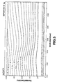
- FIGS. 5 to 10 show results of experiments of the relationship between the wavelength of light and transmittance of the ITO working electrode when the conductive paste and the sintered carbon layer are used as the counter electrodes according to the fourth embodiment.
- the axis of ordinate stands for the transmittance [%]
- axis of abscissa stands for the wavelength [nm] of light.
- silver salt silver bromide was employed, and DMSO was employed as the solvent.
- concentration of AgBr was made to be 500 mM/l.
- the supporting salt 500 mM/l tetra-n-butyl ammonia iodide was dissolved so that electrolyte was prepared.
- an ITO transparent electrode having a diameter of 7 mmf was employed.
- FIGS. 5 and 6 show change in the transmittance when silver was deposited on the working electrode and that when silver was dissolved from the working electrode in a case where conductive paste prepared such that the mixture ratio (the weight ratio) of the binder (an epoxy type binder) and silver particles was about 90:10 was employed as the counter electrode.
- the operation was performed by a constant potential method. When silver was deposited as shown in FIG. 5, the operation was performed at an applied voltage level of - 0.8 V for two seconds. When silver was dissolved as shown in FIG. 6, the operation was performed at an applied voltage level of +1.0 V for two seconds.
- FIGS. 7 and 8 show change in the transmittance when silver was deposited on the working electrode and that when silver was dissolved from the working electrode in a case where conductive paste prepared such that the mixture ratio (the weight ratio) of the binder (an epoxy type binder) and carbon black particles was about 80:20 was employed as the counter electrode.
- the operation was performed by a constant potential method. When silver was deposited as shown in FIG. 7, the operation was performed at an applied voltage level of - 0.8 V for two seconds. When silver was dissolved as shown in FIG. 8, the operation was performed at an applied voltage level of +1.0 V for two seconds.
- the decoloring (dissolution of silver as shown in FIG. 8) speed is somewhat reduced as compared with the structure in which the silver paste is employed as shown in FIGS. 5 and 6.
- coloring (silver deposition shown in FIG. 7) speed of the working electrode can be raised (therefore, the operation speed of the device is raised).
- FIGS. 9 and 10 show change in the transmittance when silver was deposited on the working electrode and that when silver was dissolved from the working electrode in a case where the sintered carbon layer was employed as the counter electrode.
- the operation was performed by a constant potential method. When silver was deposited as shown in FIG. 9, the operation was performed at an applied voltage level of - 1.2 V for two seconds. When silver was dissolved as shown in FIG. 10, the operation was performed at an applied voltage level of +0.5 V for two seconds.
- the following table shows a state of generation of deposits on the counter electrode when the silver plate (conventional example), the silver paste, the carbon paste and the sintered carbon layer were employed as the counter electrode in the experiments described with reference to FIGS. 5 to 10 after the optical apparatus was operated 20,000 times.
- the present invention using the conductive paste or the sintered layer is able to prevent formation of inactive silver particles on the counter electrode.
- contamination of the silver-salt solution because of the inactive silver particles can be prevented.
- FIGS. 11 and 12 a fifth embodiment of the present invention will now be described.
- the fifth embodiment has a structure that the present invention is applied to an electrochemical dimming device similar to that according to the fourth embodiment. Since the structures except for the material of the counter electrode 27 are the same, common elements are omitted from description.
- the counter electrodes are formed by applying or printing paste prepared by mixing carbon serving as the conductive particles with a variety of binders at a variety of mixing ratios and by applying or printing a material obtained by adding silver particles to the foregoing mixture (paste) in a predetermined quantity.
- the binder and the conductive particles are selected from those according to the first embodiment.
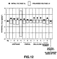
- the counter electrodes formed by changing the type of the binder and the mixing ratio of carbon and by adding the silver particles were used to measure the potential (initial potential V 0 : Vvs.Ag/Ag + ) between electrodes immediately after the electrodes were immersed in electrolyte.
- an ITO electrode was employed and operation was performed as shown in FIG. 11A such that the sweeping speed was 100 mV/S from a voltage level of - 0.75 V on the reduction side to that of +1.5 V on the oxidizing side.
- the degree of polarization (polarized voltage) of each electrode indicated with DV shown in FIG. 11B was measured and evaluated. Results are shown in the following Table 1 and FIG. 12.
- Figures provided for each binder shown in Table 1 and FIG. 12 are mixture ratios of carbon with respect to the various binders (for example, Urethane 1 indicates a weight ratio between urethane resin:carbon which is 99:1).
- the initial voltage V 0 is moved in a positive direction by 50 mV or greater as compared with silver. Even if the composition ratio is varied, it is difficult to design the initial value V 0 to be a similar level to the potential of silver. Moreover, also the polarized voltage DV is raised.
- the foregoing natural rubber has an average molecular with of 50,000 to 60,000, specifically, 55,000.
- another binder containing carboxymethyl cellulose (having an average molecular weight of 20,000 to 30,000, specifically, 22,000) may be employed to obtain a similar effect.
- the optical apparatus When the optical apparatus is operated by using the counter electrode to which no silver is added, silver is deposited on the counter electrode. Therefore, the composition of the counter electrode is changed as time elapses and thus the potential can easily be shifted. When silver is previously added as described above, the device can stably be operated.
- the device comprising the counter electrode formed by natural rubber 2 + silver powder by 10 % added is free from a large amount of deposits on the counter electrode.
- data of transmittance similar to that shown in FIGS. 5 and 6 can be obtained.
- the counter electrode is fully formed by the application or the like according to the present invention. At least the surface of the counter electrode adjacent to the silver-salt solution may be formed by the application or the like according to the present invention (in the foregoing case, the ground may be made of usual metal as employed in the third embodiment).
- the pattern of the electrode shown in FIG. 1 is not limited to the concentric shape. The pattern may be changed to any one of a stripe pattern, a lattice pattern and so forth. A cell may be provided for each of the divided electrodes.
- optical apparatus may be combined with another known filter member (for example, an organic electrochromic member, liquid crystal, an electroluminescent material).
- another known filter member for example, an organic electrochromic member, liquid crystal, an electroluminescent material.
- the optical apparatus according to the present invention can variously be applied as an apparatus for adjusting the liquid quantity of any one of various optical systems, for example, electrophotographic copying machine, an optical communication apparatuses and so forth as well as the optical diaphragm of the CCD.
- the optical apparatus according to the present invention may be applied to any one of various image display units for displaying characters and images as well as the optical filter.
- the present invention has the structure that at least the surface of either of the electrodes of an optical device, such as an electrochemical dimming device, using deposition/dissolution of silver is formed by the mixture of the conductive particles and the binder or the material obtained by sintering the conductive particles. Therefore, the cost of the material of the electrodes can be reduced as compared with the structure in which the overall body of the electrodes are made of metal plates or the like.
- either of the electrodes can be made to be substantially free from edges, local concentration of electric fields on the electrode can be relaxed. As a result, deposition of inactive and granular silver on the electrode can be reduced or prevented. As a result, floating of the inactive silver particles in the silver-salt solution which causes the transparency of the device to deteriorate and shortcut to take between the electrodes can be prevented.
Landscapes
- Physics & Mathematics (AREA)
- Nonlinear Science (AREA)
- General Physics & Mathematics (AREA)
- Engineering & Computer Science (AREA)
- Optics & Photonics (AREA)
- Computer Hardware Design (AREA)
- Theoretical Computer Science (AREA)
- Chemical & Material Sciences (AREA)
- Inorganic Chemistry (AREA)
- Electrochromic Elements, Electrophoresis, Or Variable Reflection Or Absorption Elements (AREA)
Applications Claiming Priority (5)
| Application Number | Priority Date | Filing Date | Title |
|---|---|---|---|
| JP1847197 | 1997-01-31 | ||
| JP18471/97 | 1997-01-31 | ||
| JP10009458A JPH10274790A (ja) | 1997-01-31 | 1998-01-21 | 光学装置及びその製造方法 |
| JP9458/98 | 1998-01-21 | ||
| PCT/JP1998/000410 WO1998034153A1 (fr) | 1997-01-31 | 1998-01-30 | Dispositif optique et procede de fabrication |
Publications (2)
| Publication Number | Publication Date |
|---|---|
| EP0897128A1 true EP0897128A1 (de) | 1999-02-17 |
| EP0897128A4 EP0897128A4 (de) | 2000-09-27 |
Family
ID=26344195
Family Applications (1)
| Application Number | Title | Priority Date | Filing Date |
|---|---|---|---|
| EP98901077A Withdrawn EP0897128A4 (de) | 1997-01-31 | 1998-01-30 | Optische vorrichtung und deren herstellungsverfahren |
Country Status (5)
| Country | Link |
|---|---|
| US (1) | US6219173B1 (de) |
| EP (1) | EP0897128A4 (de) |
| JP (1) | JPH10274790A (de) |
| KR (1) | KR20000064815A (de) |
| WO (1) | WO1998034153A1 (de) |
Cited By (1)
| Publication number | Priority date | Publication date | Assignee | Title |
|---|---|---|---|---|
| US6330099B1 (en) | 2000-03-24 | 2001-12-11 | Agilent Technologies, Inc. | Liquid crystal apron and skirt isolation for silicon micro displays |
Families Citing this family (13)
| Publication number | Priority date | Publication date | Assignee | Title |
|---|---|---|---|---|
| US6631022B1 (en) * | 1999-05-28 | 2003-10-07 | Sony Corporation | Optical device, a fabrication method thereof, a driving method thereof and a camera system |
| ATE415644T1 (de) * | 2000-05-04 | 2008-12-15 | Schott Donnelly Llc | Verfahren zur herstellung einer electrochromen tafel |
| US6373618B1 (en) * | 2000-05-04 | 2002-04-16 | Schott-Donnelly, Llc | Chromogenic glazing for automobiles and display filters |
| KR100697372B1 (ko) * | 2000-12-20 | 2007-03-20 | 비오이 하이디스 테크놀로지 주식회사 | 리튬이차 박막전지를 이용한 반사형 액정 디스플레이제조방법 |
| JP4569176B2 (ja) * | 2004-06-03 | 2010-10-27 | コニカミノルタホールディングス株式会社 | 表示素子 |
| WO2006087815A1 (ja) * | 2005-02-21 | 2006-08-24 | Fujitsu Limited | エレクトロデポジション表示装置およびその製造方法 |
| WO2007032117A1 (ja) * | 2005-09-14 | 2007-03-22 | Konica Minolta Holdings, Inc. | 表示素子の駆動方法 |
| JP2007328278A (ja) * | 2006-06-09 | 2007-12-20 | Fuji Xerox Co Ltd | 表示方法、表示媒体、及び表示素子 |
| JP2008180998A (ja) * | 2007-01-25 | 2008-08-07 | Sony Corp | エレクトロクロミック装置 |
| JP5740889B2 (ja) * | 2010-09-28 | 2015-07-01 | 凸版印刷株式会社 | 固体高分子形燃料電池用の炭素被覆触媒物質、その製造方法、電極触媒層、及び膜電極接合体 |
| JP2012128457A (ja) * | 2012-03-23 | 2012-07-05 | Stanley Electric Co Ltd | カメラ用絞り光学素子及びその製造方法 |
| US10895794B2 (en) * | 2013-09-10 | 2021-01-19 | Nanyang Technological University | Electrochromic device having a patterned electrode free of indium tin oxide (ITO) |
| US10663819B2 (en) * | 2018-08-07 | 2020-05-26 | Shenzhen China Star Optoelectronics Technology Co., Ltd. | Opposite substrate and preparation method thereof, and display device |
Family Cites Families (12)
| Publication number | Priority date | Publication date | Assignee | Title |
|---|---|---|---|---|
| US4365634A (en) * | 1979-12-06 | 1982-12-28 | C. R. Bard, Inc. | Medical electrode construction |
| JPS6315230A (ja) * | 1986-07-08 | 1988-01-22 | Hitachi Maxell Ltd | エレクトロクロミツク表示素子 |
| JPH04233210A (ja) * | 1990-12-28 | 1992-08-21 | Murata Mfg Co Ltd | 電気二重層コンデンサ |
| JP3428603B2 (ja) | 1995-03-20 | 2003-07-22 | ソニー株式会社 | 光学装置及び電解液 |
| JP3433411B2 (ja) | 1994-11-11 | 2003-08-04 | ソニー株式会社 | 光学装置 |
| US5764401A (en) * | 1994-11-11 | 1998-06-09 | Sony Corporation | Optical apparatus |
| US5840432A (en) * | 1995-02-13 | 1998-11-24 | Hitachi Chemical Company, Ltd. | Electroconductive paste |
| HUP9900853A2 (hu) * | 1995-06-07 | 1999-07-28 | Monsanto Co. | Eszköz és eljárás fény modulálására |
| US6019955A (en) * | 1996-03-08 | 2000-02-01 | Energy Conversion Devices, Inc. | Active nickel hydroxide material having controlled water content |
| US5864420A (en) * | 1996-03-08 | 1999-01-26 | Sony Corporation | Optical unit and electrolytic solution |
| JP3904101B2 (ja) * | 1996-09-20 | 2007-04-11 | ソニー株式会社 | 光学装置及び電解液 |
| WO1998014825A1 (en) * | 1996-10-01 | 1998-04-09 | National Label Company | Apparatus and method for assembling electrochromic cells |
-
1998
- 1998-01-21 JP JP10009458A patent/JPH10274790A/ja active Pending
- 1998-01-30 KR KR1019980707781A patent/KR20000064815A/ko not_active Abandoned
- 1998-01-30 EP EP98901077A patent/EP0897128A4/de not_active Withdrawn
- 1998-01-30 WO PCT/JP1998/000410 patent/WO1998034153A1/ja not_active Ceased
- 1998-01-30 US US09/155,472 patent/US6219173B1/en not_active Expired - Fee Related
Cited By (1)
| Publication number | Priority date | Publication date | Assignee | Title |
|---|---|---|---|---|
| US6330099B1 (en) | 2000-03-24 | 2001-12-11 | Agilent Technologies, Inc. | Liquid crystal apron and skirt isolation for silicon micro displays |
Also Published As
| Publication number | Publication date |
|---|---|
| KR20000064815A (ko) | 2000-11-06 |
| WO1998034153A1 (fr) | 1998-08-06 |
| US6219173B1 (en) | 2001-04-17 |
| JPH10274790A (ja) | 1998-10-13 |
| EP0897128A4 (de) | 2000-09-27 |
Similar Documents
| Publication | Publication Date | Title |
|---|---|---|
| US6219173B1 (en) | Optical device and its manufacturing method | |
| US6631022B1 (en) | Optical device, a fabrication method thereof, a driving method thereof and a camera system | |
| Zhou et al. | Enhanced electrochromic performances and cycle stability of NiO-based thin films via Li–Ti co-doping prepared by sol–gel method | |
| EP1914781B1 (de) | Transparente Kohlenstoff-Nanoröhrchen-Elektrode mit leitfähigem Dispersionsmittel und Herstellungsverfahren dafür | |
| US5395678A (en) | Thin film color filter for liquid crystal display | |
| KR20040066784A (ko) | 표시 소자 | |
| US20050104136A1 (en) | Electrochromic device based on nanocrystalline materials | |
| Muto et al. | Polythiophene-based mesoporous counter electrodes for plastic dye-sensitized solar cells | |
| US6336753B1 (en) | Optical device, a fabricating method thereof, a driving method thereof and a camera system | |
| Tomšík et al. | Assembly and interaction of polyaniline chains: Impact on electro-and physical–chemical behavior | |
| JP2001051308A (ja) | 電気光学素子及びその製造方法、及び撮像装置 | |
| JP2010282128A (ja) | 表示媒体及び表示装置 | |
| JPH08262501A (ja) | 光学装置及び電解液 | |
| JP2001051307A (ja) | 光学装置、その製造方法、その駆動方法及びカメラシステム | |
| Yip et al. | Aqueous asymmetric pseudocapacitor featuring high areal energy and power using conjugated polyelectrolytes and Ti3C2T x MXene | |
| Kashyap et al. | Solid-state responses of electrochemically deposited polyaniline and polypyrrole-based symmetric supercapacitors in different pH conditions | |
| Kim et al. | Graphene electrode enabling electrochromic approaches for daylight-dimming applications | |
| Jeong et al. | Control of chirality and electrochromism in copolymer-type chiral PEDOT derivatives by means of electrochemical oxidation and reduction | |
| JPWO2009031422A1 (ja) | エレクトロクロミック表示素子の製造方法 | |
| JP3446839B2 (ja) | 光学フィルタ | |
| JP2001059979A (ja) | 光学装置及びその駆動方法、並びに撮像装置 | |
| JP4572426B2 (ja) | 光学装置及びその駆動方法並びに撮像装置 | |
| JP2001059980A (ja) | 光学装置及びその駆動方法、並びに撮像装置 | |
| Yeh et al. | Study on oxidation state dependent electrocatalytic ability for I−/I3− redox reaction of reduced graphene oxides | |
| US4508430A (en) | Electrochromic display cell I |
Legal Events
| Date | Code | Title | Description |
|---|---|---|---|
| PUAI | Public reference made under article 153(3) epc to a published international application that has entered the european phase |
Free format text: ORIGINAL CODE: 0009012 |
|
| 17P | Request for examination filed |
Effective date: 19980930 |
|
| AK | Designated contracting states |
Kind code of ref document: A1 Designated state(s): DE FR GB |
|
| A4 | Supplementary search report drawn up and despatched |
Effective date: 20000817 |
|
| AK | Designated contracting states |
Kind code of ref document: A4 Designated state(s): DE FR GB |
|
| RIC1 | Information provided on ipc code assigned before grant |
Free format text: 7G 02F 1/17 A, 7G 02F 1/15 B, 7G 02F 1/155 B |
|
| STAA | Information on the status of an ep patent application or granted ep patent |
Free format text: STATUS: THE APPLICATION HAS BEEN WITHDRAWN |
|
| 18W | Application withdrawn |
Effective date: 20060105 |