EP0897214A2 - Circuit d'interface large bande à bruit ultra-faible pour la lecture monophotonique de photodétecteur - Google Patents
Circuit d'interface large bande à bruit ultra-faible pour la lecture monophotonique de photodétecteur Download PDFInfo
- Publication number
- EP0897214A2 EP0897214A2 EP98112310A EP98112310A EP0897214A2 EP 0897214 A2 EP0897214 A2 EP 0897214A2 EP 98112310 A EP98112310 A EP 98112310A EP 98112310 A EP98112310 A EP 98112310A EP 0897214 A2 EP0897214 A2 EP 0897214A2
- Authority
- EP
- European Patent Office
- Prior art keywords
- fet
- gain
- load
- current
- gate
- Prior art date
- Legal status (The legal status is an assumption and is not a legal conclusion. Google has not performed a legal analysis and makes no representation as to the accuracy of the status listed.)
- Withdrawn
Links
Images


Classifications
-
- H—ELECTRICITY
- H03—ELECTRONIC CIRCUITRY
- H03F—AMPLIFIERS
- H03F3/00—Amplifiers with only discharge tubes or only semiconductor devices as amplifying elements
- H03F3/04—Amplifiers with only discharge tubes or only semiconductor devices as amplifying elements with semiconductor devices only
- H03F3/08—Amplifiers with only discharge tubes or only semiconductor devices as amplifying elements with semiconductor devices only controlled by light
- H03F3/082—Amplifiers with only discharge tubes or only semiconductor devices as amplifying elements with semiconductor devices only controlled by light with FET's
-
- H—ELECTRICITY
- H04—ELECTRIC COMMUNICATION TECHNIQUE
- H04N—PICTORIAL COMMUNICATION, e.g. TELEVISION
- H04N25/00—Circuitry of solid-state image sensors [SSIS]; Control thereof
- H04N25/70—SSIS architectures; Circuits associated therewith
- H04N25/76—Addressed sensors, e.g. MOS or CMOS sensors
- H04N25/77—Pixel circuitry, e.g. memories, A/D converters, pixel amplifiers, shared circuits or shared components
-
- H—ELECTRICITY
- H10—SEMICONDUCTOR DEVICES; ELECTRIC SOLID-STATE DEVICES NOT OTHERWISE PROVIDED FOR
- H10F—INORGANIC SEMICONDUCTOR DEVICES SENSITIVE TO INFRARED RADIATION, LIGHT, ELECTROMAGNETIC RADIATION OF SHORTER WAVELENGTH OR CORPUSCULAR RADIATION
- H10F39/00—Integrated devices, or assemblies of multiple devices, comprising at least one element covered by group H10F30/00, e.g. radiation detectors comprising photodiode arrays
- H10F39/80—Constructional details of image sensors
- H10F39/809—Constructional details of image sensors of hybrid image sensors
Definitions
- This invention relates to ultra-low noise photon detection in low light conditions and more specifically to an ultra-low noise, high gain interface circuit for single-photon readout of off-the-shelf photodetectors at video frame rates.
- Available photodetectors such as photodiodes and photoconductors are inexpensive, exhibit bandwidths that support current video frame rates, are sensitive to wavelengths well into the long IR band, and exhibit a high degree of pixel-to-pixel uniformity when used in an imaging array. However, these photodetectors have no gain, i.e. each incident photon generates a single electron, and thus photodetector imaging systems work very well in moderate to bright light conditions, but generate electrical signals at low light levels that are too small to be read-out by conventional readout circuits.
- the standard photodetector In low light conditions, the standard photodetector is replaced with an avalanche photodiode that exhibits enough gain so that conventional readout circuits can readout the data at video frame rates with a high signal-to-noise ratio (SNR).
- SNR signal-to-noise ratio
- the fabrication of avalanche photodiodes is much more difficult and expensive than standard photodetectors because they must exhibit very high controlled gain and very low noise.
- currently available avalanche photodiodes exhibit relatively poor uniformity, are constrained to much lower wavelengths than standard photodetectors (1.5 ⁇ m), and have limited sensitivity due to their relatively low quantum efficiency.
- Imaging intensified systems use an array of avalanche photodiodes to drive respective display elements such as CCDs or phosphors, and have even lower wavelength capabilities (approximately 0.6 ⁇ m max) due to the limitations of the photodiode.
- Chamberlain et al. "A Novel Wide Dynamic Range Silicon Photodetector and Linear Imaging Array" IEEE Transactions on Electron Devices, Vol. ED-31, No. 2, February 1984, pp. 175-182 describes a gate modulation technique for single-photon readout of standard photodetectors.
- Chamberlain provides a high gain current mirror that includes a load FET whose gate is connected to its drain to ensure subthreshold operation and to eliminate threshold voltage V T non-uniformity.
- the pixel-to-pixel V T non-uniformity associated with standard silicon CMOS fabrication processes would otherwise substantially degrade the performance of the imaging array.
- the signal from the photodetector is injected into the load FET thereby producing a signal voltage at the gate of a gain FET.
- This signal modulates the gain FET's gate voltage, thereby storing integrated charge in a storage capacitor that is readout and reset via a pair of FET switches.
- Chamberlain's particular gain modulation technique provides a large dynamic range and is capable of detecting wavelengths into the long IR range, the bandwidth of the current mirror severely restricts the bandwidth of the overall detector.
- the RC time constant seen by the photodetector is the parallel combination of the photodetector's capacitance and the resistance of the load FET. In subthreshold operation, the FET's transconductance is very low and, hence, its load resistance is very large, on the order of 10 14 ohms. As a result, the RC time constant is on the order of seconds.
- Chamberlain's gate modulation technique is only practically useful for imaging static scenes such as stars.
- the load FET is typically quite small. As a result, the load FET exhibits substantial 1/f noise, which under low light conditions seriously degrades the performance of the imaging array.
- Kozlowski et al. "SWIR staring FPA Performance at Room Temperature," SPIE Vol. 2746, pp. 93-100, April 1996 describes a phenomenon called “night glow” in the short wavelength infrared (SWIR) band that enables detection on very dark nights where photon flux is on the order of one hundred photons per imaging frame.
- Kozlowski details InGaAs and HgCdTe detector arrays for use with two different readout circuits. Both use Chamberlain's gate modulation technique but one also buffers the detector node to maintain constant detector bias. Unlike SWIR band and longer wavelength detector arrays, near IR and visible detectors are not sensitive to changes in detector bias, and thus buffering to maintain constant bias is irrelevant.
- the present invention provides an ultra-low noise, high gain interface circuit for single-photon readout of known photodetectors from the x-ray to long IR bands at video frame rates.
- the interface circuit is preferably fabricated using high quality epi or neutron transmutation doped wafers with a thin oxide to provide adequate threshold voltage V T uniformity.
- the present invention provides a high bandwidth, ultra low-noise interface circuit that is capable of single-photon readout of photodetectors in extremely low light conditions, i.e. photon flux levels approaching zero photons per sampling period.
- This circuit can be used to count incident photons on individual photodetectors or in an imaging array as the front-end to a conventional video system.
- One of the primary benefits of the current approach is that the circuit can use off-the-shelf photodetectors such as photodiodes or photoconductors that have zero gain rather than avalanche photodiodes.
- Known photodetectors are cheaper, more uniform, easier to fabricate, more reliable, less susceptible to noise and are available at much longer wavelengths than current avalanche photodiodes.
- a photodetector 10 injects a small-signal detector current I det into a load FET 12 causing its gate-to-source voltage to self-adjust. This in turn modulates the gate-to-source voltage of a gain FET 14 so that it conducts a signal current I sig that is an amplified facsimile of the photocurrent.
- the FETs which form a current mirror, are biased to provide a very large current gain. Current gains on the order of twelve million have been measured under laboratory conditions.
- a low noise, high gain amplifier 16 is connected in a negative feedback loop around the load FET's gate-to-source voltage to expand the circuit's bandwidth and reduce its noise figure.
- the interface circuit 17 defined by the current mirror and amplifier facilitates continuous or sampled readout of the signal current at very high bandwidths while maintaining a high SNR.
- the gain of amplifier 16 speeds up the self-adjustment of the load FET's gate-to-source voltage, effectively dividing the RC time constant seen by photodetector 10 by the gain.
- the amplifier's negative feedback loop appears to slow down towards the bandwidth set by the RC time constant thereby maintaining a stable gate voltage. It was unknown whether stability could be achieved at such low flux levels. Conventional wisdom would dictate that the amplifier would rail to either its supply voltage or ground thereby destroying the signal until the flux levels increased. As the flux increases, the amplifier recovers and speeds up to re-expand the circuit's bandwidth.
- the amplifier also pins the load FET's gate voltage for a given detector current so that its 1/f noise is transferred to the amplifier thereby lowering the circuit's noise figure such that single-photon sensitivity can be achieved.
- photodetector 10 is a photodiode whose anode 18 is held at a common voltage V common such as ground or +5V and whose cathode 20 injects photocurrent into the load FET's drain 22.
- the FET's source 24 is held at a bias voltage V bias , which can be generated off-chip or on-chip using bandgap reference circuits, that reverse biases photodiode 10.
- the photodiode also exhibits a parasitic capacitance C that is connected in parallel with the photodiode.
- InGaAs, HgCdTe, or III-V compound photodiodes that exhibit no gain can be employed in this configuration.
- the specific design will depend upon the desired operating temperature and wavelength and must provide a dark current that is much less than the illuminated detector current.
- the detector current I det is very small, load FET 12 operates in its subthreshold region, where the FET's channel is below the threshold for conduction, but some current flows anyway due to the small population of thermally energetic electrons.
- the load FET's transconductance g load which is the differential change in drain current induced by the modulation of the FET's gate-to-source voltage, is proportional to its drain current, i.e. the detector current I det .
- the FET transconductance is very small, which is necessary to achieve high current gain.
- the output resistance R seen by the photodiode is large, on the order of 10 14 ohms. Therefore, the photodiode's RC time constant, which is equal to the parallel combination of the parasitic capacitance C and the FET's output resistance R, is large, on the order of seconds.
- Amplifier 16 is connected in a negative feedback configuration around load FET 12's gate-to-source.
- the amplifier's input 25 is connected to the FET's source 24 and its output 26 is connected to the FET's gate 27.
- Amplifier 16 may be a single-ended inverting amplifier of the type shown in FIG. 5 or a differential amplifier of the type shown in FIG. 6. Single-ended amplifiers require less chip space but differential amplifiers provide higher gain and have better common mode rejection ratio (CMRR).
- CMRR common mode rejection ratio
- the amplifier, and specifically its negative feedback loop, speeds up the load FET's self-adjustment process by the gain of the amplifier.
- Typical amplifier gains are on the order of a million such that the effective time constant is on the order of microseconds, much less than the sampling intervals of contemporary digital video systems.
- the amplifier also stabilizes the voltage at gate 27 for a given flux such that it is insensitive to the load FET's 1/f noise.
- Gain FET 14 preferably shares a common gate 27 with load FET 12 to reduce V T non-uniformity.
- the gain FET's drain 28 is connected to the output terminal OUT and source 30 is connected to a gain voltage V gain , which can be generated off-chip or on-chip using bandgap reference circuits, that biases the gain FET to operate in saturation.
- the gain FET's transconductance g gain 2(k g I sig ) 1/2 .
- the gain FET's transconductance and, hence the interface circuit's current gain A I can be made relatively large by controlling the value of k g .
- the current gain A I is a function of the detector current I det . Specifically, the gain curve exhibits a logarithmic response.
- the interface circuit can be implemented with some or all P-channel FETs.
- the load FET's source is connected to the photodiode and its drain is connected to V bias .
- the amplifier establishes the reverse bias of the photodiode.
- the P-channel gain FET is connected the same as the N-channel gain FET.
- one of the FETs is N-channel and the other is P-channel.
- the interface circuit can be linearized so that the gain is independent of detector current by connecting large resistors in series with the respective FETs that dominate the FETs' transimpedances so that the current gain A I is set by the ratio of these resistors.
- FIG. 2 is an I-V plot (not to scale) illustrating the small-signal operation of the interface circuit shown in FIG. 1.
- the interface circuit operates in the reverse bias region of the photodiode's response curve 32, i.e. V ⁇ 0.
- the load FET's exponential load line 34 and the gain FET's quadratic load line 36 are plotted on opposite sides of the voltage axis for purposes of clarity.
- the slope of the load line represents the FET's transconductance.
- the photodiode's response curve 32 intersects the load FET's load line 34 thereby setting its gate-to-source voltage.
- the load FET's V gs maps to the gain FET's load line 36, which establishes the signal current I sig .
- a change in the incident flux causes the photodiode's response curve 32 to shift by ⁇ I det .
- the load FET's operating point moves along its load line 34 to the new point of intersection, i.e. the load FET self-adjusts its gate-to-source voltage by ⁇ V gs to conduct the photocurrent.
- the same ⁇ V gs moves the operating point of the gain FET along its load line 36 producing a change in signal current ⁇ I sig .
- the load FET is biased so that a small change in photocurrent induces a large change in gate-to-source voltage and gain FET is biased to that a small change in its gate-to-source voltage induces a large change in signal current.
- the load FET's load line 34 is relatively flat and the gain FET's load line 36 is relatively steep in the reverse biased region; much flatter and much steeper than actually shown in the I-V plot.
- the logarithmic nature of the current gain as a function of photocurrent is evident from the exponential and quadratic shapes of load lines 34 and 36.
- FIG. 3 is an alternate embodiment of the interface circuit in which the current gain is constant and the signal current I sig is sampled and readout at video frame rates.
- the interface circuit is "linearized" to remove the logarithmic dependence on photocurrent by connecting a pair of resistors R L and R G between the FETs' respective sources 24 and 30 and ground and connecting the gain FET's gate 38 at the top of the load resistor R L .
- the voltage at the gate of the load FET is pinned and its source voltage across the load resistor R L is modulated by the photocurrent.
- both resistors are implemented as switched capacitors whose resistance can be varied to set the current gain.
- the simplest switched capacitor includes a capacitor 40 and a FET switch 42 that are connected in parallel between the load/gain FET's source and ground.
- the FET switch 42 is pulse width modulated (PWM) to alternately charge and discharge the capacitor 40.
- PWM pulse width modulated
- the pulse width is controlled to set the resistance R L or R G of the switched capacitor to establish a desired current gain.
- the load lines 44 and 46 associated with the load and gain FETs, respectively are now linear with constant slopes (1/R L ) and (1/R G ) so that the current gain is held constant regardless of changes in photocurrent.
- the signal current I sig stores integrated charge in a storage capacitor 50 that is tied to supply voltage V S and readout and reset via a pair of FET switches 52 and 54.
- Access and reset FET switches 52 and 54 are connected between a terminal DISC and ground, respectively, and the common output terminal OUT.
- the gate 56 of access switch 52 is driven with a voltage V A that switches at a sampling frequency f s to sample the voltage V C developed across the storage capacitor and output a discrete voltage signal V sig at the DISC terminal.
- the gate 58 of reset switch 54 is driven with a voltage V R that switches at the same sampling frequency f s as the access switch but 180 degrees out of phase to discharge the storage capacitor 50.
- the sampling frequency f s exceeds the bandwidth defined by the RC time constant but is less than the circuit's expanded bandwidth so that the discrete voltage signal accurately tracks the small-signal detector current.
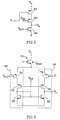
- FIG. 5 illustrates one embodiment of a single-ended amplifier for use in the interface circuits shown in FIGs. 1 and 3.
- an input signal V - whose voltage is more negative than was previously present causes the p-MOSFET driver 60 to conduct more strongly.
- the amplifier's output voltage subsequently swings to a more positive potential since the load FET's (an n-MOSFET device 62 whose nominal operating resistance is set by gate voltage V B1 ) relative operating resistance will be proportionally larger than before.
- An input signal V - whose voltage is more positive causes the driver MOSFET 60 to conduct less strongly; the resulting output voltage V o thus swings again in a direction opposite to that of the input signal.
- the open-loop gain of this basic cascoded CMOS inverter amplifier (with a p-MOSFET cascode 64 having identical geometry to the p-FET driver and biased by gate voltage V B2 ) is: where g m is the transconductance of the p-MOSFET amplifier, r d is the drain-source resistance of the load MOSFET and R L is the load resistance at the amplifier output. Since this load is often purely capacitive for the intended application, the denominator is often unity. In the absence of a cascode MOSFET, the gain is limited to -g m ⁇ r d .
- FIG. 6 illustrates one embodiment of a differential amplifier for use in the interface circuits shown in FIGs. 1 and 3.
- the input signal V - is applied to the inverting input leg 66 and a reference voltage V ref is applied to the non-inverting leg 68.
- the bias current I bias from the current source 70 is divided equally between both legs owing to the identical p-MOSFET drivers 72,74, p-MOS cascodes 76,78 having a common gate voltage V B3 and the Wilson load comprising an n-MOSFET current mirror with identical n-type transistors 80,82.
- an imaging array 90 is preferably fabricated with a hybrid structure.
- a photodetection layer 92 is grown using molecular beam epitaxy, for example, on a transparent detector substrate 94 to define an array of photodiodes 10.
- the interface circuit 17 for each photodiode is preferably fabricated in a silicon layer 96 using high quality epi or neutron transmutation doped wafers with a thin oxide to provide adequate threshold voltage V T uniformity.
- the photodetection layer 92 is flip-chip mounted on silicon layer 96 using an array of indium bumps 98 to connect the photodiodes 10 to respective interface circuits 17.
- a continuous illumination pattern 100 penetrates the detector substrate 94 where it is spatially sampled by the photodiode array.
- Each photodiode 10 generates a detector current that is proportional to the number of photons incident in that pixel area during each sampling interval.
- the detector currents I det are communicated through the indium bumps 98 to the respective interface circuits 17 where they are amplified and sampled.
- the discrete signals produced at each sampling instance together define one frame of a video signal, for example.
Landscapes
- Engineering & Computer Science (AREA)
- Power Engineering (AREA)
- Multimedia (AREA)
- Signal Processing (AREA)
- Amplifiers (AREA)
- Transforming Light Signals Into Electric Signals (AREA)
- Facsimile Scanning Arrangements (AREA)
- Measurement Of Radiation (AREA)
- Light Receiving Elements (AREA)
Applications Claiming Priority (3)
| Application Number | Priority Date | Filing Date | Title |
|---|---|---|---|
| US08/910,342 US5929434A (en) | 1997-08-13 | 1997-08-13 | Ultra-low noise high bandwidth interface circuit for single-photon readout of photodetectors |
| DE9100342 | 1997-08-13 | ||
| US910342 | 1997-08-13 |
Publications (2)
| Publication Number | Publication Date |
|---|---|
| EP0897214A2 true EP0897214A2 (fr) | 1999-02-17 |
| EP0897214A3 EP0897214A3 (fr) | 2000-07-19 |
Family
ID=25428647
Family Applications (1)
| Application Number | Title | Priority Date | Filing Date |
|---|---|---|---|
| EP98112310A Withdrawn EP0897214A3 (fr) | 1997-08-13 | 1998-07-02 | Circuit d'interface large bande à bruit ultra-faible pour la lecture monophotonique de photodétecteur |
Country Status (4)
| Country | Link |
|---|---|
| US (1) | US5929434A (fr) |
| EP (1) | EP0897214A3 (fr) |
| JP (1) | JPH11168670A (fr) |
| TW (1) | TW382182B (fr) |
Cited By (9)
| Publication number | Priority date | Publication date | Assignee | Title |
|---|---|---|---|---|
| EP1323193A2 (fr) * | 2000-09-25 | 2003-07-02 | Innovative Technology Licensing, LLC | Imageur ultraviolet haute performance pouvant etre utilise a temperature ambiante |
| GB2426575A (en) * | 2005-05-27 | 2006-11-29 | Sensl Technologies Ltd | Photon detector using controlled sequences of reset and discharge of a capacitor to sense photons |
| US7176439B2 (en) | 2003-07-09 | 2007-02-13 | National Institute Of Information And Communication Technology | Method for manufacturing photodetector for weak light |
| EP2160012A1 (fr) * | 2008-09-01 | 2010-03-03 | CSEM Centre Suisse d'Electronique et de Microtechnique SA - Recherche et Développement | Dispositif d'imagerie à photon unique |
| FR2950503A1 (fr) * | 2009-09-22 | 2011-03-25 | Soc Fr Detecteurs Infrarouges Sofradir | Circuit de detection avec derivation d'une partie du courant d'un photodetecteur et procede d'exploitation |
| CN102004003A (zh) * | 2010-09-27 | 2011-04-06 | 南通墨禾量子科技发展有限公司 | 光脉冲同步的高时间分辨率低噪声单光子探测器 |
| US8039782B2 (en) | 2003-09-19 | 2011-10-18 | Semiconductor Energy Laboratory Co., Ltd. | Optical sensor device and electronic apparatus with an amplifier circuit and dual level shift circuit |
| US9191586B2 (en) | 2013-07-08 | 2015-11-17 | Sensors Unlimited, Inc. | Buffered direct injection pixel for infrared detector arrays |
| US20230027347A1 (en) * | 2021-07-23 | 2023-01-26 | Nu-Trek, Inc. | Bias circuit with improved noise performance |
Families Citing this family (32)
| Publication number | Priority date | Publication date | Assignee | Title |
|---|---|---|---|---|
| US6147550A (en) * | 1998-01-23 | 2000-11-14 | National Semiconductor Corporation | Methods and apparatus for reliably determining subthreshold current densities in transconducting cells |
| JP2000078473A (ja) * | 1998-08-31 | 2000-03-14 | Canon Inc | 光電変換装置 |
| US6218905B1 (en) * | 1998-11-30 | 2001-04-17 | Vitesse Semiconductor | Common-gate transimpedance amplifier with dynamically controlled input impedance |
| US6809767B1 (en) * | 1999-03-16 | 2004-10-26 | Kozlowski Lester J | Low-noise CMOS active pixel sensor for imaging arrays with high speed global or row reset |
| US6844897B1 (en) * | 1999-06-15 | 2005-01-18 | Micron Technology, Inc. | Active pixel sensor (APS) readout structure with amplification |
| US6476374B1 (en) * | 2000-04-25 | 2002-11-05 | Innovative Technology Licensing, Llc | Room temperature, low-light-level visible imager |
| US6504141B1 (en) | 2000-09-29 | 2003-01-07 | Rockwell Science Center, Llc | Adaptive amplifier circuit with enhanced dynamic range |
| US6417504B1 (en) | 2000-09-29 | 2002-07-09 | Innovative Technology Licensing, Llc | Compact ultra-low noise high-bandwidth pixel amplifier for single-photon readout of photodetectors |
| US6965707B1 (en) | 2000-09-29 | 2005-11-15 | Rockwell Science Center, Llc | Compact active pixel with low-noise snapshot image formation |
| US6873359B1 (en) | 2000-09-29 | 2005-03-29 | Rockwell Science Center, Llc. | Self-adjusting, adaptive, minimal noise input amplifier circuit |
| US6900839B1 (en) * | 2000-09-29 | 2005-05-31 | Rockwell Science Center, Llc | High gain detector amplifier with enhanced dynamic range for single photon read-out of photodetectors |
| US6888572B1 (en) | 2000-10-26 | 2005-05-03 | Rockwell Science Center, Llc | Compact active pixel with low-noise image formation |
| US6538245B1 (en) * | 2000-10-26 | 2003-03-25 | Rockwell Science Center, Llc. | Amplified CMOS transducer for single photon read-out of photodetectors |
| US6919716B1 (en) * | 2002-08-28 | 2005-07-19 | Cisco Technology, Inc. | Precision avalanche photodiode current monitor |
| EP1475955B1 (fr) * | 2003-05-06 | 2006-05-31 | STMicroelectronics Limited | Système de calibration pour un capteur d'image logarithmique |
| US6937025B1 (en) * | 2003-07-17 | 2005-08-30 | Foveon, Inc. | Method and circuit employing current sensing to read a sensor |
| JP2005129909A (ja) * | 2003-09-19 | 2005-05-19 | Semiconductor Energy Lab Co Ltd | 光センサー装置および電子機器 |
| US20050068438A1 (en) * | 2003-09-30 | 2005-03-31 | Innovative Technology Licensing, Llc | Low noise CMOS amplifier for imaging sensors |
| US7046284B2 (en) * | 2003-09-30 | 2006-05-16 | Innovative Technology Licensing Llc | CMOS imaging system with low fixed pattern noise |
| JP4192880B2 (ja) * | 2004-10-12 | 2008-12-10 | セイコーエプソン株式会社 | 電気光学装置および電子機器 |
| US20070241377A1 (en) * | 2006-04-12 | 2007-10-18 | Semicoa | Back-illuminated photo-transistor arrays for computed tomography and other imaging applications |
| JP5143471B2 (ja) * | 2007-05-08 | 2013-02-13 | 株式会社日立製作所 | イメージング装置 |
| US7969476B1 (en) * | 2007-05-24 | 2011-06-28 | Advasense Technologies Ltd. | Method for accessing a pixel and a device having pixel access capabilities |
| JP5350912B2 (ja) * | 2009-04-13 | 2013-11-27 | セイコーインスツル株式会社 | 光検出回路及び電子機器 |
| US9209209B2 (en) * | 2010-10-29 | 2015-12-08 | Semiconductor Energy Laboratory Co., Ltd. | Photoelectric conversion device and method for operating the same |
| US8637800B2 (en) | 2011-04-19 | 2014-01-28 | Altasens, Inc. | Image sensor with hybrid heterostructure |
| CN103162842B (zh) * | 2013-04-02 | 2014-11-26 | 江苏物联网研究发展中心 | 具有自稳零电路的二极管红外探测器读出电路 |
| EP2797228B1 (fr) * | 2013-04-26 | 2016-04-20 | Xenics N.V. | Procédé pour détecter un courant photoélectrique |
| US9825189B2 (en) * | 2015-04-10 | 2017-11-21 | Sensors Unlimited, Inc. | Dual-mode photosensitive pixel with gain stage |
| KR101846017B1 (ko) * | 2017-09-18 | 2018-04-05 | 엘아이지넥스원 주식회사 | 노이즈 영상 생성 장치 및 방법 |
| CN112995472B (zh) * | 2021-02-07 | 2022-11-04 | 河北大学 | 基于零光子计数的单像素成像系统和成像方法 |
| EP4329193A1 (fr) * | 2022-08-25 | 2024-02-28 | NXP USA, Inc. | Circuit récepteur |
Family Cites Families (12)
| Publication number | Priority date | Publication date | Assignee | Title |
|---|---|---|---|---|
| US3770968A (en) * | 1972-02-24 | 1973-11-06 | Ibm | Field effect transistor detector amplifier cell and circuit for low level light signals |
| US3927383A (en) * | 1972-04-21 | 1975-12-16 | Rca Corp | Low noise wide band transducer system |
| US4473836A (en) * | 1982-05-03 | 1984-09-25 | Dalsa Inc. | Integrable large dynamic range photodetector element for linear and area integrated circuit imaging arrays |
| US4567363A (en) * | 1983-06-20 | 1986-01-28 | Santa Barbara Research Center | Switched capacitor transresistance amplifier |
| US4555623A (en) * | 1983-12-05 | 1985-11-26 | Irvine Sensors Corporation | Pre-amplifier in focal plane detector array |
| US4855687A (en) * | 1988-02-29 | 1989-08-08 | Micro Video, Inc | Transimpedance amplifier with noise reduction and bandwidth compensation |
| US5399989A (en) * | 1991-12-03 | 1995-03-21 | Rockwell International Corporation | Voltage amplifying source follower circuit |
| JPH05219443A (ja) * | 1992-02-05 | 1993-08-27 | Minolta Camera Co Ltd | 固体撮像装置 |
| US5473467A (en) * | 1994-07-08 | 1995-12-05 | At&T Corp. | Linear optical amplifier |
| US5589881A (en) * | 1994-11-09 | 1996-12-31 | The Regents Of The Univ. Of California Office Of Technology Transfer | Enhanced performance CCD output amplifier |
| US5572074A (en) * | 1995-06-06 | 1996-11-05 | Rockwell International Corporation | Compact photosensor circuit having automatic intensity range control |
| DE69533696D1 (de) * | 1995-08-31 | 2004-12-02 | St Microelectronics Srl | Strom-Generatorschaltung mit einem breiten Frequenzgang |
-
1997
- 1997-08-13 US US08/910,342 patent/US5929434A/en not_active Expired - Fee Related
-
1998
- 1998-07-02 EP EP98112310A patent/EP0897214A3/fr not_active Withdrawn
- 1998-08-04 JP JP10220151A patent/JPH11168670A/ja not_active Withdrawn
- 1998-10-31 TW TW087113285A patent/TW382182B/zh not_active IP Right Cessation
Cited By (14)
| Publication number | Priority date | Publication date | Assignee | Title |
|---|---|---|---|---|
| EP1323193A2 (fr) * | 2000-09-25 | 2003-07-02 | Innovative Technology Licensing, LLC | Imageur ultraviolet haute performance pouvant etre utilise a temperature ambiante |
| US7176439B2 (en) | 2003-07-09 | 2007-02-13 | National Institute Of Information And Communication Technology | Method for manufacturing photodetector for weak light |
| US8461509B2 (en) | 2003-09-19 | 2013-06-11 | Semiconductor Energy Laboratory Co., Ltd. | Optical sensor device including amplifier circuit and feedback resistor |
| US8039782B2 (en) | 2003-09-19 | 2011-10-18 | Semiconductor Energy Laboratory Co., Ltd. | Optical sensor device and electronic apparatus with an amplifier circuit and dual level shift circuit |
| US8017900B2 (en) | 2005-05-27 | 2011-09-13 | Sensl Technologies Ltd. | Photon counting apparatus |
| GB2426575A (en) * | 2005-05-27 | 2006-11-29 | Sensl Technologies Ltd | Photon detector using controlled sequences of reset and discharge of a capacitor to sense photons |
| EP2160012A1 (fr) * | 2008-09-01 | 2010-03-03 | CSEM Centre Suisse d'Electronique et de Microtechnique SA - Recherche et Développement | Dispositif d'imagerie à photon unique |
| FR2950503A1 (fr) * | 2009-09-22 | 2011-03-25 | Soc Fr Detecteurs Infrarouges Sofradir | Circuit de detection avec derivation d'une partie du courant d'un photodetecteur et procede d'exploitation |
| CN102004003A (zh) * | 2010-09-27 | 2011-04-06 | 南通墨禾量子科技发展有限公司 | 光脉冲同步的高时间分辨率低噪声单光子探测器 |
| CN102004003B (zh) * | 2010-09-27 | 2012-02-08 | 南通墨禾量子科技发展有限公司 | 光脉冲同步的高时间分辨率低噪声单光子探测器 |
| US9191586B2 (en) | 2013-07-08 | 2015-11-17 | Sensors Unlimited, Inc. | Buffered direct injection pixel for infrared detector arrays |
| BE1021861B1 (fr) * | 2013-07-08 | 2016-01-22 | Sensors Unlimited Inc. | Pixel a injection directe mis en memoire tampon pour matrices de detecteurs infrarouges |
| US20230027347A1 (en) * | 2021-07-23 | 2023-01-26 | Nu-Trek, Inc. | Bias circuit with improved noise performance |
| US11985442B2 (en) * | 2021-07-23 | 2024-05-14 | Nu-Trek, Inc. | Bias circuit with improved noise performance |
Also Published As
| Publication number | Publication date |
|---|---|
| US5929434A (en) | 1999-07-27 |
| TW382182B (en) | 2000-02-11 |
| JPH11168670A (ja) | 1999-06-22 |
| EP0897214A3 (fr) | 2000-07-19 |
Similar Documents
| Publication | Publication Date | Title |
|---|---|---|
| US5929434A (en) | Ultra-low noise high bandwidth interface circuit for single-photon readout of photodetectors | |
| Fossum et al. | Infrared readout electronics for space-science sensors: state of the art and future directions | |
| US6417504B1 (en) | Compact ultra-low noise high-bandwidth pixel amplifier for single-photon readout of photodetectors | |
| JP5014388B2 (ja) | 単一光子画像形成素子 | |
| US6384413B1 (en) | Focal plane infrared readout circuit | |
| US6323479B1 (en) | Sensor pixel with linear and logarithmic response | |
| US7746170B2 (en) | Class AB amplifier and imagers and systems using same | |
| JP2010063096A6 (ja) | 単一光子画像形成素子 | |
| US4857725A (en) | Differential offset corrected current mirror | |
| JPH08331457A (ja) | 光センサ回路 | |
| US6900839B1 (en) | High gain detector amplifier with enhanced dynamic range for single photon read-out of photodetectors | |
| US6538245B1 (en) | Amplified CMOS transducer for single photon read-out of photodetectors | |
| US10574913B2 (en) | High dynamic range CTIA pixel | |
| US8421016B2 (en) | Laser-pulse matrix detector with rapid summation | |
| EP0579751B1 (fr) | Amplificateur differentiel d'adaptation d'impedance | |
| Gasser et al. | Ultra sensitive PIN-diode receiver utilizing photocurrent integration on a parasitic capacitance | |
| JP3793033B2 (ja) | 赤外線センサ及びその駆動方法 | |
| US5220587A (en) | Output circuit for a CCD with a D.C. restoration circuit integrated together with the CCD in a monolithic semiconductor chip | |
| JPH0856011A (ja) | 受光素子、受光素子回路および受光素子アレイ | |
| US6768384B1 (en) | High-speed differential preamplifier | |
| US8981437B2 (en) | Wide bias background subtraction pixel front-end with short protection | |
| US6204496B1 (en) | Focal plane readout unit cell induced pulse diversion circuit and method | |
| Cunningham et al. | Noise and electrical characteristics below 10 K of small CHFET circuits and discrete devices | |
| US20040145667A1 (en) | Circuit arrangement, image-sensor device and method for reducing the smearing effect on an image sensor | |
| Pain | Focal plane infrared readout circuit |
Legal Events
| Date | Code | Title | Description |
|---|---|---|---|
| PUAI | Public reference made under article 153(3) epc to a published international application that has entered the european phase |
Free format text: ORIGINAL CODE: 0009012 |
|
| AK | Designated contracting states |
Kind code of ref document: A2 Designated state(s): GB |
|
| AX | Request for extension of the european patent |
Free format text: AL;LT;LV;MK;RO;SI |
|
| PUAL | Search report despatched |
Free format text: ORIGINAL CODE: 0009013 |
|
| AK | Designated contracting states |
Kind code of ref document: A3 Designated state(s): AT BE CH CY DE DK ES FI FR GB GR IE IT LI LU MC NL PT SE |
|
| AX | Request for extension of the european patent |
Free format text: AL;LT;LV;MK;RO;SI |
|
| RIC1 | Information provided on ipc code assigned before grant |
Free format text: 7H 03F 3/08 A, 7H 03F 3/345 B |
|
| 17P | Request for examination filed |
Effective date: 20000913 |
|
| AKX | Designation fees paid |
Free format text: GB |
|
| REG | Reference to a national code |
Ref country code: DE Ref legal event code: 8566 |
|
| STAA | Information on the status of an ep patent application or granted ep patent |
Free format text: STATUS: THE APPLICATION IS DEEMED TO BE WITHDRAWN |
|
| 18D | Application deemed to be withdrawn |
Effective date: 20040203 |