EP0898307A1 - Behandlungsverfahren zum Molekularkleben und Ablösen von zwei Strukturen - Google Patents
Behandlungsverfahren zum Molekularkleben und Ablösen von zwei Strukturen Download PDFInfo
- Publication number
- EP0898307A1 EP0898307A1 EP98402073A EP98402073A EP0898307A1 EP 0898307 A1 EP0898307 A1 EP 0898307A1 EP 98402073 A EP98402073 A EP 98402073A EP 98402073 A EP98402073 A EP 98402073A EP 0898307 A1 EP0898307 A1 EP 0898307A1
- Authority
- EP
- European Patent Office
- Prior art keywords
- structures
- bonding
- carried out
- interface
- heat treatment
- Prior art date
- Legal status (The legal status is an assumption and is not a legal conclusion. Google has not performed a legal analysis and makes no representation as to the accuracy of the status listed.)
- Granted
Links
Images


Classifications
-
- H—ELECTRICITY
- H10—SEMICONDUCTOR DEVICES; ELECTRIC SOLID-STATE DEVICES NOT OTHERWISE PROVIDED FOR
- H10P—GENERIC PROCESSES OR APPARATUS FOR THE MANUFACTURE OR TREATMENT OF DEVICES COVERED BY CLASS H10
- H10P90/00—Preparation of wafers not covered by a single main group of this subclass, e.g. wafer reinforcement
- H10P90/19—Preparing inhomogeneous wafers
- H10P90/1904—Preparing vertically inhomogeneous wafers
- H10P90/1906—Preparing SOI wafers
- H10P90/1914—Preparing SOI wafers using bonding
- H10P90/1916—Preparing SOI wafers using bonding with separation or delamination along an ion implanted layer, e.g. Smart-cut
-
- H—ELECTRICITY
- H10—SEMICONDUCTOR DEVICES; ELECTRIC SOLID-STATE DEVICES NOT OTHERWISE PROVIDED FOR
- H10P—GENERIC PROCESSES OR APPARATUS FOR THE MANUFACTURE OR TREATMENT OF DEVICES COVERED BY CLASS H10
- H10P72/00—Handling or holding of wafers, substrates or devices during manufacture or treatment thereof
- H10P72/70—Handling or holding of wafers, substrates or devices during manufacture or treatment thereof for supporting or gripping
- H10P72/74—Handling or holding of wafers, substrates or devices during manufacture or treatment thereof for supporting or gripping using temporarily an auxiliary support
-
- H—ELECTRICITY
- H10—SEMICONDUCTOR DEVICES; ELECTRIC SOLID-STATE DEVICES NOT OTHERWISE PROVIDED FOR
- H10W—GENERIC PACKAGES, INTERCONNECTIONS, CONNECTORS OR OTHER CONSTRUCTIONAL DETAILS OF DEVICES COVERED BY CLASS H10
- H10W10/00—Isolation regions in semiconductor bodies between components of integrated devices
- H10W10/10—Isolation regions comprising dielectric materials
- H10W10/181—Semiconductor-on-insulator [SOI] isolation regions, e.g. buried oxide regions of SOI wafers
-
- H—ELECTRICITY
- H10—SEMICONDUCTOR DEVICES; ELECTRIC SOLID-STATE DEVICES NOT OTHERWISE PROVIDED FOR
- H10P—GENERIC PROCESSES OR APPARATUS FOR THE MANUFACTURE OR TREATMENT OF DEVICES COVERED BY CLASS H10
- H10P72/00—Handling or holding of wafers, substrates or devices during manufacture or treatment thereof
- H10P72/70—Handling or holding of wafers, substrates or devices during manufacture or treatment thereof for supporting or gripping
- H10P72/74—Handling or holding of wafers, substrates or devices during manufacture or treatment thereof for supporting or gripping using temporarily an auxiliary support
- H10P72/743—Handling or holding of wafers, substrates or devices during manufacture or treatment thereof for supporting or gripping using temporarily an auxiliary support used as a support during manufacture of interconnect decals or build up layers
-
- Y—GENERAL TAGGING OF NEW TECHNOLOGICAL DEVELOPMENTS; GENERAL TAGGING OF CROSS-SECTIONAL TECHNOLOGIES SPANNING OVER SEVERAL SECTIONS OF THE IPC; TECHNICAL SUBJECTS COVERED BY FORMER USPC CROSS-REFERENCE ART COLLECTIONS [XRACs] AND DIGESTS
- Y10—TECHNICAL SUBJECTS COVERED BY FORMER USPC
- Y10S—TECHNICAL SUBJECTS COVERED BY FORMER USPC CROSS-REFERENCE ART COLLECTIONS [XRACs] AND DIGESTS
- Y10S148/00—Metal treatment
- Y10S148/012—Bonding, e.g. electrostatic for strain gauges
-
- Y—GENERAL TAGGING OF NEW TECHNOLOGICAL DEVELOPMENTS; GENERAL TAGGING OF CROSS-SECTIONAL TECHNOLOGIES SPANNING OVER SEVERAL SECTIONS OF THE IPC; TECHNICAL SUBJECTS COVERED BY FORMER USPC CROSS-REFERENCE ART COLLECTIONS [XRACs] AND DIGESTS
- Y10—TECHNICAL SUBJECTS COVERED BY FORMER USPC
- Y10S—TECHNICAL SUBJECTS COVERED BY FORMER USPC CROSS-REFERENCE ART COLLECTIONS [XRACs] AND DIGESTS
- Y10S148/00—Metal treatment
- Y10S148/135—Removal of substrate
Definitions
- the present invention relates to a method of treatment for bonding by molecular adhesion and takeoff of two structures.
- structure is meant any part of micromechanics, integrated optics, or microelectronics likely to be associated with a another piece by gluing.
- a structure can be, for example, a substrate or a support plate whether or not equipped with electronic, optical or mechanical.
- adhesion molecular is understood as a collage that highlights works an interaction between chemical terminations present on the surfaces of the structures contact.
- the invention finds applications in particular in the manufacture of integrated circuit devices. Indeed, in certain manufacturing processes, the semiconductor wafers containing circuits integrated must be secured with substrates stiffness, then separated at the end of treatment.
- the slices of semiconductor with electronic circuits integrated are in the form of plates thin and large.
- Standard manufacturing equipment microelectronics devices such as photorepeaters for example, are not suitable for treatment of such thin platelets.
- the thin semiconductor wafers exhibit a great fragility. This fragility is difficult compatible with handling steps, and including handling by automated processing.
- a thin wafer or surface layer a substrate with or without integrated circuits can be stuck on a processing medium again called "handle substrate".
- the handle substrate then provides sufficient mechanical strength to all the treatments and manipulations envisaged.
- FIG. 1 to 3 attached illustrate as an example a transfer of a layer thin including integrated circuits.
- the thin layer identified with the reference 10 in Figure 1, is initially attached to a substrate 12, called the original substrate. It includes components and integrated electronic circuits no represented.
- the original substrate 12 and the thin layer surface 10 are transferred onto a handle substrate 14 by sticking the thin surface layer on the handle substrate.
- the structure thus obtained is shown in Figure 1.
- the original substrate is then removed by a process such as rectification or cleavage, by chemical attack and / or polishing to obtain the structure of figure 2.
- the thin layer 10 comprising the circuits integrated, is now glued upside down on the handle substrate 14.
- the handle substrate thus provides to this layer the rigidity necessary for others manufacturing operations or processing.
- the thin layer 10 containing the circuits electronics is transferred to a target substrate or destination substrate 16 on which it is definitively fixed.
- the thin layer 10 is separated from the handle substrate 14. Also, the handle substrate 14 is shown in broken lines in Figure 3.
- the bonding of the thin layer 10 on the handle substrate 14 can be made, for example, to cold using an appropriate adhesive.
- the collage is then reversible and the separation of the thin layer 10 handle substrate is possible.
- membership obtained between the thin layer 10 and the handle substrate 14 may be insufficient, particularly for subsequent high temperature treatments.
- the glue is not able to support high temperatures.
- the material (glue) added for the sticking may cause contamination metallic or organic parts glued during subsequent treatments.
- a first step involves the preparation of surfaces of structures intended to be contact.
- Obtaining a molecular collage of quality requires control of important parameters such as surface roughness, which must be preferably less than 0.5 nm (5 ⁇ ), in value quadratic mean, the absence of dust (particles> 0.2 ⁇ m) on the surfaces, the flatness of surfaces to be contacted and the chemical state of these surfaces.
- the first step thus includes, for the essential, a cleaning of the surfaces of structures to stick in order to remove foreign particles and to make these surfaces hydrophilic.
- FIG. 4 shows a structure for bonding comprising a silicon substrate 20 of which a surface 22 has been made hydrophilic.
- the surface 22 has a first hydrophilic layer 24 consisting essentially of chemical groups Si-OH and one (or more) layer of water H 2 O 26 adsorbed on the hydrophilic layer 24.
- a second step involves contacting hydrophilic surfaces of the two structures to be bonded. This contacting allows to bring sufficiently close the layers of water adsorbed on the structures so that these interact. The attraction that is exercised between water molecules spreads close in close on the entire surface of each structure. The contact surfaces are then glued in their whole.
- the measurement of the bonding energy by a blade insertion method gives a value of the order of 0.15 J / m 2 .
- Such a value is typically that of a hydrogen type adhesion between the two layers of water, respectively of each structure.
- a third step involves treatment thermal adhesion solidification.
- the heat treatment allows, up to a temperature of the order of 200 ° C., removing the layers of water between the assembled structures.
- a possible fourth step includes heat treatment above 900 ° C. During this step, the interacting Si-OH groups evolve towards much stronger Si-O-Si bonds. We then observe a very strong increase in energy link.
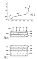
- the graph in FIG. 5 shows on the ordinate the bonding energy per unit area, between the structures bonded by molecular adhesion, as a function of the treatment temperature.
- the binding energies are expressed in J / m 2 and the temperatures in ° C.
- Regions 32, 33 and 34 of the curve of graph relate to second, third and fourth steps of the bonding process and correspond respectively to a hydrogen type interaction between water films, a hydrogen interaction between OH groups (reference 24) then a type interaction Si-O-Si.
- reference 24 a hydrogen interaction between OH groups
- Si-O-Si a type interaction between Si-O-Si.
- binding energies greater than 2 J / m 2 can be obtained. These energies are thus of the order of magnitude of the cohesion energies of the silicon material.
- the handle substrate is eliminated for example by running-in and / or by mechanical-chemical abrasion.
- the method of transferring a thin layer requires the sacrifice of a substrate handle for each thin layer treated. This sacrifice also represents a significant industrial cost.
- the object of the present invention is to provide a treatment for bonding two structures allowing, not only to obtain a collage very resistant molecular of the two structures but also allowing to take off the structures according to the bonding interface.
- An object of the invention is also to propose a treatment allowing a takeoff which does not damage assembled structures.
- the invention has more specifically for a processing method for the bonding of two structures by molecular adhesion according to a bonding interface, and takeoff of said two structures according to said interface of collage.
- thermal budget is meant, the sum of the heat treatments carried out and defined by a time / temperature pair applied to the structure.
- the heat treatment able to take off the two parts may take heat treatments into account before takeoff suffered by structures assemblies.
- a implantation of hydrogen in at least one of structures the hydrogen forming said element likely to diffuse in the structure.
- the implantation is carried out, for example, in silicon with a dose between 10 16 and 5.10 16 (H + / cm 2 ) and an energy between 20 and 500 KeV.
- the dose can be of the order of 3.10 16 ions / cm 2 and the implantation energy of the order of 70 KeV.
- the dose depends on the implantation conditions and in particular on the temperature of the structure during implantation.
- the heat treatment for takeoff can be carried out at a temperature between 600 and 1350 ° C. for example for silicon.
- this temperature is chosen rather of the order of 200 to 600 ° C.
- silicon carbide (S 1 C) the temperature is chosen from 600 ° C up to the melting temperature which is higher than 1350 ° C
- the heat treatment can take place, for example example, under heating lamps or in an oven.
- the structures to be assembled can be structures in one solid material but can also be multilayer structures containing areas that have been treated or not.
- the multilayer character of the structures can advantageously generate internal constraints which promote the separation of structures during the stage takeoff.
- FIG. 1 is a section schematic of a structure comprising a thin layer on a substrate, called the original substrate, assembled with another substrate, called handle substrate.
- FIG. 4 is a schematic section of a structure prepared for molecular bonding.
- FIG. 5 is a graph expressing the binding energy between two structures during stages of molecular bonding.
- FIG. 6 is a schematic section of a structure comprising a silicon wafer and illustrates the preparation of this structure for a molecular bonding according to the invention.
- Figure 7 shows in section the structure of Figure 6 pasted on another structure comprising a silicon wafer.
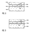
- FIG. 8 and 9 show in section the assembled structures of Figure 7, and illustrate a treatment stage for takeoff, in accordance with the invention.
- FIG. 10 shows in section another assembly obtained by molecular bonding of two structures according to the invention.
- FIG. 10 shows in section the assembly of FIG. 10 during a treatment for takeoff, according to the invention.
- FIG. 6 shows a structure 100 intended for molecular bonding in accordance with the invention.
- the structure 100 comprises a plate of silicon 102 covered with a layer of oxide of superficial silicon 104.
- An implanted hydrogen layer 106 is formed by implantation of hydrogen ions in the silicon plate 102 through the oxide layer 104.
- the hydrogen layer implanted at an energy of the order of 70 KeV, has , in this example, a concentration of 3.10 16 ions / cm 2 , a thickness of 400 nm and is buried at a depth of the order of 300 nm under the upper surface 110 of the structure 100. (The figures are not to scale and do not respect these proportions).
- hydrogen is meant the gaseous species constituted either in their atomic form (for example H) or in their molecular form (for example H 2 ) or in their ionic form (H + , H 2 + , ...) or in their isotopic (Deuterium) or isotopic and ionic form.
- the surface 110 of the structure 100 is then cleaned to make it hydrophilic and free of particles.
- a film of water (not shown in the figure) is formed on the surface 110.
- Low roughness can also be conferred or preserved on the surface 110 of the structure 100.
- the structure 100 is then assembled with a second structure 120.
- the second structure has a silicon wafer 122, whose surface in contact with the structure 100, also advantageously underwent cleaning for the make it hydrophilic.
- Reference 124 designates the interface between the structures 100 and 120 assembled.
- the structures then undergo a first annealing at a temperature of the order of 500 ° C. which allows to eliminate the layers of water between the structures assembled and which makes it possible to establish connections between the surfaces in contact.
- the bonding energy of the molecular bonding obtained at 500 ° C is of the order of 0.5 J / m 2 .
- Such a binding energy is sufficient, for example, to connect a silicon wafer containing integrated circuits to a handle substrate; it is in particular sufficient for all of the treatments envisaged for the wafer in the usual equipment for manufacturing microelectronic devices.
- the formation of the separation zones is controlled by the thermal budget applied to structures. Indeed, the heat treatment allows diffusing the hydrogen from the implanted layer 106 in the structure 100 towards the bonding interface 124. (Via oxide if present). The diffusing hydrogen is trapped at the interface 124, accumulates there and can evolve there under gaseous form. So the accumulation of hydrogen at the interface 124 makes it possible to counteract, at least in part, the bonding forces.
- diffusion of hydrogen towards interface 124 of collage is indicated by arrows 132.
- the detachment zones 130 can be local ( Figure 8) or extend over the entire interface surface (figure 9).
- the thermal budget necessary to obtain complete detachment depends on the quantity of the element liable to migrate present in the material of at least one of the structures.
- the thermal budget is therefore linked to the implantation dose of the hydrogen.
- the budget can be 900 ° C -30 min.
- Figure 10 shows another example of setting of the invention. It represents in section a assembly of a first structure 200 and a second structure 220 which are bonded by bonding molecular as previously described.
- the reference 224 designates the bonding interface between surfaces assembled structures.
- the first structure essentially comprises a silicon plate 202 on the surface of which formed a layer 206 of oxide.
- Layer oxide 206 is deposited by a channel deposition technique chemical vapor phase, plasma assisted (Plasma Enhanced Chemical Vapor Deposition). Such an oxide has peculiarity of containing OH molecules susceptible to broadcast.
- a first heat treatment, carried out at a temperature less than or equal to about 500 ° C allows to increase the energy of molecular bonding.
- the OH groups contained in the oxide layer 206 broadcast and migrate, notably to the interface 224 or they are trapped.
- the diffusion of OH groups towards the interface is indicated with arrows 232.
- the OH molecules evolve in gaseous form and are concentrated at the bonding interface. This phenomenon leads to bubble formation and induces embrittlement of the bonding interface.
- a detached area 230 is propagates until complete separation of the two structures 200 and 220.
- the separation of structures can be facilitated by the exercise of mechanical forces separation panels. These forces are represented by arrows 240, 241 in FIG. 11.
- the forces are 240 tensile forces and / or shear 241.
- the invention applies to any type of structure as defined above. It should be noted that the invention does not only relate to structures comprising silicon but also to other semiconductor structures (S i , S i C, A s G a ....), insulating structures (glass, quartz %) or even conductive structures (metal alloys ).
Landscapes
- Pressure Welding/Diffusion-Bonding (AREA)
- Element Separation (AREA)
- Formation Of Insulating Films (AREA)
- Recrystallisation Techniques (AREA)
Applications Claiming Priority (2)
| Application Number | Priority Date | Filing Date | Title |
|---|---|---|---|
| FR9710480 | 1997-08-19 | ||
| FR9710480A FR2767604B1 (fr) | 1997-08-19 | 1997-08-19 | Procede de traitement pour le collage moleculaire et le decollage de deux structures |
Publications (2)
| Publication Number | Publication Date |
|---|---|
| EP0898307A1 true EP0898307A1 (de) | 1999-02-24 |
| EP0898307B1 EP0898307B1 (de) | 2006-12-27 |
Family
ID=9510376
Family Applications (1)
| Application Number | Title | Priority Date | Filing Date |
|---|---|---|---|
| EP98402073A Expired - Lifetime EP0898307B1 (de) | 1997-08-19 | 1998-08-17 | Behandlungsverfahren zum Molekularkleben und Ablösen von zwei Strukturen |
Country Status (5)
| Country | Link |
|---|---|
| US (1) | US6429094B1 (de) |
| EP (1) | EP0898307B1 (de) |
| JP (1) | JP4316701B2 (de) |
| DE (1) | DE69836707T2 (de) |
| FR (1) | FR2767604B1 (de) |
Cited By (10)
| Publication number | Priority date | Publication date | Assignee | Title |
|---|---|---|---|---|
| US6566233B2 (en) | 1999-12-24 | 2003-05-20 | Shin-Etsu Handotai Co., Ltd. | Method for manufacturing bonded wafer |
| FR2835095A1 (fr) * | 2002-01-22 | 2003-07-25 | Soitec Silicon On Insulator | Procede de preparation d'ensembles a semi-conducteurs separables, notamment pour former des substrats pour l'electronique, l'optoelectrique et l'optique |
| FR2926672A1 (fr) * | 2008-01-21 | 2009-07-24 | Soitec Silicon On Insulator | Procede de fabrication de couches de materiau epitaxie |
| US7902038B2 (en) * | 2001-04-13 | 2011-03-08 | Commissariat A L'energie Atomique | Detachable substrate with controlled mechanical strength and method of producing same |
| US8048766B2 (en) | 2003-06-24 | 2011-11-01 | Commissariat A L'energie Atomique | Integrated circuit on high performance chip |
| US8252663B2 (en) | 2009-06-18 | 2012-08-28 | Commissariat A L'energie Atomique Et Aux Energies Alternatives | Method of transferring a thin layer onto a target substrate having a coefficient of thermal expansion different from that of the thin layer |
| US8309431B2 (en) | 2003-10-28 | 2012-11-13 | Commissariat A L'energie Atomique | Method for self-supported transfer of a fine layer by pulsation after implantation or co-implantation |
| US8389379B2 (en) | 2002-12-09 | 2013-03-05 | Commissariat A L'energie Atomique | Method for making a stressed structure designed to be dissociated |
| US8609514B2 (en) | 1997-12-10 | 2013-12-17 | Commissariat A L'energie Atomique | Process for the transfer of a thin film comprising an inclusion creation step |
| FR3029538A1 (fr) * | 2014-12-04 | 2016-06-10 | Soitec Silicon On Insulator | Procede de transfert de couche |
Families Citing this family (30)
| Publication number | Priority date | Publication date | Assignee | Title |
|---|---|---|---|---|
| FR2774511B1 (fr) * | 1998-01-30 | 2002-10-11 | Commissariat Energie Atomique | Substrat compliant en particulier pour un depot par hetero-epitaxie |
| FR2815121B1 (fr) * | 2000-10-06 | 2002-12-13 | Commissariat Energie Atomique | Procede de revelation de defauts cristallins et/ou de champs de contraintes a l'interface d'adhesion moleculaire de deux materiaux solides |
| JP2002270553A (ja) * | 2001-03-13 | 2002-09-20 | Mitsubishi Gas Chem Co Inc | 電子部品の製造法 |
| FR2823596B1 (fr) * | 2001-04-13 | 2004-08-20 | Commissariat Energie Atomique | Substrat ou structure demontable et procede de realisation |
| FR2837981B1 (fr) * | 2002-03-28 | 2005-01-07 | Commissariat Energie Atomique | Procede de manipulation de couches semiconductrices pour leur amincissement |
| JP4277481B2 (ja) * | 2002-05-08 | 2009-06-10 | 日本電気株式会社 | 半導体基板の製造方法、半導体装置の製造方法 |
| FR2856192B1 (fr) * | 2003-06-11 | 2005-07-29 | Soitec Silicon On Insulator | Procede de realisation de structure heterogene et structure obtenue par un tel procede |
| FR2857953B1 (fr) | 2003-07-21 | 2006-01-13 | Commissariat Energie Atomique | Structure empilee, et procede pour la fabriquer |
| FR2860178B1 (fr) * | 2003-09-30 | 2005-11-04 | Commissariat Energie Atomique | Procede de separation de plaques collees entre elles pour constituer une structure empilee. |
| JPWO2005045908A1 (ja) * | 2003-11-06 | 2007-05-24 | 松下電器産業株式会社 | 基板貼り合わせ方法、その貼り合わせ基板及び直接接合基板 |
| FR2880189B1 (fr) * | 2004-12-24 | 2007-03-30 | Tracit Technologies Sa | Procede de report d'un circuit sur un plan de masse |
| FR2889887B1 (fr) | 2005-08-16 | 2007-11-09 | Commissariat Energie Atomique | Procede de report d'une couche mince sur un support |
| JP4830418B2 (ja) * | 2005-09-16 | 2011-12-07 | 株式会社デンソー | 半導体装置 |
| FR2891281B1 (fr) | 2005-09-28 | 2007-12-28 | Commissariat Energie Atomique | Procede de fabrication d'un element en couches minces. |
| FR2903808B1 (fr) * | 2006-07-11 | 2008-11-28 | Soitec Silicon On Insulator | Procede de collage direct de deux substrats utilises en electronique, optique ou opto-electronique |
| US8124499B2 (en) * | 2006-11-06 | 2012-02-28 | Silicon Genesis Corporation | Method and structure for thick layer transfer using a linear accelerator |
| US20080128641A1 (en) * | 2006-11-08 | 2008-06-05 | Silicon Genesis Corporation | Apparatus and method for introducing particles using a radio frequency quadrupole linear accelerator for semiconductor materials |
| FR2910179B1 (fr) | 2006-12-19 | 2009-03-13 | Commissariat Energie Atomique | PROCEDE DE FABRICATION DE COUCHES MINCES DE GaN PAR IMPLANTATION ET RECYCLAGE D'UN SUBSTRAT DE DEPART |
| US20080188011A1 (en) * | 2007-01-26 | 2008-08-07 | Silicon Genesis Corporation | Apparatus and method of temperature conrol during cleaving processes of thick film materials |
| FR2925221B1 (fr) | 2007-12-17 | 2010-02-19 | Commissariat Energie Atomique | Procede de transfert d'une couche mince |
| FR2926674B1 (fr) | 2008-01-21 | 2010-03-26 | Soitec Silicon On Insulator | Procede de fabrication d'une structure composite avec couche d'oxyde de collage stable |
| FR2926748B1 (fr) * | 2008-01-25 | 2010-04-02 | Commissariat Energie Atomique | Objet muni d'un element graphique reporte sur un support et procede de realisation d'un tel objet. |
| FR2931014B1 (fr) * | 2008-05-06 | 2010-09-03 | Soitec Silicon On Insulator | Procede d'assemblage de plaques par adhesion moleculaire |
| FR2938117B1 (fr) * | 2008-10-31 | 2011-04-15 | Commissariat Energie Atomique | Procede d'elaboration d'un substrat hybride ayant une couche continue electriquement isolante enterree |
| US7927975B2 (en) | 2009-02-04 | 2011-04-19 | Micron Technology, Inc. | Semiconductor material manufacture |
| JP5524776B2 (ja) * | 2010-09-10 | 2014-06-18 | 日本電信電話株式会社 | 薄膜形成方法及びシートフィルム |
| US8524572B2 (en) * | 2011-10-06 | 2013-09-03 | Micron Technology, Inc. | Methods of processing units comprising crystalline materials, and methods of forming semiconductor-on-insulator constructions |
| US9481566B2 (en) | 2012-07-31 | 2016-11-01 | Soitec | Methods of forming semiconductor structures including MEMS devices and integrated circuits on opposing sides of substrates, and related structures and devices |
| FR3077924B1 (fr) * | 2018-02-13 | 2020-01-17 | Soitec | Structure demontable et procede de demontage utilisant ladite structure |
| FR3079532B1 (fr) | 2018-03-28 | 2022-03-25 | Soitec Silicon On Insulator | Procede de fabrication d'une couche monocristalline de materiau ain et substrat pour croissance par epitaxie d'une couche monocristalline de materiau ain |
Citations (3)
| Publication number | Priority date | Publication date | Assignee | Title |
|---|---|---|---|---|
| FR2501907A1 (fr) * | 1981-03-13 | 1982-09-17 | Thomson Csf | Procede de positionnement, de maintien d'un substrat plan sur une platine porte-substrat et de retrait de ce substrat ainsi que l'appareillage pour la mise en oeuvre du procede |
| WO1994017551A1 (en) * | 1993-01-19 | 1994-08-04 | Hughes Aircraft Company | Intermediate-temperature diffusion welding |
| EP0751556A1 (de) * | 1995-06-30 | 1997-01-02 | Commissariat A L'energie Atomique | Herstellungsverfahren eines Verdrahtungssubstrates zur Verbindung eines Chips zu einem Träger |
Family Cites Families (5)
| Publication number | Priority date | Publication date | Assignee | Title |
|---|---|---|---|---|
| US5503704A (en) * | 1993-01-06 | 1996-04-02 | The Regents Of The University Of California | Nitrogen based low temperature direct bonding |
| US5310451A (en) * | 1993-08-19 | 1994-05-10 | International Business Machines Corporation | Method of forming an ultra-uniform silicon-on-insulator layer |
| US5510277A (en) * | 1994-06-29 | 1996-04-23 | At&T Corp. | Surface treatment for silicon substrates |
| DE19648501A1 (de) * | 1996-11-22 | 1998-05-28 | Max Planck Gesellschaft | Verfahren für die lösbare Verbindung und anschließende Trennung reversibel gebondeter und polierter Scheiben sowie eine Waferstruktur und Wafer |
| US5882987A (en) * | 1997-08-26 | 1999-03-16 | International Business Machines Corporation | Smart-cut process for the production of thin semiconductor material films |
-
1997
- 1997-08-19 FR FR9710480A patent/FR2767604B1/fr not_active Expired - Lifetime
-
1998
- 1998-08-11 US US09/132,059 patent/US6429094B1/en not_active Expired - Lifetime
- 1998-08-17 EP EP98402073A patent/EP0898307B1/de not_active Expired - Lifetime
- 1998-08-17 DE DE69836707T patent/DE69836707T2/de not_active Expired - Lifetime
- 1998-08-19 JP JP23326898A patent/JP4316701B2/ja not_active Expired - Lifetime
Patent Citations (3)
| Publication number | Priority date | Publication date | Assignee | Title |
|---|---|---|---|---|
| FR2501907A1 (fr) * | 1981-03-13 | 1982-09-17 | Thomson Csf | Procede de positionnement, de maintien d'un substrat plan sur une platine porte-substrat et de retrait de ce substrat ainsi que l'appareillage pour la mise en oeuvre du procede |
| WO1994017551A1 (en) * | 1993-01-19 | 1994-08-04 | Hughes Aircraft Company | Intermediate-temperature diffusion welding |
| EP0751556A1 (de) * | 1995-06-30 | 1997-01-02 | Commissariat A L'energie Atomique | Herstellungsverfahren eines Verdrahtungssubstrates zur Verbindung eines Chips zu einem Träger |
Non-Patent Citations (1)
| Title |
|---|
| MASZARA W P ET AL: "BONDING OF SILICON WAFERS FOR SILICON-ON-INSULATOR", JOURNAL OF APPLIED PHYSICS, vol. 64, no. 10, PART 1, 15 November 1988 (1988-11-15), pages 4943 - 4950, XP000050002 * |
Cited By (19)
| Publication number | Priority date | Publication date | Assignee | Title |
|---|---|---|---|---|
| US8609514B2 (en) | 1997-12-10 | 2013-12-17 | Commissariat A L'energie Atomique | Process for the transfer of a thin film comprising an inclusion creation step |
| EP1187216A4 (de) * | 1999-12-24 | 2008-09-24 | Shinetsu Handotai Kk | Herstellungsmethode einer verbundscheibe |
| US6566233B2 (en) | 1999-12-24 | 2003-05-20 | Shin-Etsu Handotai Co., Ltd. | Method for manufacturing bonded wafer |
| US7902038B2 (en) * | 2001-04-13 | 2011-03-08 | Commissariat A L'energie Atomique | Detachable substrate with controlled mechanical strength and method of producing same |
| FR2835095A1 (fr) * | 2002-01-22 | 2003-07-25 | Soitec Silicon On Insulator | Procede de preparation d'ensembles a semi-conducteurs separables, notamment pour former des substrats pour l'electronique, l'optoelectrique et l'optique |
| WO2003063214A3 (en) * | 2002-01-22 | 2003-11-27 | Soitec Silicon On Insulator | Process for preparation of separable semiconductor assemblies, particularly to form substrates for electronics, optoelectronics and optics |
| US7256101B2 (en) | 2002-01-22 | 2007-08-14 | S.O.I.Tec Silicon On Insulator Technologies | Methods for preparing a semiconductor assembly |
| KR100797208B1 (ko) | 2002-01-22 | 2008-01-22 | 에스. 오. 이. 떼끄 씰리꽁 오 냉쉴라또흐 떼끄놀로지 | 특히 전자 공학, 광전자 공학 및 광학용 기판을 형성하는분리 가능한 반도체 조립체의 제조 프로세스 |
| CN100444318C (zh) * | 2002-01-22 | 2008-12-17 | S.O.I.Tec绝缘体上硅技术公司 | 用于制备可分离半导体组件的工艺、特别是制成电子器件、光电器件和光学器件用的衬底 |
| US8389379B2 (en) | 2002-12-09 | 2013-03-05 | Commissariat A L'energie Atomique | Method for making a stressed structure designed to be dissociated |
| US8048766B2 (en) | 2003-06-24 | 2011-11-01 | Commissariat A L'energie Atomique | Integrated circuit on high performance chip |
| US8309431B2 (en) | 2003-10-28 | 2012-11-13 | Commissariat A L'energie Atomique | Method for self-supported transfer of a fine layer by pulsation after implantation or co-implantation |
| WO2009092624A1 (en) * | 2008-01-21 | 2009-07-30 | S.O.I.Tec Silicon On Insulator Technologies | A method of fabricating epitaxially grown layers on a composite structure |
| US8153500B2 (en) | 2008-01-21 | 2012-04-10 | Soitec | Method of fabricating an epitaxially grown layer on a composite structure |
| JP2011510507A (ja) * | 2008-01-21 | 2011-03-31 | エス オー イ テク シリコン オン インシュレータ テクノロジース | 複合構造上でエピタキシーによって成長する層の製造方法 |
| FR2926672A1 (fr) * | 2008-01-21 | 2009-07-24 | Soitec Silicon On Insulator | Procede de fabrication de couches de materiau epitaxie |
| US8252663B2 (en) | 2009-06-18 | 2012-08-28 | Commissariat A L'energie Atomique Et Aux Energies Alternatives | Method of transferring a thin layer onto a target substrate having a coefficient of thermal expansion different from that of the thin layer |
| FR3029538A1 (fr) * | 2014-12-04 | 2016-06-10 | Soitec Silicon On Insulator | Procede de transfert de couche |
| US9583341B2 (en) | 2014-12-04 | 2017-02-28 | Soitec | Layer transferring process |
Also Published As
| Publication number | Publication date |
|---|---|
| FR2767604A1 (fr) | 1999-02-26 |
| US20020022337A1 (en) | 2002-02-21 |
| JPH11154652A (ja) | 1999-06-08 |
| US6429094B1 (en) | 2002-08-06 |
| FR2767604B1 (fr) | 2000-12-01 |
| DE69836707T2 (de) | 2007-10-11 |
| EP0898307B1 (de) | 2006-12-27 |
| DE69836707D1 (de) | 2007-02-08 |
| JP4316701B2 (ja) | 2009-08-19 |
Similar Documents
| Publication | Publication Date | Title |
|---|---|---|
| EP0898307B1 (de) | Behandlungsverfahren zum Molekularkleben und Ablösen von zwei Strukturen | |
| EP0950257B1 (de) | Verfahren zur herstellung von einer dünnschicht auf einem träger | |
| EP1114446B1 (de) | Herstellung einer dünnen membran | |
| EP0977252B1 (de) | Selektive Verlegung von Elementen von einem Träger zu einem anderen Träger | |
| EP1299905B1 (de) | Verfahren zur trennung einer materialblocks und bildung eines dünnen films | |
| EP1285461B1 (de) | Herstellungsverfahren einer dünnschicht | |
| FR2797347A1 (fr) | Procede de transfert d'une couche mince comportant une etape de surfragililisation | |
| FR3068508A1 (fr) | Procede de transfert d'une couche mince sur un substrat support presentant des coefficients de dilatation thermique differents | |
| EP1344249A1 (de) | Verfahren zur herstellung einer gestapelten struktur mit einem an einem zielsubstrat haftenden dünnfilm | |
| EP1570516B1 (de) | Verfahren zur herstellung einer für dissoziation ausgelegten belasteten struktur | |
| EP2842155B1 (de) | Bindungsverfahren in der atmosphäre eines gases mit einem negativen joule-thomson-koeffizienten | |
| FR2856192A1 (fr) | Procede de realisation de structure heterogene et structure obtenue par un tel procede | |
| EP1922752B1 (de) | Verfahren zum transfer eines dünnfilms auf einen träger | |
| FR2961515A1 (fr) | Procede de realisation d'une couche mince de silicium monocristallin sur une couche de polymere | |
| EP2538438A1 (de) | Verfahren zur Herstellung einer Halbleiteranordnung mit temporären Verkleben | |
| EP2023380A1 (de) | Verfahren und Vorrichtung zum Durchbrechen eines Verbundssubstrats mittels einer brüchigen Trennebene | |
| EP3939078A1 (de) | Verfahren zur übertragung einer nutzschicht auf ein trägersubstrat | |
| EP4088309B1 (de) | Verfahren zum verbinden zweier halbleitersubstrate | |
| WO2006100301A1 (fr) | Procede de fabrication d'une hetero-structure comportant au moins une couche epaisse de materiau semi-conducteur | |
| FR3131077A1 (fr) | Procédé de transfert d’une couche utile en diamant cristallin sur un substrat support | |
| WO2020188168A1 (fr) | Procede de transfert d'une couche utile sur un substrat support |
Legal Events
| Date | Code | Title | Description |
|---|---|---|---|
| PUAI | Public reference made under article 153(3) epc to a published international application that has entered the european phase |
Free format text: ORIGINAL CODE: 0009012 |
|
| AK | Designated contracting states |
Kind code of ref document: A1 Designated state(s): DE GB IT SE |
|
| AX | Request for extension of the european patent |
Free format text: AL;LT;LV;MK;RO;SI |
|
| 17P | Request for examination filed |
Effective date: 19990805 |
|
| AKX | Designation fees paid |
Free format text: DE GB IT SE |
|
| GRAP | Despatch of communication of intention to grant a patent |
Free format text: ORIGINAL CODE: EPIDOSNIGR1 |
|
| RAP1 | Party data changed (applicant data changed or rights of an application transferred) |
Owner name: COMMISSARIAT A L'ENERGIE ATOMIQUE |
|
| GRAS | Grant fee paid |
Free format text: ORIGINAL CODE: EPIDOSNIGR3 |
|
| GRAA | (expected) grant |
Free format text: ORIGINAL CODE: 0009210 |
|
| AK | Designated contracting states |
Kind code of ref document: B1 Designated state(s): DE GB IT SE |
|
| REG | Reference to a national code |
Ref country code: GB Ref legal event code: FG4D Free format text: NOT ENGLISH |
|
| REF | Corresponds to: |
Ref document number: 69836707 Country of ref document: DE Date of ref document: 20070208 Kind code of ref document: P |
|
| PG25 | Lapsed in a contracting state [announced via postgrant information from national office to epo] |
Ref country code: SE Free format text: LAPSE BECAUSE OF FAILURE TO SUBMIT A TRANSLATION OF THE DESCRIPTION OR TO PAY THE FEE WITHIN THE PRESCRIBED TIME-LIMIT Effective date: 20070327 |
|
| GBT | Gb: translation of ep patent filed (gb section 77(6)(a)/1977) |
Effective date: 20070315 |
|
| PLBE | No opposition filed within time limit |
Free format text: ORIGINAL CODE: 0009261 |
|
| STAA | Information on the status of an ep patent application or granted ep patent |
Free format text: STATUS: NO OPPOSITION FILED WITHIN TIME LIMIT |
|
| 26N | No opposition filed |
Effective date: 20070928 |
|
| PGFP | Annual fee paid to national office [announced via postgrant information from national office to epo] |
Ref country code: GB Payment date: 20170822 Year of fee payment: 20 Ref country code: DE Payment date: 20170817 Year of fee payment: 20 Ref country code: IT Payment date: 20170809 Year of fee payment: 20 |
|
| REG | Reference to a national code |
Ref country code: DE Ref legal event code: R071 Ref document number: 69836707 Country of ref document: DE |
|
| REG | Reference to a national code |
Ref country code: GB Ref legal event code: PE20 Expiry date: 20180816 |
|
| PG25 | Lapsed in a contracting state [announced via postgrant information from national office to epo] |
Ref country code: GB Free format text: LAPSE BECAUSE OF EXPIRATION OF PROTECTION Effective date: 20180816 |