EP0899783A2 - Arrangement de circuit comportant au moins quatre transistors et procédé de fabrication - Google Patents
Arrangement de circuit comportant au moins quatre transistors et procédé de fabrication Download PDFInfo
- Publication number
- EP0899783A2 EP0899783A2 EP98115375A EP98115375A EP0899783A2 EP 0899783 A2 EP0899783 A2 EP 0899783A2 EP 98115375 A EP98115375 A EP 98115375A EP 98115375 A EP98115375 A EP 98115375A EP 0899783 A2 EP0899783 A2 EP 0899783A2
- Authority
- EP
- European Patent Office
- Prior art keywords
- transistor
- layer
- transistors
- region
- source
- Prior art date
- Legal status (The legal status is an assumption and is not a legal conclusion. Google has not performed a legal analysis and makes no representation as to the accuracy of the status listed.)
- Granted
Links
Images


Classifications
-
- H—ELECTRICITY
- H10—SEMICONDUCTOR DEVICES; ELECTRIC SOLID-STATE DEVICES NOT OTHERWISE PROVIDED FOR
- H10D—INORGANIC ELECTRIC SEMICONDUCTOR DEVICES
- H10D84/00—Integrated devices formed in or on semiconductor substrates that comprise only semiconducting layers, e.g. on Si wafers or on GaAs-on-Si wafers
- H10D84/01—Manufacture or treatment
- H10D84/0123—Integrating together multiple components covered by H10D12/00 or H10D30/00, e.g. integrating multiple IGBTs
- H10D84/0126—Integrating together multiple components covered by H10D12/00 or H10D30/00, e.g. integrating multiple IGBTs the components including insulated gates, e.g. IGFETs
- H10D84/0165—Integrating together multiple components covered by H10D12/00 or H10D30/00, e.g. integrating multiple IGBTs the components including insulated gates, e.g. IGFETs the components including complementary IGFETs, e.g. CMOS devices
- H10D84/0195—Integrating together multiple components covered by H10D12/00 or H10D30/00, e.g. integrating multiple IGBTs the components including insulated gates, e.g. IGFETs the components including complementary IGFETs, e.g. CMOS devices the components including vertical IGFETs
-
- H—ELECTRICITY
- H10—SEMICONDUCTOR DEVICES; ELECTRIC SOLID-STATE DEVICES NOT OTHERWISE PROVIDED FOR
- H10D—INORGANIC ELECTRIC SEMICONDUCTOR DEVICES
- H10D84/00—Integrated devices formed in or on semiconductor substrates that comprise only semiconducting layers, e.g. on Si wafers or on GaAs-on-Si wafers
- H10D84/01—Manufacture or treatment
- H10D84/02—Manufacture or treatment characterised by using material-based technologies
- H10D84/03—Manufacture or treatment characterised by using material-based technologies using Group IV technology, e.g. silicon technology or silicon-carbide [SiC] technology
- H10D84/038—Manufacture or treatment characterised by using material-based technologies using Group IV technology, e.g. silicon technology or silicon-carbide [SiC] technology using silicon technology, e.g. SiGe
-
- H—ELECTRICITY
- H10—SEMICONDUCTOR DEVICES; ELECTRIC SOLID-STATE DEVICES NOT OTHERWISE PROVIDED FOR
- H10D—INORGANIC ELECTRIC SEMICONDUCTOR DEVICES
- H10D84/00—Integrated devices formed in or on semiconductor substrates that comprise only semiconducting layers, e.g. on Si wafers or on GaAs-on-Si wafers
- H10D84/80—Integrated devices formed in or on semiconductor substrates that comprise only semiconducting layers, e.g. on Si wafers or on GaAs-on-Si wafers characterised by the integration of at least one component covered by groups H10D12/00 or H10D30/00, e.g. integration of IGFETs
- H10D84/82—Integrated devices formed in or on semiconductor substrates that comprise only semiconducting layers, e.g. on Si wafers or on GaAs-on-Si wafers characterised by the integration of at least one component covered by groups H10D12/00 or H10D30/00, e.g. integration of IGFETs of only field-effect components
- H10D84/83—Integrated devices formed in or on semiconductor substrates that comprise only semiconducting layers, e.g. on Si wafers or on GaAs-on-Si wafers characterised by the integration of at least one component covered by groups H10D12/00 or H10D30/00, e.g. integration of IGFETs of only field-effect components of only insulated-gate FETs [IGFET]
- H10D84/837—Integrated devices formed in or on semiconductor substrates that comprise only semiconducting layers, e.g. on Si wafers or on GaAs-on-Si wafers characterised by the integration of at least one component covered by groups H10D12/00 or H10D30/00, e.g. integration of IGFETs of only field-effect components of only insulated-gate FETs [IGFET] comprising vertical IGFETs
-
- H—ELECTRICITY
- H10—SEMICONDUCTOR DEVICES; ELECTRIC SOLID-STATE DEVICES NOT OTHERWISE PROVIDED FOR
- H10D—INORGANIC ELECTRIC SEMICONDUCTOR DEVICES
- H10D84/00—Integrated devices formed in or on semiconductor substrates that comprise only semiconducting layers, e.g. on Si wafers or on GaAs-on-Si wafers
- H10D84/80—Integrated devices formed in or on semiconductor substrates that comprise only semiconducting layers, e.g. on Si wafers or on GaAs-on-Si wafers characterised by the integration of at least one component covered by groups H10D12/00 or H10D30/00, e.g. integration of IGFETs
- H10D84/82—Integrated devices formed in or on semiconductor substrates that comprise only semiconducting layers, e.g. on Si wafers or on GaAs-on-Si wafers characterised by the integration of at least one component covered by groups H10D12/00 or H10D30/00, e.g. integration of IGFETs of only field-effect components
- H10D84/83—Integrated devices formed in or on semiconductor substrates that comprise only semiconducting layers, e.g. on Si wafers or on GaAs-on-Si wafers characterised by the integration of at least one component covered by groups H10D12/00 or H10D30/00, e.g. integration of IGFETs of only field-effect components of only insulated-gate FETs [IGFET]
- H10D84/8311—Integrated devices formed in or on semiconductor substrates that comprise only semiconducting layers, e.g. on Si wafers or on GaAs-on-Si wafers characterised by the integration of at least one component covered by groups H10D12/00 or H10D30/00, e.g. integration of IGFETs of only field-effect components of only insulated-gate FETs [IGFET] the IGFETs characterised by having different channel structures
-
- H—ELECTRICITY
- H10—SEMICONDUCTOR DEVICES; ELECTRIC SOLID-STATE DEVICES NOT OTHERWISE PROVIDED FOR
- H10D—INORGANIC ELECTRIC SEMICONDUCTOR DEVICES
- H10D84/00—Integrated devices formed in or on semiconductor substrates that comprise only semiconducting layers, e.g. on Si wafers or on GaAs-on-Si wafers
- H10D84/80—Integrated devices formed in or on semiconductor substrates that comprise only semiconducting layers, e.g. on Si wafers or on GaAs-on-Si wafers characterised by the integration of at least one component covered by groups H10D12/00 or H10D30/00, e.g. integration of IGFETs
- H10D84/82—Integrated devices formed in or on semiconductor substrates that comprise only semiconducting layers, e.g. on Si wafers or on GaAs-on-Si wafers characterised by the integration of at least one component covered by groups H10D12/00 or H10D30/00, e.g. integration of IGFETs of only field-effect components
- H10D84/83—Integrated devices formed in or on semiconductor substrates that comprise only semiconducting layers, e.g. on Si wafers or on GaAs-on-Si wafers characterised by the integration of at least one component covered by groups H10D12/00 or H10D30/00, e.g. integration of IGFETs of only field-effect components of only insulated-gate FETs [IGFET]
- H10D84/85—Complementary IGFETs, e.g. CMOS
Definitions
- the invention relates to a circuit arrangement with at least four transistors. Two of the four transistors are closed the remaining two transistors complementary.
- the four transistors are particularly suitable as NAND gates.
- NAND gates are commonly used logic elements of Circuit arrangements. Provides at least one of two input voltage connections a signal in a NAND gate Form of a voltage is obtained at the output voltage connection of the NAND gate also a signal.
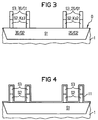
- a typical layout of a NAND gate is shown.
- German patent DE 43 41 667 C1 a NAND gate is used described, in which two parallel connected vertical MOS transistors in a common layer sequence are realized, and layer sequences of two series connected vertical MOS transistors arranged one above the other are.
- the invention is based on the problem of a circuit arrangement with at least four transistors that are improved with Circuit properties can be produced, specify. Further is a method for producing such a circuit arrangement can be specified.
- the four Transistors vertical MOS transistors.
- a first of the transistors and a fourth of the transistors are complementary to a second of the transistors and a third transistor.
- the first transistor and the fourth transistor are in series and between a first voltage connection and a Output voltage connection switched.
- the second transistor and the third transistor are connected in parallel and between the output voltage terminal and a second Voltage connection switched.
- a gate electrode of the third Transistor and a gate electrode of the fourth transistor are connected to a first input voltage connection.
- a gate electrode of the first transistor and a gate electrode of the second transistor are connected to a second input voltage connection connected.
- They are layer structures provided the channel layers of the transistors and at least include a source / drain region of each transistor.
- the Layer structures have flanks to which the channel layers border and at least in the area of the channel layers are provided with a gate dielectric to which the gate electrodes adjoin the transistors.
- the channel layer of the first transistor and the channel layer of the fourth transistor are at the same height.
- the channel layer of the second transistor and the channel layer of the third transistor are at the same height.
- the channel layer of the first transistor and the channel layer of the second transistor are at different heights.
- the circuit arrangement can be made from a single layer sequence with just four layers. In this case border one of the layers that make up the channel layers of the first and the fourth transistor, and one of the layers, which are the channel layers of the second and third transistors includes, to each other.
- a small number of layers offers the advantage that the doping profiles of the layers are less melt.
- the layer structures on both sides i.e. at least on two opposite flanks of the Layer structure, with the gate dielectric and the gate electrode be provided.
- the layer structures on both sides i.e. at least on two opposite flanks of the Layer structure, with the gate dielectric and the gate electrode be provided.
- the gate dielectric and the gate electrode be provided in contrast to a one-sided arrangement.
- the bilateral arrangement is in the bilateral arrangement without the area of the vertical MOS transistors is increased, their channel width doubled and thus the current increased and the formation of space charge zones between the two Flanks in the channel layer enlarged.
- This is beneficial since no leakage currents in space charge zones due to a parasitic Bipolar transistors arise. Because of this, it is also beneficial if located within the entire channel layer forms a space charge zone.
- the layer sequence can be generated over the entire surface of a surface of a substrate by epitaxially growing in-situ doped semiconductor material.
- a depression can also be produced in the substrate, in which the layer sequence is generated by epitaxial growth.
- a material can also be deposited on the surface in which a depression is produced which extends to the surface and in which the layer sequence is produced by epitaxial growth.
- facets form at the edges of the depression, since the growth rate at the selective epitaxy is lower at these edges.
- the layers become particularly thin, which leads to a particularly small channel length.
- Layers of the layer sequence can also be generated by implantation with differently charged ions and different ranges. Epitaxial growth is not necessary for these layers and the substrate is structured for the layer structure.
- the layer sequence can contain a silicon layer and / or an Si (1-x) Ge x layer.
- the first transistor and the fourth transistor do not match each other are complementary, the first transistor and the fourth transistor is manufactured in the same process steps what a process simplification means. The same thing applies analogously to the second transistor and the third Transistor.
- At least four of e.g. alternating conductivity types doped layers generated. If the layer sequence consists of more than four layers, must have the conductivity types of adjacent layers not be opposite.
- Complementary transistors are related to an axis that is perpendicular to the Surface of the substrate runs at different heights educated. That means that at least two of the four Layers of both channel layers and source / drain regions arise.
- More than four layers can also be formed.
- the layer structure is created using a spacer as a mask generated, an edge is formed along which by deposition and etching back the material of the spacers.
- the Edge can be created by depositing and structuring a first Auxiliary layer above the layer sequence are generated. The Edge can also be masked by etching the layer sequence arise.
- Layer structures of mutually complementary vertical MOS transistors are formed by putting a first mask on applied the layer sequence, and then at least is etched two layers thick. This creates one Layer structure and a preliminary layer structure. Then the first mask is removed. The layer structure is then covered with a second mask. Then one Layer thickness deeply etched, which creates a layer structure, which is one layer deeper than the covered one Layer structure.
- an area in which one of the Layer structures are to be generated through the second mask are covered and then a layer thickness deep silicon be etched.
- the second mask is removed.
- the first mask for generating the Layer structures is applied.
- a first first mask can first be used to form a first of the layer structures are generated.
- the first the first mask is covered by a second mask.
- a layer thickness is etched deep.
- the second mask will then cover the area not covered a second first mask for a second of the layer structures educated.
- the second mask is made of a different material than the first masks formed and after creating the second Mask removed. Then at least two layer thicknesses deeply etched, which creates the layer structures.
- layer thicknesses are essentially the same the layers expedient.
- the first mask is e.g. from four separate ones Divide. To increase the packing density and to simplify the process electrical connections can be made, in that the four layer structures are partially or completely connected. If layer structures are completely connected, that is the first mask less than four parts. Is that related of layer structures not desirable, so can, with less as a four-part first mask, the layer structures be separated from each other later.
- a first source / drain region of the second transistor and a first source / drain region of the third transistor connected to the second voltage terminal are connected, arranged above the associated channel layers are.
- This allows the layer from which a second Source / drain region of the second transistor and a second Source / drain region of the third transistor arise as electrical connection between these source / drain regions to serve.
- To connect the first source / drain regions of the second transistor and the third transistor becomes a conductive structure generated. Instead, the first source / drain region of the second transistor and the first source / drain region of the third transistor below the associated one Channel layers are arranged.
- the second source / drain region of the third Transistor and a second source / drain region of the fourth Transistor connected to the output voltage terminal are to extend beyond the transistors and to form a stage.
- the layer from which the second source / drain region of the fourth transistor is formed, to the layer from which the second source / drain region of the third transistor arises.
- a Contact of the output voltage connection arranged. The process effort decreases because of the connection of the second Source / drain regions of the second transistor, the third Transistor and the fourth transistor no additional Lines are needed.
- a first source / drain region of the fourth transistor with the second source / drain region of the first transistor via a conductive Linking structure with equally deep contacts will be second source / drain region of the first transistor above the channel layer of the first transistor.
- a contact the first voltage connection is formed on the layer, from which the first source / drain region of the first transistor arises.
- the second source / drain regions of the second transistor, of the third transistor and the fourth transistor connected differently, e.g. about a senior Structure, may be the first source / drain region of the fourth Transistor below the channel layer of the fourth transistor and the second source / drain region of the first transistor arranged below the channel layer of the first transistor become.
- the connection between the first source / drain region of the fourth transistor and the second source / drain region of the first transistor then happens over the layer from which they originated.
- a connecting line, the first Transistor with the second transistor, the second transistor with the third transistor, the third transistor with the fourth transistor and the fourth transistor with the first Transistor connects, is substantially square.
- the contact of the first input voltage connection between the third transistor and the fourth Transistor and a contact of the second input voltage terminal between the first transistor and the second Transistor are arranged.
- Other arrangements, such as along a line are also conceivable.
- the gate electrodes are spacers because the gate electrodes become small and self-aligned can be generated. This is done with conductive material deposited and then etched until the gate electrodes arise as a spacer.
- the layer structure of the first transistor and the Layer structure of the second transistor or the Layer structure of the third transistor and the layer structure of the fourth transistor at a short distance from each other to create.
- a Mask used that the first layer structure and the second Layer structure or the third layer structure and the fourth Layer structure somewhat overlapped. The conductive material under this mask forms the contact areas. It also connects it the gate electrodes of the third transistor and the fourth transistor or the gate electrodes of the first transistor and the second transistor with each other.
- the four transistors of the circuit arrangement are special suitable as a NAND gate. Because more connections to others Elements of the circuit arrangement are possible, it must be the four transistors are not necessarily a NAND gate act.
- an approximately 300 nm-thick p-doped first layer S1 is produced in a substrate 1 made of silicon.
- the dopant concentration of the first layer is approximately 10 21 cm -3 .
- An n-doped second layer S2, a p-doped third layer S3 and an n-doped fourth layer S4 are then produced on a surface O of the substrate 1 by epitaxial growth.
- the dopant concentrations of the second layer S2, the third layer S3 and the fourth layer S4 are each approximately 10 18 cm -3 .
- the second layer S2, the third layer S3 and the fourth layer S4 are each approximately 200 nm thick.
- the dopant concentration of the fourth layer S4 is then increased to 10 21 cm -3 by implantation.
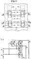
- a first auxiliary layer H1 is produced by depositing SiO 2 in a thickness of approximately 200 nm. With the aid of a second photoresist mask (not shown), which does not cover a first elongated rectangular area B1 and an elongated rectangular second area B2 running parallel thereto, SiO 2 is etched until the fourth layer S4 is partially exposed. This creates a first edge Kn1 on the edges of the first area B1 and second edges Kn2 on the edges of the second area B2.
- the first area B1 and the second area B2 are each approximately 400 nm wide with respect to an x-axis x running parallel to the surface O and 2400 nm long with respect to a y-axis y running parallel to the surface O and perpendicular to the x-axis x.
- a connecting line between a center point of the first area B1 and a center point of the second area B2 runs parallel to the x-axis (see FIG. 8).
- the structured first auxiliary layer H1 is then removed by etching with, for example, NH 4 F / HF.
- the first spacer Sp1 and the second spacer Sp2 are formed using a third photoresist mask (not shown) which has a rectangular third region B3 which overlaps the first region B1 and a rectangular fourth which overlaps the second region B2 Area B4 not covered, partially removed.
- the structured first spacer Sp1 and the structured second spacer Sp2 together form a first mask.
- Parts of the fourth layer S4 and the third layer S3 are subsequently removed by etching silicon selectively to silicon nitride with, for example, HBr / NF 3 / He / O 2 .
- a second mask M2 which overlaps half of the first region B1 and half of the second region B2, is then produced by depositing SiO 2 and structuring it by means of a photolithographic process. Using, for example, Cl 2 / CHF 3 as an etchant, silicon is selectively etched to SiO 2 until the second layer S2 is removed at unprotected locations. As a result, a second layer structure St2 and a third layer structure St3 arise from the provisional second layer structure and from the provisional third layer structure (see FIG. 2, FIG. 3 and FIG. 9).
- the second mask M2 is partially extended laterally beyond the first region B1 to the first layer S1, which is why a step Stu is formed from the first layer S1 and the second layer S2 (see FIG. 9).
- the second mask M2 is extended beyond the second area B2.
- the protected parts of the second layer S2 which are located outside the first region B1 and the second region B2 through the second mask M2 serve as electrical connections.
- the implantation increases the dopant concentration of the third layer S3 in the second layer structure St2 and the third layer structure St3 to approximately 10 21 cm -3 .
- the second mask M2 is retained.
- the second mask M2 is subsequently removed by etching with, for example, HF.
- Silicon nitride is then deposited to a thickness of approximately 80 nm (see FIG. 4).
- a third mask (not shown) is generated, the fifth regions B5, in which the first transistor, the second transistor, the third transistor and the fourth transistor are produced, are not covered (see FIG. 10 ).
- CF 4 / CHF 3 / He silicon nitride is selectively etched to SiO 2 and silicon, whereby a first insulating structure I1 is formed, which is spacer-shaped in the fifth regions B5 and conforms outside the fifth regions B5 (see FIGS. 4 and Fig. 5).
- a second insulating structure I2 is formed by thermal oxidation with a low temperature budget at a temperature of approximately 600 ° C. and a pressure of approximately 10 6 Pa (see FIG. 5). Silicon nitride is then wet-etched with, for example, H 3 PO, and the third mask is removed by wet-etching with, for example, HF. A gate dielectric Gd is grown by thermal oxidation. The gate dielectric Gd is formed at locations where parts of the first insulating structure I1 were located within the fifth regions B5.
- Polysilicon doped in situ is then deposited.
- a fourth photoresist mask MF4 which essentially covers the third region B3 and the fourth region B4 (see FIG. 10)
- polysilicon is etched with, for example, Cl 2 / CHF 3 , as a result of which a spacer-shaped first is located on opposite flanks of the first layer structure St1
- Gate electrode Ga1 a spacer-shaped second gate electrode Ga2 on opposite flanks of the second layer structure St2
- Polysilicon under the fourth photoresist mask MF4 serves as the first contact area, which connects the third gate electrode Ga3 to the fourth gate electrode Ga4, and as the second contact area, which connects the first gate electrode Ga1 to the second gate electrode Ga2.
- a first contact K1 is created later on the first contact surface and a second contact K2 is generated on the second contact surface.
- the second insulating structure I2 reduces capacities through the first gate electrode Ga1 and the second layer S2, through the second gate electrode Ga2 and the first layer S1, through the third gate electrode Ga3 and the first layer S1, and through the fourth gate electrode Ga4 and the second Layer S2 are formed.
- the dimensions of the first area B1 and the second area B2 were chosen so that polysilicon after etching these areas are essentially covered (see FIG. 6).
- SiO 2 is deposited in a thickness of approx. 300 nm and etched back with, for example, Cl 2 / CHF 3 , whereby a third insulating structure I3 is generated, which comprises the first gate electrode Ga1, the second gate electrode Ga2, the third gate electrode Ga3 and the fourth Gate electrode Ga4, covered.
- Silicon nitride is then deposited to a thickness of approximately 200 nm. With the help of a fifth photoresist mask (not shown), depressions are created for contacts.
- CF 4 / CHF 3 / H 2 silicon nitride is selectively etched to SiO 2 .
- the third insulating structure I3 made of SiO 2 serves as an etch stop.
- a depression up to the first contact surface is produced for the first contact K1.
- a depression up to the second contact surface is produced for the second contact K2.
- a recess is created which overlaps the Stu step.
- a depression up to a part of the second layer S2, which serves as an electrical connection to the first source / drain region of the first transistor is produced in a location originally covered by the second mask M2.
- a depression up to the first source / drain region of the third transistor is produced for a fifth of the contacts K5.
- a depression up to the first source / drain region of the second transistor is produced for a sixth of the contacts K6.
- a depression up to the first source / drain region of the fourth transistor is produced for a seventh of the contacts K7.
- a depression is produced up to the second source / drain region of the first transistor.
- Titanium is deposited in a thickness of approx. 100 nm and selectively siliconized, which creates contact structures Ks. Remaining titanium is removed with, for example, CCl 2 F 2 / NF 3 .
- Aluminum is deposited in a thickness of approx. 400 nm, which creates the contacts K1, K2, K3, K4, K5, K6, K7, K8.
- the aluminum is then structured so that a first conductive structure L1 is generated, the seventh Contact K7 and the eighth contact K8 connects to each other and a second conductive structure L2 is created which corresponds to the fifth contact K5 and sixth contact K6 with each other connects (see Figure 6).
- the four transistors form a NAND gate (see Figure 12).
- the first contact K1 is connected to a first input voltage connection U IN1 .
- the second contact K2 is connected to a second input voltage connection U IN2 .
- the third contact K3 is connected to an output voltage connection U OUT .
- the fourth contact K4 is connected to a first voltage connection U SS .
- the second conductive structure L2 is connected to a second voltage connection U DD .
- the second isolating structure can also be generated by a deposition process.
- Insulating structures can also be made from other insulating ones Materials are created. Leave instead of doped polysilicon also e.g. Use metal silicides and / or metals.
Landscapes
- Metal-Oxide And Bipolar Metal-Oxide Semiconductor Integrated Circuits (AREA)
- Read Only Memory (AREA)
- Bipolar Transistors (AREA)
- Thin Film Transistor (AREA)
Applications Claiming Priority (2)
| Application Number | Priority Date | Filing Date | Title |
|---|---|---|---|
| DE19736672 | 1997-08-22 | ||
| DE19736672 | 1997-08-22 |
Publications (3)
| Publication Number | Publication Date |
|---|---|
| EP0899783A2 true EP0899783A2 (fr) | 1999-03-03 |
| EP0899783A3 EP0899783A3 (fr) | 2000-08-16 |
| EP0899783B1 EP0899783B1 (fr) | 2008-04-16 |
Family
ID=7839912
Family Applications (1)
| Application Number | Title | Priority Date | Filing Date |
|---|---|---|---|
| EP98115375A Expired - Lifetime EP0899783B1 (fr) | 1997-08-22 | 1998-08-14 | Arrangement de circuit comportant au moins quatre transistors et procédé de fabrication |
Country Status (6)
| Country | Link |
|---|---|
| US (1) | US6060911A (fr) |
| EP (1) | EP0899783B1 (fr) |
| JP (1) | JPH11145309A (fr) |
| KR (1) | KR100547400B1 (fr) |
| DE (1) | DE59814218D1 (fr) |
| TW (1) | TW423116B (fr) |
Cited By (2)
| Publication number | Priority date | Publication date | Assignee | Title |
|---|---|---|---|---|
| WO2000046855A1 (fr) * | 1999-02-03 | 2000-08-10 | France Telecom | Dispositif semi-conducteur de portes logiques non-et ou non-ou a n entrees, et procede de fabrication correspondant |
| EP1063697A1 (fr) * | 1999-06-18 | 2000-12-27 | Lucent Technologies Inc. | Circuit intégré CMOS comportant des transistors verticaux et son procédé de fabrication |
Families Citing this family (5)
| Publication number | Priority date | Publication date | Assignee | Title |
|---|---|---|---|---|
| DE59814314D1 (de) * | 1997-07-18 | 2008-12-11 | Infineon Technologies Ag | Verfahren zur herstellung eines vertikalen mos-transistors |
| JP2007220808A (ja) * | 2006-02-15 | 2007-08-30 | Toshiba Corp | 半導体装置及びその製造方法 |
| US7838948B2 (en) * | 2007-01-30 | 2010-11-23 | Infineon Technologies Ag | Fin interconnects for multigate FET circuit blocks |
| JP5635256B2 (ja) | 2009-11-24 | 2014-12-03 | ピーエスフォー ルクスコ エスエイアールエルPS4 Luxco S.a.r.l. | 半導体装置及びその製造方法 |
| US12236293B1 (en) | 2024-01-24 | 2025-02-25 | Morgan Stanley Services Group Inc. | Systems and methods for mainframe messaging abstraction framework |
Family Cites Families (14)
| Publication number | Priority date | Publication date | Assignee | Title |
|---|---|---|---|---|
| US4951102A (en) * | 1988-08-24 | 1990-08-21 | Harris Corporation | Trench gate VCMOS |
| US5032529A (en) * | 1988-08-24 | 1991-07-16 | Harris Corporation | Trench gate VCMOS method of manufacture |
| DE3838355A1 (de) * | 1988-11-11 | 1990-05-17 | Fraunhofer Ges Forschung | Vertikaltransistoranordnung |
| JP2991489B2 (ja) * | 1990-11-30 | 1999-12-20 | 株式会社東芝 | 半導体装置 |
| US5208172A (en) * | 1992-03-02 | 1993-05-04 | Motorola, Inc. | Method for forming a raised vertical transistor |
| US5252849A (en) * | 1992-03-02 | 1993-10-12 | Motorola, Inc. | Transistor useful for further vertical integration and method of formation |
| US5612563A (en) * | 1992-03-02 | 1997-03-18 | Motorola Inc. | Vertically stacked vertical transistors used to form vertical logic gate structures |
| US5340754A (en) * | 1992-09-02 | 1994-08-23 | Motorla, Inc. | Method for forming a transistor having a dynamic connection between a substrate and a channel region |
| US5324673A (en) * | 1992-11-19 | 1994-06-28 | Motorola, Inc. | Method of formation of vertical transistor |
| DE4341667C1 (de) * | 1993-12-07 | 1994-12-01 | Siemens Ag | Integrierte Schaltungsanordnung mit mindestens einem CMOS-NAND-Gatter und Verfahren zu deren Herstellung |
| KR100193102B1 (ko) * | 1994-08-25 | 1999-06-15 | 무명씨 | 반도체 장치 및 그 제조방법 |
| US5581101A (en) * | 1995-01-03 | 1996-12-03 | International Business Machines Corporation | FET and/or bipolar devices formed in thin vertical silicon on insulator (SOI) structures |
| US5872374A (en) * | 1996-03-29 | 1999-02-16 | Motorola, Inc. | Vertical semiconductor device |
| US5923185A (en) * | 1997-03-12 | 1999-07-13 | Xilinx, Inc. | Logic circuit programmable to implement at least two logic functions |
-
1998
- 1998-08-03 TW TW087112741A patent/TW423116B/zh not_active IP Right Cessation
- 1998-08-14 DE DE59814218T patent/DE59814218D1/de not_active Expired - Lifetime
- 1998-08-14 EP EP98115375A patent/EP0899783B1/fr not_active Expired - Lifetime
- 1998-08-19 JP JP23314198A patent/JPH11145309A/ja not_active Withdrawn
- 1998-08-21 US US09/138,160 patent/US6060911A/en not_active Expired - Lifetime
- 1998-08-21 KR KR1019980033909A patent/KR100547400B1/ko not_active Expired - Fee Related
Cited By (2)
| Publication number | Priority date | Publication date | Assignee | Title |
|---|---|---|---|---|
| WO2000046855A1 (fr) * | 1999-02-03 | 2000-08-10 | France Telecom | Dispositif semi-conducteur de portes logiques non-et ou non-ou a n entrees, et procede de fabrication correspondant |
| EP1063697A1 (fr) * | 1999-06-18 | 2000-12-27 | Lucent Technologies Inc. | Circuit intégré CMOS comportant des transistors verticaux et son procédé de fabrication |
Also Published As
| Publication number | Publication date |
|---|---|
| TW423116B (en) | 2001-02-21 |
| DE59814218D1 (de) | 2008-05-29 |
| KR100547400B1 (ko) | 2006-03-23 |
| KR19990023755A (ko) | 1999-03-25 |
| JPH11145309A (ja) | 1999-05-28 |
| US6060911A (en) | 2000-05-09 |
| EP0899783A3 (fr) | 2000-08-16 |
| EP0899783B1 (fr) | 2008-04-16 |
Similar Documents
| Publication | Publication Date | Title |
|---|---|---|
| DE69121535T2 (de) | Feldeffekttransistor mit inverser T-förmiger Silizid-Torelektrode | |
| DE69005129T2 (de) | Verfahren zur Herstellung von integrierten Schaltungen mit EPROM-Speicher-Transistoren und logischen Transistoren. | |
| DE10141916A1 (de) | MOS-Halbleitervorrichtung und Verfahren zum Herstellen derselben | |
| EP0118709A2 (fr) | Procédé pour la fabrication de transistor MOS à régions de source et drain planaires, à courte longueur de canal et à niveau de contact auto-aligné comportant un siliciure métallique | |
| DE102012214077A1 (de) | Integrierte Schaltungen mit abstehenden Source- und Drainbereichen und Verfahren zum Bilden integrierter Schaltungen | |
| DE68905487T2 (de) | Verfahren zur herstellung einer integrierten schaltung mit bauelementen, die gates auf zwei ebenen enthalten. | |
| DE19853268C2 (de) | Feldeffektgesteuerter Transistor und Verfahren zu dessen Herstellung | |
| DE19501557A1 (de) | Halbleitervorrichtung und Verfahren zu deren Herstellung | |
| DE10107012A1 (de) | Verfahren zur Herstellung eines Polysilicium-Kondensators unter Verwendung von FET- und bipolaren Basis-Polysiliciumschichten | |
| DE19720193C2 (de) | Integrierte Schaltungsanordnung mit mindestens zwei vertikalen MOS-Transistoren und Verfahren zu deren Herstellung | |
| WO2000019527A1 (fr) | Configuration de cellules dram et son procede de production | |
| EP0899783B1 (fr) | Arrangement de circuit comportant au moins quatre transistors et procédé de fabrication | |
| DE69509698T2 (de) | Verfahren zur Herstellung eines Feldeffekttransistors mit isoliertem Gate und kurzem Kanal, und entsprechender Transistor | |
| EP0920060B1 (fr) | Réseau de cellules SRAM et méthode de fabrication | |
| DE19746900C2 (de) | Vertikaler MOS-Transistor und Verfahren zu dessen Herstellung | |
| DE3119137A1 (de) | Halbleiter und verfahren zu deren herstellung | |
| DE112006001520B4 (de) | Prozess für die Herstellung erhabener Source- und Drain-Gebiete mit zu entfernenden Abstandshaltern, wobei "Mausohren" vermieden werden | |
| DE69207973T2 (de) | Verfahren zum Herstellen eines vertikalen Feldeffekt-Transistors und durch dieses Verfahren hergestellter Transistor | |
| DE2738049A1 (de) | Integrierte halbleiterschaltungsanordnung | |
| DE3280420T2 (de) | Verfahren zum herstellen eines mos-transistors auf einem substrat. | |
| DE19845066C2 (de) | Integrierte Schaltungsanordnung und Verfahren zu deren Herstellung | |
| DE19836953B4 (de) | MOSFET und Verfahren zu seiner Herstellung | |
| EP0996982B1 (fr) | Procede pour la fabrication d'un transistor mos vertical | |
| DE2806410A1 (de) | Halbleiteranordnung und verfahren zu deren herstellung | |
| WO2001018873A1 (fr) | Transistor mos et son procede de production |
Legal Events
| Date | Code | Title | Description |
|---|---|---|---|
| PUAI | Public reference made under article 153(3) epc to a published international application that has entered the european phase |
Free format text: ORIGINAL CODE: 0009012 |
|
| AK | Designated contracting states |
Kind code of ref document: A2 Designated state(s): DE FR GB IT |
|
| AX | Request for extension of the european patent |
Free format text: AL;LT;LV;MK;RO;SI |
|
| PUAL | Search report despatched |
Free format text: ORIGINAL CODE: 0009013 |
|
| AK | Designated contracting states |
Kind code of ref document: A3 Designated state(s): AT BE CH CY DE DK ES FI FR GB GR IE IT LI LU MC NL PT SE |
|
| AX | Request for extension of the european patent |
Free format text: AL;LT;LV;MK;RO;SI |
|
| 17P | Request for examination filed |
Effective date: 20000904 |
|
| AKX | Designation fees paid |
Free format text: DE FR GB IT |
|
| RAP1 | Party data changed (applicant data changed or rights of an application transferred) |
Owner name: INFINEON TECHNOLOGIES AG |
|
| 17Q | First examination report despatched |
Effective date: 20060721 |
|
| GRAP | Despatch of communication of intention to grant a patent |
Free format text: ORIGINAL CODE: EPIDOSNIGR1 |
|
| RAP1 | Party data changed (applicant data changed or rights of an application transferred) |
Owner name: QIMONDA AG |
|
| GRAS | Grant fee paid |
Free format text: ORIGINAL CODE: EPIDOSNIGR3 |
|
| GRAA | (expected) grant |
Free format text: ORIGINAL CODE: 0009210 |
|
| AK | Designated contracting states |
Kind code of ref document: B1 Designated state(s): DE FR GB IT |
|
| REF | Corresponds to: |
Ref document number: 59814218 Country of ref document: DE Date of ref document: 20080529 Kind code of ref document: P |
|
| PLBE | No opposition filed within time limit |
Free format text: ORIGINAL CODE: 0009261 |
|
| STAA | Information on the status of an ep patent application or granted ep patent |
Free format text: STATUS: NO OPPOSITION FILED WITHIN TIME LIMIT |
|
| EN | Fr: translation not filed | ||
| 26N | No opposition filed |
Effective date: 20090119 |
|
| GBPC | Gb: european patent ceased through non-payment of renewal fee |
Effective date: 20080814 |
|
| PG25 | Lapsed in a contracting state [announced via postgrant information from national office to epo] |
Ref country code: IT Free format text: LAPSE BECAUSE OF FAILURE TO SUBMIT A TRANSLATION OF THE DESCRIPTION OR TO PAY THE FEE WITHIN THE PRESCRIBED TIME-LIMIT Effective date: 20080416 |
|
| PG25 | Lapsed in a contracting state [announced via postgrant information from national office to epo] |
Ref country code: GB Free format text: LAPSE BECAUSE OF NON-PAYMENT OF DUE FEES Effective date: 20080814 |
|
| PG25 | Lapsed in a contracting state [announced via postgrant information from national office to epo] |
Ref country code: FR Free format text: LAPSE BECAUSE OF FAILURE TO SUBMIT A TRANSLATION OF THE DESCRIPTION OR TO PAY THE FEE WITHIN THE PRESCRIBED TIME-LIMIT Effective date: 20090227 |
|
| REG | Reference to a national code |
Ref country code: DE Ref legal event code: R081 Ref document number: 59814218 Country of ref document: DE Owner name: POLARIS INNOVATIONS LTD., IE Free format text: FORMER OWNER: QIMONDA AG, 81739 MUENCHEN, DE Ref country code: DE Ref legal event code: R081 Ref document number: 59814218 Country of ref document: DE Owner name: INFINEON TECHNOLOGIES AG, DE Free format text: FORMER OWNER: QIMONDA AG, 81739 MUENCHEN, DE |
|
| REG | Reference to a national code |
Ref country code: DE Ref legal event code: R081 Ref document number: 59814218 Country of ref document: DE Owner name: POLARIS INNOVATIONS LTD., IE Free format text: FORMER OWNER: INFINEON TECHNOLOGIES AG, 85579 NEUBIBERG, DE |
|
| PGFP | Annual fee paid to national office [announced via postgrant information from national office to epo] |
Ref country code: DE Payment date: 20150929 Year of fee payment: 18 |
|
| REG | Reference to a national code |
Ref country code: DE Ref legal event code: R119 Ref document number: 59814218 Country of ref document: DE |
|
| PG25 | Lapsed in a contracting state [announced via postgrant information from national office to epo] |
Ref country code: DE Free format text: LAPSE BECAUSE OF NON-PAYMENT OF DUE FEES Effective date: 20170301 |