EP0902543B1 - Verfahren und Gerät zur Digitalwandlung von Winkeln - Google Patents
Verfahren und Gerät zur Digitalwandlung von Winkeln Download PDFInfo
- Publication number
- EP0902543B1 EP0902543B1 EP97310199A EP97310199A EP0902543B1 EP 0902543 B1 EP0902543 B1 EP 0902543B1 EP 97310199 A EP97310199 A EP 97310199A EP 97310199 A EP97310199 A EP 97310199A EP 0902543 B1 EP0902543 B1 EP 0902543B1
- Authority
- EP
- European Patent Office
- Prior art keywords
- sin
- cos
- output
- digital angle
- signal
- Prior art date
- Legal status (The legal status is an assumption and is not a legal conclusion. Google has not performed a legal analysis and makes no representation as to the accuracy of the status listed.)
- Expired - Lifetime
Links
- 238000006243 chemical reaction Methods 0.000 title claims description 20
- 230000001360 synchronised effect Effects 0.000 claims description 25
- 238000000034 method Methods 0.000 claims description 23
- 230000010356 wave oscillation Effects 0.000 claims description 4
- 238000010586 diagram Methods 0.000 description 12
- 238000001514 detection method Methods 0.000 description 9
- 238000012546 transfer Methods 0.000 description 7
- 230000005284 excitation Effects 0.000 description 6
- 239000004065 semiconductor Substances 0.000 description 4
- 239000003990 capacitor Substances 0.000 description 3
- 230000008859 change Effects 0.000 description 3
- 230000007423 decrease Effects 0.000 description 3
- 101100521334 Mus musculus Prom1 gene Proteins 0.000 description 2
- 229920005994 diacetyl cellulose Polymers 0.000 description 2
- 230000006872 improvement Effects 0.000 description 2
- 230000008569 process Effects 0.000 description 2
- 230000002411 adverse Effects 0.000 description 1
- 230000015572 biosynthetic process Effects 0.000 description 1
- 230000000295 complement effect Effects 0.000 description 1
- 239000000470 constituent Substances 0.000 description 1
- 230000003247 decreasing effect Effects 0.000 description 1
- 238000011161 development Methods 0.000 description 1
- 238000007599 discharging Methods 0.000 description 1
- 238000002474 experimental method Methods 0.000 description 1
- 230000004907 flux Effects 0.000 description 1
- 230000014509 gene expression Effects 0.000 description 1
- 230000004048 modification Effects 0.000 description 1
- 238000012986 modification Methods 0.000 description 1
- 230000010355 oscillation Effects 0.000 description 1
- 230000004044 response Effects 0.000 description 1
- 238000003786 synthesis reaction Methods 0.000 description 1
Images





Classifications
-
- H—ELECTRICITY
- H03—ELECTRONIC CIRCUITRY
- H03M—CODING; DECODING; CODE CONVERSION IN GENERAL
- H03M1/00—Analogue/digital conversion; Digital/analogue conversion
- H03M1/12—Analogue/digital converters
- H03M1/48—Servo-type converters
- H03M1/485—Servo-type converters for position encoding, e.g. using resolvers or synchros
Definitions
- the present invention relates to a digital angle conversion method and, more particularly, to novel improvement of conversion of a tracking method for making respective circuit arrangements as a monolithic semiconductor and achieving a low price, a small size, a light weight, high reliability, and high-speed tracking.
- FIG. 1 As a conventionally used digital angle conversion method of this type, for example, a tracking method shown in FIG. 1 is popularly used. More specifically, reference numeral 100 in FIG. 1 denotes a resolver excited by an exciting signal E ⁇ sin ⁇ t. Two-phase outputs KEsin ⁇ sin ⁇ t and KEcos ⁇ sin ⁇ t obtained from the resolver 100 are arithmetically operated by an arithmetic operator 101. The output signal KEsin ⁇ t ⁇ sin( ⁇ - ⁇ ) (where ⁇ : resolver rotating angle, and ⁇ : output counter value) is synchronously rectified by a synchronous rectifier 102 to which the exciting signal E ⁇ sin ⁇ t is input.
- the output signal KEsin( ⁇ - ⁇ ) obtained by the synchronous rectifier 102 is input to a counter 103 as a pulse output 104a through a voltage controlled oscillator 104 to obtain an output counter value ⁇ serving as a digital angle output from the counter 103.
- the output counter value ⁇ is fed back to form a feedback loop. Therefore, when a velocity signal 105 is obtained by the output signal KEsin( ⁇ - ⁇ ) from the synchronous rectifier 102, and a position signal 106 can be obtained by the output counter value ⁇ from the counter 103.
- the digital analog conversion method Since the conventional digital angle conversion method is arranged as described above, the digital analog conversion method has the following problem.
- the block diagram since partially constituted by a complex analog block diagram, the block diagram cannot be made as a monolithic semiconductor as a whole, a low price, a small size, a light weight, high reliability, and utility cannot be easily achieved. In addition, a preferable means for improving a tracking speed cannot be found.
- the synchro-to-digital converter produces an rotating signal.
- the rotating signals are applied to a synchronous demodulator which receives the excitation signal and which demodulates the rotating signal to produce a substantially sinusoidal waveforms (COS ⁇ and SIN ⁇ ).
- COS ⁇ and SIN ⁇ substantially sinusoidal waveforms
- These substantially sinusoidal waveforms are applied to the analog inputs of multiplying digital-to-analog converter circuits.
- the digital inputs to these D/A converters are driven by 12-bit binary numbers read from PROMs. These binary numbers correspond to the amplitudes SIN ⁇ and COS ⁇ , where ⁇ is the resolver rotor angle as measured by the circuit.
- the analog signal (SIN ⁇ COS ⁇ ) which is produced by one of the D/A converters is subtracted from the analog signal (COS ⁇ SIN ⁇ ) produced by the other D/A converter. This subtraction is performed by an operational amplifier which produces an analog error signal SIN( ⁇ - ⁇ ).
- This error signal is integrated by an integrator circuit and it is applied to the input of a voltage controlled oscillator (VCO).
- VCO produces "UP" pulses when the measured angle ⁇ is less than the actual rotor angle ⁇ , and it produces “DOWN” pulses when the measured angle ⁇ is greater.
- the 12-bit counter thus stores a number which tracks the actual rotor angle ⁇ , and its output is a binary number which equals the measured rotor angle ⁇ . This number is applied to a bus which connects to the address terminals on the PROMs to close the loop and thereby force the meaured angel ⁇ to follow the actual rotor angle ⁇ .
- GB 2,242,583 discloses a tracking resolver to digital converter in which cosine and sine resolver inputs are multiplied with digital sine and cosine internal signals in respective DACs, and the outputs are fed into an error amplifier which produces an error signal.
- the error signal is demodulated and then fed into an accurnulator.
- the accumulator output is first fed into a cos look-up table and then a sin look-up table to produce respective input signals for the DACs.
- US 4,149,260 discloses a system for determining the value of an angle represented by first and second analogue signals which are a function of sin and cos of the angle. Angle computation is performed as a function of the ratio of the number of complete half cycles of the demodulated signals during a fixed time interval plus the change in the output of the integrator since the previous time interval.
- the present invention has been made to solve the above problem and, more particularly, has as its object to provide a digital angle conversion method which makes respective circuit arrangements as a monolithic semiconductor, achieves a low price, a small size, a light weight, and high reliability, and makes it possible to obtain high-speed tracking.
- reference numeral 1 denotes, e.g., a known one-phase excitation/two-phase output type resolver 1
- two-phase rotating signals sin ⁇ f(t) and cos ⁇ f(t) including an exciting component f(t) output from the resolver 1 are input from a SIN ⁇ COS multiplier 2 to a synchronous detector 3 as a first output signal sin( ⁇ - ⁇ ) ⁇ f(t), and a second output signal sin( ⁇ - ⁇ ) from the synchronous detector 3 is input to a voltage controlled oscillator through an integrator 4.
- An up pulse 5a and a down pulse 5b from the voltage controlled oscillator 5 are counted by a one-turn counter 6 as a CW direction or a CCW direction to output a digital angle output ⁇ .
- a carry signal CA and a borrow signal BO from the one-turn counter 6 are input to a multi-turn counter 7, and a multi-turn signal MT from the multi-turn counter 7 is transmitted to an external circuit through a multi-turn data processor 8 and a bus interface 9 together with the digital angle output ⁇ .
- the digital angle output ⁇ is input, through a path 10, to a synchronous phase detector 11, the SIN ⁇ COS multiplier 2, and an encoder pulse generation logic section 12 to which the rotating signals sin ⁇ f(t), cos ⁇ f(t) is input.
- a known tracking scheme using feedback is formed by the path 10, and an encoder signal 13 constituted by known A, B, Z, U, V, and W is output from the encoder pulse generation logic section 12.
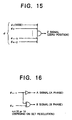
- the encoder signal 13 is obtained in the following manner. That is, as well known, when A, B, and Z signals (A phase, B phase, and Z phase representing i.e., a zero position) are extracted by converting the digital angle output ⁇ serving as an absolute digital (parallel) signal, as shown in FIG.
- the Z signal is output by using LSB to MSB of the digital angle output ⁇ , and, as shown in FIG. 16, ⁇ n-1 and ⁇ n (n: 10 or 14 depending on a set resolution) of the digital angle output ⁇ are used.
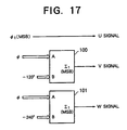
- U, V, and W signals serving as phase switching signals of a 3-phase motor are obtained in the following manner. That is, as shown in FIG. 17, ⁇ 1 (MSB) is used as the U signal, and signals having angles of -120° and -240° with respect to the digital angle output ⁇ are input to full-adder type adders 100 and 101 to obtain the V and W signals.
- the synchronous detection ON/OFF signal 13a is input to the synchronous detector 3, and a known triangular wave oscillation circuit 14 for outputting an exciting reference signal 14a constituted by a triangular wave of, e.g., 10 kHz is arranged.
- the exciting reference signal 14a is input to a known current control amplifier 15, a resolver exciting power supply output 15a output depending on the level of the exciting reference signal 14a is applied to the resolver 1 as an exciting signal REF of the resolver 1.
- the one-phase excitation/two-phase output (amplitude modification) type resolver 1 is a stable sensor which does not depend on temperature drift, a transfer cable length, or the like.
- an exciting component function of the resolver 1 is represented by f(t)
- the following two-phase sin wave signals is subjected to amplitude modulation by the angle ⁇ are output from the resolver 1.
- V s2-s4 Sin ⁇ . f(t)
- V s1-s3 Cos ⁇ . f(t)
- V S2-S4 and V S1-S3 are outputs of both the ends of the known two-phase output coil (not shown) of the resolver 1.
- the function f(t) becomes a rectangular wave (10 kHz).
- the integrator 4 serving as a constituent element of a tracking loop corresponds to a compensator in a control theory for improving the stability and responsibility of a control system, and has transfer characteristics expressed by Equation (6) of Number 2 described below.
- Equation (6) Number 2 described below.
- Gi 1 T ⁇ 1+T1 ⁇ S S(1+T2 ⁇ S) (S: Laplace operator) where Gi: transfer function of the integrator, T: integrator constant.
- the VCO voltage controlled oscillator 5 (to be described later), as well known, is means for converting an input voltage into a digital pulse, and the one-turn counter 6 is means for integrating (counting) an input pulse to convert the input pulse into a parallel digital angle signal ⁇ .
- amplitude modulation type resolver excitation controls the voltage of a sin wave.
- a current of a triangular wave (10 kHz) is controlled in the following manners.
- FIG. 3 is an equivalent circuit of the resolver.
- an exciting coil and an output coil are M-coupled with each other and relatively rotated ( ⁇ ) to each other, and an input voltage Vi of the exciting coil and an output voltage Vo of the output coil are given by Equations (7) and (8) described below as shown in FIG. 4:
- Equation (10) means a release voltage and corresponds to an input current.
- the Laplace operator (S) is equivalent to jw in an electric circuit. S ⁇ jw where Vi: exciting (input) voltage Ii: exciting (input) current Vo: output voltage Io: output current Ri: DC resistance component of exciting coil Ro: DC resistance component of output coil Li: inductance component of exciting coil Lo: inductance component of output coil M: mutual inductance
- the rotating signals sin ⁇ f(t), cos ⁇ f(t) serving as resolver output signals (Vo) have rectangular waves. Since these rectangular waves are basically directly replaced with straight lines (DC) in synchronous detection of the following stage, a filter for converting a signal into a DC voltage in a conventional sin wave excitation is not required, thereby canceling a conventional filter time constant. As a result, the response characteristics of the control system can be improved.
- the exciting component f(t) of the rotating signals sin ⁇ f(t), cos ⁇ f(t), which serve as resolver output signals, is supplied from the current control amplifier 15 to the resolver 1 through a transfer cable, converted into a resolver output signal including angle information by the resolver 1, and then input to a reception-side circuit through the transfer cable again. In any one of these processes, a phase difference is generated.
- the following method is used. That is, attentions are given to only an exciting component (having a phase difference) included in a resolver signal, and the exciting component detected (extracted) from the resolver signal itself is replaced with an original exciting signal, so that a basic phase difference is always set to zero.
- the resolver signal is subjected to amplitude modulation by the rotating angle ⁇ . For this reason, depending on the angle, an amplitude level decreases, and the exciting component is inconveniently extracted.
- an exciting component of a two-phase resolver signal must be free from a relative phase difference.
- the sin ⁇ and cos ⁇ signals of the digital angle output ⁇ required in the SIN ⁇ COS multiplier 2 are realized by approximate expressions shown in Equation (3): where 0 ⁇ ⁇ ⁇ 1 (range of 0° to 90°)
- Equation (3) a value A is calculated by an experience manner, the approximate precision of this numerical value influences the digital conversion precision itself of the system.
- Equation (3) is to approximate a sin or cos function itself.
- the approximation is performed such that the function expressed by Equation (2), i.e., the value of the control deviation expressed by Equation (4) is maximally approximated.
- Equation (3) An actual circuit for realizing Equation (3) is shown in FIG. 6.
- the basic arrangement of the circuit is a known multiplication type D/A converter, and selectively sets R1 and R2 of a feedback system to obtain the characteristics given by Equation (3).
- an arithmetic operation can be performed in the range of 0° to 90°. However, synthesis is performed such that one rotation is divided into four quadrants each having 90°, the entire range can be covered.
- sin ⁇ has monotonous increase characteristics
- cos ⁇ has monotonous decrease characteristics
- Equation (2) described above can be realized by the above combinations in the entire range.
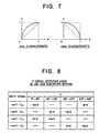
- the rotating signals sin ⁇ f(t), cos ⁇ f(t) are input to a signal selection logic 20 shown in FIG. 8 to perform a subtracting process to cos ⁇ and sin ⁇ , so that the first output signal sin( ⁇ - ⁇ ) ⁇ f(t) can be output.
- a multi-turn count detecting method will be described below.
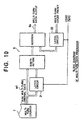
- the multi-turn detection value itself as is apparent from the principle, although it is not an absolute value, a circuit shown in FIG. 10 is added as a means for realizing an absolute value (including a multi-turn portion) in only a continuous power ON state.
- a multi-turn count adjusted to a machine shaft is preset by the latch circuits 21 and 22 in a continuous power ON state.
- An absolute value detection can be equivalently realized in the entire range.
- VCO voltage controlled oscillator
- the VCO is a pulse oscillator depending on a single-polarity analog signal input level, and the polarity of UP/DOWN is determined by another circuit.
- the VCO according to the present invention has all the above functions to achieve the simplification, stability, and high speed of the circuit.
- the above voltage controlled oscillator 5 is arranged as follows.
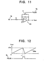
- Four comparators COMP1 to COMP4 are arranged on the output side of the voltage controlled oscillator 5A as shown in Fig. 11, and four gate circuits G1 to G4 are arranged on outputs 5d, 5e, 5f, and 5g of the comparators COMP1 to COMP4 are arranged.
- the pulse 5c from a gate circuit G5 connected between the gates G2 and G3 is applied to the switch S connected between both the ends of the feedback capacitor C, and an up pulse 5a and a down pulse 5b are output from the gate G1 and the gate G4, respectively.
- FIG. 14 A waveform chart showing the operation in FIG. 13 is shown in FIG. 14.
- Equation (14) is equivalent to Equation (1).
- a SIN ⁇ COS multiplier, a voltage controlled oscillator, a triangular wave oscillation circuit, and the like are made as a monolithic semiconductor, improvement of reliability and utility, a low price, and multi-function can be achieved. High-speed tracking can also be obtained.
Landscapes
- Engineering & Computer Science (AREA)
- Theoretical Computer Science (AREA)
- Transmission And Conversion Of Sensor Element Output (AREA)
Claims (5)
- Digitales Winkelwandlungsverfahren, bei dem ein digitaler Winkelausgang aus Drehsignalen sin·f(t) und cos·f(t) erhalten wird, die von einem sich drehenden Detektor (1) erhalten werden, wobei f(t) eine Erregersignalkomponente ist, wobei:die Drehsignale sin·f(t) und cos·f(t) einem sin·cos-Multiplizierer (2) zugeführt und jeweils mit sin und cos verarbeitet werden, die von dem digitalen Winkelausgang erhalten werden, um ein erstes Ausgangssignal sin( - )·f(t) als das Ergebnis von sin·f(t) x cos - cos·f(t) x sin = sin( - )·f(t) zu erhalten;das erste Ausgangssignal sin( - )·f(t) durch einen synchronen Detektor (3) synchron gleichgerichtet wird, um die Erregersignalkomponente f(t) zu entfernen, um so ein zweites Ausgangssignal sin( - ) zu erhalten;das zweite Ausgangssignal sin( - ) durch einen Integrator (4) und einen spannungsgesteuerten Oszillator (5) geführt wird, um den digitalen Winkelausgang von einem One-Turn-Zähler zu erhalten;der digitale Winkelausgang in den sin.cos-Multiplizierer (2) und in einen synchronen Phasendetektor (11) eingegeben wird, um eine Rückkopplungssteuerung durchzuführen, wobei eine Steuerabweichung ε = sin( - ) in dieser Rückkopplungssteuerung auf Null gesetzt wird, um = zu erfüllen; unddie Drehsignale und ein Erreger-Referenzsignal dem synchronen Phasendetektor zugeführt werden, wobei der synchrone Phasendetektor dem synchronen Detektor ein Signal zuführt.
- Digitales Winkelwandlungsverfahren nach Anspruch 1, dadurch gekennzeichnet, dass eine Dreieckwelle, die von einer Dreieckwellen-Oszillationsschaltung (14) erhalten wird, als eine Erregerkomponente f(t) verwendet wird.
- Digitales Winkelwandlungsverfahren nach Anspruch 1 oder Anspruch 2, dadurch gekennzeichnet, dass bewirkt wird, dass der digitale Winkelausgang durch einen Enkoder-Impulserzeugungs-Logikabschnitt (12) geführt wird, um Enkoder-Signale (A, B, Z, U, V und W) zu erhalten.
- Digitales Winkelwandlungsverfahren nach Anspruch 1 oder 2, dadurch gekennzeichnet, dass ein Ausgang von dem One-Turn-Zähler (6) in einen Multi-Turn-Zähler eingegeben wird, um Multi-Turn-Daten (MT) zu erhalten.
- Digitales Winkelwandlungsgerät, zu einen digitalen Winkelausgang aus Drehsignalen sin·f(t) und cos·f(t) zu erhalten, die von einem sich drehenden Detektor (1) erhalten werden, wobei f(t) eine Erregersignalkomponente ist, wobei das Gerät aufweist:einen sin·cos-Multiplizierer, wobei die Drehsignale sin·f(t) und cos·f(t) dem sin·cos-Multiplizierer (2) zugeführt und jeweils mit sin und cos verarbeitet werden, die von dem digitalen Winkelausgang erhalten werden, um ein erstes Ausgangssignal sin( - )·f(t) als das Ergebnis von sin·f(t) x cos - cos·f(t) x sin = sin( - )·f(t) zu erhalten;einen synchronen Detektor (3), um das erste Ausgangssignal sin( - )·f(t) synchron gleichzurichten, um die Erregersignalkomponente f(t) zu entfernen, um so ein zweites Ausgangssignal sin( - ) zu erhalten;einen Integrator (4), um das zweite Ausgangssignal sin( - ) zu integrieren; undeinen spannungsgesteuerten Oszillator (5), um den digitalen Winkelausgang von einem One-Turn-Zähler zu erhalten, wobei der digitale Winkelausgang in den sin.cos-Multiplizierer (2) und in einen synchronen Phasendetektor (11) eingegeben wird, um eine Rückkopplungssteuerung durchzuführen, wobei eine Steuerabweichung ε = sin( - ) in dieser Rückkopplungssteuerung auf Null gesetzt wird, um = zu erfüllen; wobeidie Drehsignale und ein Erreger-Referenzsignal dem synchronen Phasendetektor zugeführt werden, wobei der synchrone Phasendetektor dem synchronen Detektor ein Signal zuführt.
Applications Claiming Priority (3)
| Application Number | Priority Date | Filing Date | Title |
|---|---|---|---|
| JP09246915A JP3098732B2 (ja) | 1997-09-11 | 1997-09-11 | ディジタル角度変換方法 |
| JP246915/97 | 1997-09-11 | ||
| JP24691597 | 1997-09-11 |
Publications (3)
| Publication Number | Publication Date |
|---|---|
| EP0902543A2 EP0902543A2 (de) | 1999-03-17 |
| EP0902543A3 EP0902543A3 (de) | 2002-06-19 |
| EP0902543B1 true EP0902543B1 (de) | 2005-07-20 |
Family
ID=17155652
Family Applications (1)
| Application Number | Title | Priority Date | Filing Date |
|---|---|---|---|
| EP97310199A Expired - Lifetime EP0902543B1 (de) | 1997-09-11 | 1997-12-16 | Verfahren und Gerät zur Digitalwandlung von Winkeln |
Country Status (4)
| Country | Link |
|---|---|
| US (1) | US5815424A (de) |
| EP (1) | EP0902543B1 (de) |
| JP (1) | JP3098732B2 (de) |
| DE (1) | DE69733753T2 (de) |
Families Citing this family (14)
| Publication number | Priority date | Publication date | Assignee | Title |
|---|---|---|---|---|
| JP3442316B2 (ja) * | 1999-06-11 | 2003-09-02 | 多摩川精機株式会社 | アナログ信号のディジタル変換方法 |
| JP2002131083A (ja) * | 2000-10-20 | 2002-05-09 | Tamagawa Seiki Co Ltd | 2相正弦波信号のデジタル変換における分解能自動切換方法及び回路 |
| JP4561024B2 (ja) * | 2001-09-21 | 2010-10-13 | トヨタ自動車株式会社 | レゾルバ信号処理装置 |
| WO2005068245A1 (ja) * | 2004-01-16 | 2005-07-28 | Yamaha Hatsudoki Kabushiki Kaisha | ハイブリッド車両 |
| JP2006017659A (ja) * | 2004-07-05 | 2006-01-19 | Tamagawa Seiki Co Ltd | アナログ信号のデジタル変換方法 |
| JP4294558B2 (ja) | 2004-08-23 | 2009-07-15 | ソニー株式会社 | 角度検出信号処理装置 |
| JP4708070B2 (ja) * | 2005-04-06 | 2011-06-22 | ソニー株式会社 | 角度検出信号処理装置 |
| JP4627746B2 (ja) * | 2005-07-19 | 2011-02-09 | 日立オートモティブシステムズ株式会社 | 位相検出回路及びこれを用いたレゾルバ/デジタル変換器並びに制御システム |
| WO2007137625A1 (en) * | 2006-06-01 | 2007-12-06 | Freescale Semiconductor, Inc. | Sin-cos sensor arrangement, integrated circuit and method therefor |
| JP4226044B2 (ja) | 2007-03-07 | 2009-02-18 | 日本航空電子工業株式会社 | トラッキングループ型デジタル角度変換器、角度/デジタル変換装置 |
| JP5097922B2 (ja) * | 2007-12-17 | 2012-12-12 | 多摩川精機株式会社 | 振幅変調信号の同期検波方法及び回転信号処理器 |
| JP5148394B2 (ja) | 2008-07-11 | 2013-02-20 | 株式会社東芝 | マイクロコンピュータ,モータ制御システム |
| CN104135284B (zh) * | 2014-07-30 | 2017-05-03 | 佛山科学技术学院 | 一种鉴相方法、装置,以及锁相方法和锁相环 |
| KR101646346B1 (ko) * | 2014-09-23 | 2016-08-05 | 현대자동차주식회사 | 모터 제어 장치 및 방법 |
Family Cites Families (10)
| Publication number | Priority date | Publication date | Assignee | Title |
|---|---|---|---|---|
| US3728719A (en) * | 1972-03-20 | 1973-04-17 | Us Navy | R-2r resistive ladder, digital-to-analog converter |
| US4149260A (en) * | 1977-09-14 | 1979-04-10 | General Motors Corporation | Analog to digital converter for providing the digital representation of an angle |
| US4335443A (en) * | 1979-12-21 | 1982-06-15 | Dickey Baron C | Electronic angle resolver |
| US4933674A (en) * | 1984-06-11 | 1990-06-12 | Allen-Bradley Company, Inc. | Method and apparatus for correcting resolver errors |
| DE3734938A1 (de) * | 1987-10-15 | 1989-05-03 | Stegmann Uhren Elektro | Sensoreinheit, insbesondere zum betrieb von elektrisch kommutierten synchronelektromotoren in servoregelkreisen |
| US4841209A (en) * | 1987-11-25 | 1989-06-20 | United Technologies Corporation | Actuator control system with displacement sensor fault detection |
| GB8913319D0 (en) * | 1989-06-09 | 1989-07-26 | British Gas Plc | Moling system |
| GB2242583B (en) * | 1990-03-27 | 1993-12-22 | F T Tech Ltd | Dual reference tracking resolver to digital converter |
| US5451945A (en) * | 1994-02-22 | 1995-09-19 | The United States Of America As Represented By The Administrator, National Aeronautics And Space Administration | Multi-speed multi-phase resolver converter |
| JP3410801B2 (ja) * | 1994-03-29 | 2003-05-26 | 多摩川精機株式会社 | アブソリュート信号検出方法及びアブソリュートエンコーダ |
-
1997
- 1997-09-11 JP JP09246915A patent/JP3098732B2/ja not_active Expired - Fee Related
- 1997-12-10 US US08/988,134 patent/US5815424A/en not_active Expired - Fee Related
- 1997-12-16 EP EP97310199A patent/EP0902543B1/de not_active Expired - Lifetime
- 1997-12-16 DE DE69733753T patent/DE69733753T2/de not_active Expired - Fee Related
Also Published As
| Publication number | Publication date |
|---|---|
| JPH1183544A (ja) | 1999-03-26 |
| JP3098732B2 (ja) | 2000-10-16 |
| DE69733753T2 (de) | 2006-01-05 |
| EP0902543A2 (de) | 1999-03-17 |
| DE69733753D1 (de) | 2005-08-25 |
| EP0902543A3 (de) | 2002-06-19 |
| US5815424A (en) | 1998-09-29 |
Similar Documents
| Publication | Publication Date | Title |
|---|---|---|
| US7123175B2 (en) | Angle detection apparatus computing phase differences between first and second phase angles | |
| US5815424A (en) | Digital angle conversion method | |
| CA1270542A (en) | Method and apparatus for correcting resolver errors | |
| JPH04505801A (ja) | レゾルバにより回転数比例電圧を発生するための方法およびこの方法を実施するための回路装置 | |
| US7088025B2 (en) | Variable-reluctance resolver and rotational angle sensor using same | |
| JPH0667205B2 (ja) | Pwmパルス発生装置 | |
| GB2113932A (en) | System for detecting mechanical movement | |
| US6885310B2 (en) | Phase difference detection device and method for a position detector | |
| US4266176A (en) | Induction motor slip frequency controller | |
| JPH07336979A (ja) | 位置検出方法及び位置検出装置 | |
| EP0199826B1 (de) | Verfahren zur bestimmung der ortung | |
| EP0285878A1 (de) | Drehbewegungsdetektor mit einem Synchro | |
| JP3667465B2 (ja) | リニアステッピングモータの位置検出方法及び装置 | |
| JPH0726858B2 (ja) | エンコーダ用信号処理回路 | |
| JPH0449892B2 (de) | ||
| JPH11257997A (ja) | レゾルバにおける三角波による電流制御励磁方法 | |
| JPH11261381A (ja) | 電圧制御発振方法 | |
| JP3826971B2 (ja) | 磁気式エンコーダ装置 | |
| JPH0438284B2 (de) | ||
| JPS62203596A (ja) | 三相交流電動機の速度制御装置 | |
| JPH08114464A (ja) | 信号変換回路 | |
| SU896654A1 (ru) | Преобразователь угла поворота вала в код | |
| JP3381736B2 (ja) | 光エンコーダ | |
| SU732954A1 (ru) | Преобразователь угла поворота вала в код | |
| SU743003A1 (ru) | Преобразователь угла поворота вала в код |
Legal Events
| Date | Code | Title | Description |
|---|---|---|---|
| PUAI | Public reference made under article 153(3) epc to a published international application that has entered the european phase |
Free format text: ORIGINAL CODE: 0009012 |
|
| AK | Designated contracting states |
Kind code of ref document: A2 Designated state(s): AT BE CH DE DK ES FI FR GB GR IE IT LI LU MC NL PT SE |
|
| AX | Request for extension of the european patent |
Free format text: AL;LT;LV;MK;RO;SI |
|
| PUAL | Search report despatched |
Free format text: ORIGINAL CODE: 0009013 |
|
| AK | Designated contracting states |
Kind code of ref document: A3 Designated state(s): AT BE CH DE DK ES FI FR GB GR IE IT LI LU MC NL PT SE |
|
| AX | Request for extension of the european patent |
Free format text: AL;LT;LV;MK;RO;SI |
|
| RIC1 | Information provided on ipc code assigned before grant |
Free format text: 7H 03M 1/64 A, 7H 03M 1/48 B |
|
| 17P | Request for examination filed |
Effective date: 20020815 |
|
| 17Q | First examination report despatched |
Effective date: 20030128 |
|
| AKX | Designation fees paid |
Designated state(s): AT BE CH DE DK ES FI FR LI |
|
| RBV | Designated contracting states (corrected) |
Designated state(s): AT BE CH DE DK ES FI FR GB GR IE IT LI |
|
| RBV | Designated contracting states (corrected) |
Designated state(s): BE CH DE FR GB IT LI NL SE |
|
| GRAP | Despatch of communication of intention to grant a patent |
Free format text: ORIGINAL CODE: EPIDOSNIGR1 |
|
| GRAS | Grant fee paid |
Free format text: ORIGINAL CODE: EPIDOSNIGR3 |
|
| GRAA | (expected) grant |
Free format text: ORIGINAL CODE: 0009210 |
|
| AK | Designated contracting states |
Kind code of ref document: B1 Designated state(s): BE CH DE FR GB IT LI NL SE |
|
| REG | Reference to a national code |
Ref country code: GB Ref legal event code: FG4D |
|
| REG | Reference to a national code |
Ref country code: CH Ref legal event code: NV Representative=s name: WILLIAM BLANC & CIE CONSEILS EN PROPRIETE INDUSTRI Ref country code: CH Ref legal event code: EP |
|
| REG | Reference to a national code |
Ref country code: SE Ref legal event code: TRGR |
|
| REF | Corresponds to: |
Ref document number: 69733753 Country of ref document: DE Date of ref document: 20050825 Kind code of ref document: P |
|
| PGFP | Annual fee paid to national office [announced via postgrant information from national office to epo] |
Ref country code: NL Payment date: 20051204 Year of fee payment: 9 |
|
| PGFP | Annual fee paid to national office [announced via postgrant information from national office to epo] |
Ref country code: SE Payment date: 20051206 Year of fee payment: 9 |
|
| PGFP | Annual fee paid to national office [announced via postgrant information from national office to epo] |
Ref country code: FR Payment date: 20051208 Year of fee payment: 9 |
|
| PGFP | Annual fee paid to national office [announced via postgrant information from national office to epo] |
Ref country code: DE Payment date: 20051209 Year of fee payment: 9 |
|
| PGFP | Annual fee paid to national office [announced via postgrant information from national office to epo] |
Ref country code: GB Payment date: 20051214 Year of fee payment: 9 |
|
| PGFP | Annual fee paid to national office [announced via postgrant information from national office to epo] |
Ref country code: CH Payment date: 20051215 Year of fee payment: 9 |
|
| PGFP | Annual fee paid to national office [announced via postgrant information from national office to epo] |
Ref country code: BE Payment date: 20060216 Year of fee payment: 9 |
|
| ET | Fr: translation filed | ||
| PLBE | No opposition filed within time limit |
Free format text: ORIGINAL CODE: 0009261 |
|
| STAA | Information on the status of an ep patent application or granted ep patent |
Free format text: STATUS: NO OPPOSITION FILED WITHIN TIME LIMIT |
|
| 26N | No opposition filed |
Effective date: 20060421 |
|
| PG25 | Lapsed in a contracting state [announced via postgrant information from national office to epo] |
Ref country code: SE Free format text: LAPSE BECAUSE OF NON-PAYMENT OF DUE FEES Effective date: 20061217 |
|
| PG25 | Lapsed in a contracting state [announced via postgrant information from national office to epo] |
Ref country code: LI Free format text: LAPSE BECAUSE OF NON-PAYMENT OF DUE FEES Effective date: 20061231 Ref country code: CH Free format text: LAPSE BECAUSE OF NON-PAYMENT OF DUE FEES Effective date: 20061231 Ref country code: BE Free format text: LAPSE BECAUSE OF NON-PAYMENT OF DUE FEES Effective date: 20061231 |
|
| PGFP | Annual fee paid to national office [announced via postgrant information from national office to epo] |
Ref country code: IT Payment date: 20061231 Year of fee payment: 10 |
|
| PG25 | Lapsed in a contracting state [announced via postgrant information from national office to epo] |
Ref country code: NL Free format text: LAPSE BECAUSE OF NON-PAYMENT OF DUE FEES Effective date: 20070701 |
|
| PG25 | Lapsed in a contracting state [announced via postgrant information from national office to epo] |
Ref country code: DE Free format text: LAPSE BECAUSE OF NON-PAYMENT OF DUE FEES Effective date: 20070703 |
|
| REG | Reference to a national code |
Ref country code: CH Ref legal event code: PL |
|
| EUG | Se: european patent has lapsed | ||
| GBPC | Gb: european patent ceased through non-payment of renewal fee |
Effective date: 20061216 |
|
| NLV4 | Nl: lapsed or anulled due to non-payment of the annual fee |
Effective date: 20070701 |
|
| REG | Reference to a national code |
Ref country code: FR Ref legal event code: ST Effective date: 20070831 |
|
| PG25 | Lapsed in a contracting state [announced via postgrant information from national office to epo] |
Ref country code: GB Free format text: LAPSE BECAUSE OF NON-PAYMENT OF DUE FEES Effective date: 20061216 |
|
| BERE | Be: lapsed |
Owner name: *TAMAGAWA SEIKI K.K. Effective date: 20061231 |
|
| PG25 | Lapsed in a contracting state [announced via postgrant information from national office to epo] |
Ref country code: FR Free format text: LAPSE BECAUSE OF NON-PAYMENT OF DUE FEES Effective date: 20070102 |
|
| PG25 | Lapsed in a contracting state [announced via postgrant information from national office to epo] |
Ref country code: IT Free format text: LAPSE BECAUSE OF NON-PAYMENT OF DUE FEES Effective date: 20071216 |