EP0904588B1 - Dispositif et procede de stockage/de charge multiniveaux et de lecture - Google Patents
Dispositif et procede de stockage/de charge multiniveaux et de lecture Download PDFInfo
- Publication number
- EP0904588B1 EP0904588B1 EP97902350A EP97902350A EP0904588B1 EP 0904588 B1 EP0904588 B1 EP 0904588B1 EP 97902350 A EP97902350 A EP 97902350A EP 97902350 A EP97902350 A EP 97902350A EP 0904588 B1 EP0904588 B1 EP 0904588B1
- Authority
- EP
- European Patent Office
- Prior art keywords
- oxide
- memory cell
- gate
- metal
- cells
- Prior art date
- Legal status (The legal status is an assumption and is not a legal conclusion. Google has not performed a legal analysis and makes no representation as to the accuracy of the status listed.)
- Expired - Lifetime
Links
- 238000000034 method Methods 0.000 title claims description 60
- 230000015654 memory Effects 0.000 claims description 121
- 238000007667 floating Methods 0.000 claims description 51
- 239000004065 semiconductor Substances 0.000 claims description 46
- 238000005516 engineering process Methods 0.000 claims description 13
- 238000002347 injection Methods 0.000 claims description 12
- 239000007924 injection Substances 0.000 claims description 12
- 239000003990 capacitor Substances 0.000 claims description 9
- 239000002784 hot electron Substances 0.000 claims description 3
- 229910044991 metal oxide Inorganic materials 0.000 claims 1
- 150000004706 metal oxides Chemical class 0.000 claims 1
- 230000007246 mechanism Effects 0.000 description 13
- XUIMIQQOPSSXEZ-UHFFFAOYSA-N Silicon Chemical compound [Si] XUIMIQQOPSSXEZ-UHFFFAOYSA-N 0.000 description 10
- 229910052710 silicon Inorganic materials 0.000 description 10
- 239000010703 silicon Substances 0.000 description 10
- 230000005689 Fowler Nordheim tunneling Effects 0.000 description 6
- 230000006870 function Effects 0.000 description 6
- 239000000758 substrate Substances 0.000 description 6
- 230000001351 cycling effect Effects 0.000 description 5
- 230000008901 benefit Effects 0.000 description 4
- 238000009826 distribution Methods 0.000 description 4
- 230000008878 coupling Effects 0.000 description 3
- 238000010168 coupling process Methods 0.000 description 3
- 238000005859 coupling reaction Methods 0.000 description 3
- 230000000694 effects Effects 0.000 description 3
- 230000008569 process Effects 0.000 description 3
- 238000010586 diagram Methods 0.000 description 2
- 230000005684 electric field Effects 0.000 description 2
- 229910021420 polycrystalline silicon Inorganic materials 0.000 description 2
- 229920005591 polysilicon Polymers 0.000 description 2
- 238000010408 sweeping Methods 0.000 description 2
- 230000001052 transient effect Effects 0.000 description 2
- 230000005641 tunneling Effects 0.000 description 2
- 230000009286 beneficial effect Effects 0.000 description 1
- 230000008859 change Effects 0.000 description 1
- 230000000295 complement effect Effects 0.000 description 1
- 230000001010 compromised effect Effects 0.000 description 1
- 230000003247 decreasing effect Effects 0.000 description 1
- 230000003292 diminished effect Effects 0.000 description 1
- 239000000463 material Substances 0.000 description 1
- 239000002184 metal Substances 0.000 description 1
- 230000003071 parasitic effect Effects 0.000 description 1
- 238000004088 simulation Methods 0.000 description 1
- 239000013598 vector Substances 0.000 description 1
- 238000012795 verification Methods 0.000 description 1
Images



Classifications
-
- G—PHYSICS
- G11—INFORMATION STORAGE
- G11C—STATIC STORES
- G11C11/00—Digital stores characterised by the use of particular electric or magnetic storage elements; Storage elements therefor
- G11C11/56—Digital stores characterised by the use of particular electric or magnetic storage elements; Storage elements therefor using storage elements with more than two stable states represented by steps, e.g. of voltage, current, phase, frequency
- G11C11/5621—Digital stores characterised by the use of particular electric or magnetic storage elements; Storage elements therefor using storage elements with more than two stable states represented by steps, e.g. of voltage, current, phase, frequency using charge storage in a floating gate
- G11C11/5642—Sensing or reading circuits; Data output circuits
-
- G—PHYSICS
- G11—INFORMATION STORAGE
- G11C—STATIC STORES
- G11C11/00—Digital stores characterised by the use of particular electric or magnetic storage elements; Storage elements therefor
- G11C11/56—Digital stores characterised by the use of particular electric or magnetic storage elements; Storage elements therefor using storage elements with more than two stable states represented by steps, e.g. of voltage, current, phase, frequency
- G11C11/5621—Digital stores characterised by the use of particular electric or magnetic storage elements; Storage elements therefor using storage elements with more than two stable states represented by steps, e.g. of voltage, current, phase, frequency using charge storage in a floating gate
-
- G—PHYSICS
- G11—INFORMATION STORAGE
- G11C—STATIC STORES
- G11C11/00—Digital stores characterised by the use of particular electric or magnetic storage elements; Storage elements therefor
- G11C11/56—Digital stores characterised by the use of particular electric or magnetic storage elements; Storage elements therefor using storage elements with more than two stable states represented by steps, e.g. of voltage, current, phase, frequency
- G11C11/5621—Digital stores characterised by the use of particular electric or magnetic storage elements; Storage elements therefor using storage elements with more than two stable states represented by steps, e.g. of voltage, current, phase, frequency using charge storage in a floating gate
- G11C11/5628—Programming or writing circuits; Data input circuits
-
- G—PHYSICS
- G11—INFORMATION STORAGE
- G11C—STATIC STORES
- G11C11/00—Digital stores characterised by the use of particular electric or magnetic storage elements; Storage elements therefor
- G11C11/56—Digital stores characterised by the use of particular electric or magnetic storage elements; Storage elements therefor using storage elements with more than two stable states represented by steps, e.g. of voltage, current, phase, frequency
- G11C11/5621—Digital stores characterised by the use of particular electric or magnetic storage elements; Storage elements therefor using storage elements with more than two stable states represented by steps, e.g. of voltage, current, phase, frequency using charge storage in a floating gate
- G11C11/5628—Programming or writing circuits; Data input circuits
- G11C11/5635—Erasing circuits
-
- G—PHYSICS
- G11—INFORMATION STORAGE
- G11C—STATIC STORES
- G11C2211/00—Indexing scheme relating to digital stores characterized by the use of particular electric or magnetic storage elements; Storage elements therefor
- G11C2211/56—Indexing scheme relating to G11C11/56 and sub-groups for features not covered by these groups
- G11C2211/563—Multilevel memory reading aspects
- G11C2211/5631—Concurrent multilevel reading of more than one cell
Definitions
- the present invention relates to a non volatile memory device for multi-level charge storage. More in particular a device and a method for multi-level charge storage and an apparatus and a method for reading out said device is disclosed.
- Non-volatile semiconductor memory devices are an important class of solid-state memory devices.
- a particular type of non-volatile semiconductor memory devices are flash EEPROM devices.
- flash EEPROM devices The primary mechanism by which data are stored in a non-volatile memory device is by access to a memory cell.
- the demand for high-density Flash EEPROM memory devices in portable computing and telecommunication applications stimulates continuous efforts on flash EEPROM memory cell size scaling.
- Multi-Level Charge Storage (MLCS) techniques have been developed. These techniques allow furthermore to reduce the cost per bit of information of flash eeprom non-volatile memory devices.
- MLCS Multi-Level Charge Storage
- a MLCS memory device is configured such that 2 n different charge levels, corresponding to threshold voltage levels, can be stored in one memory cell and the current corresponding to these different threshold voltage levels can be read-out.
- n bits of data with n being larger than or equal to two
- the cost per bit of information with MLCS techniques is reduced as a number related to 1/n.
- U.S. Patent No 5,043,940 of Harrari discloses a split-channel EEPROM device that can be programmed in more than two programmable threshold states.
- U.S. Patent No 4,771,404 of Mano et al. discloses a memory device which has memory cells capable of storing ternary or more information. This memory device includes a multilevel detector for detecting the information of the memory cells at one time and a reference generator for generating reference levels therefor.
- U.S. Patent No 4,415,992 discloses a read-out scheme for discriminating n charge levels of a memory cell in which (n-1) comparators and (n-1) voltage references are used in parallel to determine the charge level of the memory cell. Additional decoding logic is required to translate the outputs of the comparators into bits. A total of (2n - 1) different voltage amplitudes are necessary, and have to be implemented on chip.
- Other multilevel storage memory devices and programming methods have been disclosed in WO95/34074, US 5422845 and WO95/34075.
- U. S. Patent 5 418 743 discloses a programmation technique for a memory comprising a plurality of memory cells, each memory cell including a source, a drain, a channel region, a floating gate and a control gate. Storing of different charge levels is achieved by applying a constant high voltage to the control gate and differently high voltage pulses to the drain.
- U. S. Patent 0 501 941 discloses a transistor for a memory cell, which includes a source region, a drain region, a channel region, a floating gate extending over a portion of the channel with a thin oxide layer therebetween, said floating gate having an extention which is insulated from a substrate, a control gate extending over a portion of the floating gate from above the source region to above the drain region through a dielectric oxide layer, a program gate extending above said floating gate extention through a dielectric oxide layer so as to form a capacitor with said floating gate extention.
- the program gate and the control gate have lateral edges that are facing each other in spaced apart relationship.
- a main disadvantage applying to the memory devices disclosed in the prior art is that they, in functioning, make use of a bit-by-bit program verification procedure. This procedure suffers from trade-offs between accuracy of the stored levels and programming speed. Consequently the programming operation slows down. Moreover, the chip implementation of said verification procedure increases the chip dimensions. Furthermore, the memory devices reported in the prior art employ read-out circuits based on a plurality the prior art employ read-out circuits based on a plurality of comparators and decoding logic which not only increase the complexity of the memory device but also enlarge the chip dimensions.
- the prior art memory cells for multi-level charge storage employ programming methods based on either Fowler Nordheim Tunneling (FNT) or Channel Hot Electron (CHE) injection.
- the prior art multi-level programmming methods utilize a 'program verify scheme' comprising the following common steps:
- the prior art programming methods fail to disclose a MLCS method characterized by high programming speed and small chip size required to implement the memory device. Since according to the prior art programming methods several iterations of the programming steps are required, and after each step a sensing step is required in order to accurately program the cell to the intended charge level, the speed of the entire programming operation is significantly compromised. The speed furthermore is a function of the particular charge level that has to be programmed. These disadvantages considerably decrease the data throughput of the memory device. The second problem has to do with silicon area consumption, since the silicon implementation of the 'program verify scheme' increases the chip size.
- the memory cells can be programmed according to a method including a single pulse charge level injection mechanism in said cells.
- the method does not require a charge level verify scheme, permits increased speed during programming, and reduces the area necessary for storing one bit of information.
- the speed of said programming mechanism is at least two orders of magnitude faster than other multi-level programming mechanisms described in the prior art.
- the memory device of the present invention further includes information write or information storage or information programmation means, information erase means and information read-out means. It is to be understood in the sequel that the terms writing or storage or programming specify equivalent methods or circuits or means.
- Yet another object of the present invention is to provide a method and an apparatus and circuit that implements said method for reading out the charge level of a memory cell having t possible states (t being larger than or equal to three).
- the circuit measures the similarity of the drain current of the memory cell with the drain current of each of m references, stored in dummy cells, determines the one reference which is the most similar to the memory cell and thereby identifies the charge level of said memory cell.
- a memory device adapted for multi-level charge storage.
- the memory device comprises a plurality of flash eeprom memory cells and further comprises means for programming said charge levels and readout means for parallel outputting binary data corresponding to said charge levels stored in said cells.
- the memory cells of the memory device comprise in a semiconductor substrate a source region, a drain region, and a channel region.
- the memory cell further comprises a floating gate, said floating gate including first and second floating gate portions, said first portion extending over said channel region, said second portion extending away from said channel region.
- Said memory cells further include a program gate and a control gate, said program gate forming a capacitor with said second floating gate portion.
- the programming means of the memory device furthermore comprise means for applying a high voltage pulse with a predetermined amplitude, selected from a plurality of predetermined amplitudes and with an essentially fixed time width to said cells. Said predetermined amplitudes determine said charge levels. The charge levels correspond to different threshold voltage levels of one memory cell.
- the memory cells of the memory device by preference are arranged in an array with rows and columns having the drains of the cells belonging to the same column connected together whereby forming a data output line, the program gates of the cells belonging to the same column connected together whereby forming a data input line.
- the control gates of the cells belonging to the same row furthermore can be connected together whereby forming a word line.
- a method of storing one of a plurality of charge levels in a memory cell including a source region, a drain region, a channel region and a floating gate, said floating gate including first and second floating gate portions, said first portion extending over said channel region, said second portion extending away from said channel region, said memory cell further including a program gate and a control gate, said program gate forming a capacitor with said second floating gate portion.
- the method comprises the steps of applying a low voltage to said control gate; applying a voltage not greater than 5 Volt to said drain region; and applying a high voltage pulse with a predetermined amplitude, selected from a plurality of predetermined amplitudes and with an essentially fixed time width to said program gate-, said predetermined amplitudes determining said charge levels.
- the method further comprises the step of capacitively coupling said high voltage pulse to said second floating gate portion, thereby causing a hot-electron injection towards said floating gate whereby one of the plurality of charge levels is stored in said memory cell.
- a method is disclosed of making uniform the electrical field stress induced by programming to different charge levels the memory cells of the array of the memory device according to the present invention.
- the method comprises the steps of applying a low voltage to the control gates of essentailly each of the memory cells of the array; applying a voltage not greater than 5 Volt on the drain regions of essentailly each the memory cells of the array; and applying a high voltage pulse with a predetermined amplitude and an essentially fixed time width on the program gates of essentailly each of said cells of said array; and thereafter erasing said cells.
- a method of reading out the charge level of a memory cell of the memory device comprises the steps of sensing the drain current of said memory cell; sensing the drain currents of a plurality of dummy cells; measuring the similarities between said drain current of said memory cell and said drain currents of said plurality of dummy cells whereby obtaining a plurality of intermediate voltages representing said similarities; determining the highest among said intermediate voltages whereby identifying the dummy cell having the drain current closest to the drain current of said memory cell; and setting a predetermined voltage on one of a plurality of output terminals, said one output terminal corresponding to said dummy cell having the drain current closest to the drain current of said memory cell.
- an apparatus or circuit for reading out the charge level of a memory cell.
- the apparatus comprises a plurality of dummy cells for delivering a plurality of reference currents ; means for reading out said reference currents and the current of said memory cell; a plurality of analogue circuits for measuring the similarity between said current of said memory cell and each of said reference currents whereby outputting a plurality of intermediate voltages representing said similarities; a decision circuit for determining the highest among said intermediate voltages whereby determining the dummy cell having the drain current with the smallest distance from the drain current of said memory cell and for setting a predetermined voltage on one of a plurality of output terminals, said one output terminal corresponding to said dummy cell having the drain current with the smallest distance from the drain current of said memory cell.
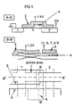
- Figure 1 shows a memory cell according to a preferred embodiment of the invention.
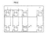
- Figure 2 shows an array of memory cells according to a preferred embodiment of the invention.
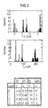
- Figure 3 shows the threshold voltages and read-out currents of cells programmed acoording to the Voltage Variant Source Side Injection methid of the present invention.
- Figure 4 shows the programming characteristics of Voltage Variant Source Side Injection.
- Figure 5 shows a state of the art Read-out architecture.
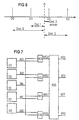
- Figure 6 shows the working principle of the Read-out architecture according to a preferred embodiment of the invention.
- Figure 7 shows the block diagram of the Read-out architecture according to a preferred embodiment of the invention.
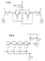
- Figure 8 shows a schematic drawing of subcircuit 400, 401, 402 and 403 of figure 7.
- Figure 9 shows a schematic drawing of subcircuit 500 of figure 7.
- Figure 10 shows the detailed layout of the Read-out architecture according to a preferred embodiment of the invention.
- Figure 11 shows experimental results representative for subcircuit 400, 401, 402 and 403.
- Figure 12 shows experimental results of the Read-out architecture according to a preferred embodiment of the invention.
- the cells can be programmed according to a method including a single charge level injection mechanism in said cells.
- the method does not require a program verify scheme, permits increased speed during programming, and reduces the area necessary for storing one bit of information.
- the speed of the programming mechanism is at least two orders of magnitude faster than other multi-level programming mechanisms described in the prior art .
- the memory device of the present invention further includes information write means, information erase means and information read-out means.
- FIG. 1 shows a memory cell of the memory device according to a preferred embodiment of the invention.
- the memory cell is a flash EEPROM cell structure implemented in a silicon substrate and comprises a source region 1, a drain region 2 and a channel region 3 therebetween.
- the memory cell further comprises a floating gate 4, said floating gate including first and second floating gate portions, said first portion extending over said channel region 3 with a thin oxide layer therebetween, said second portion extending away from said channel region.
- Said memory cell further includes a program gate 6 and a control gate 5, said program gate 6 forming a capacitor with said second floating gate portion, the control gate extending over said first portion of the floating gate.
- the program gate 6 forms a capacitor with the floating gate 4 with a high coupling ratio of about 50 % or more.
- a dielectric layer is inbetween said program gate and said floating gate and inbetween said control gate and said floating gate.
- This memory cell can be implemented in a 3 ⁇ m, or in a 1.2 ⁇ m, or in a 0.7 ⁇ m, or in a 0.5 ⁇ m, or in a 0.35 ⁇ m or in a 0.25 ⁇ m or in a 0.18 ⁇ m or in a 0.12 ⁇ m Complementary Metal-Oxide-Semiconductor (CMOS) silicon technology, or in any other CMOS technology with the set of layout rules and characteristic dimensions of the transistors according to the art.
- CMOS Complementary Metal-Oxide-Semiconductor
- the memory cell according to the preferred embodiment of the present invention when implemented in a 0.7 ⁇ m CMOS technology can have the floating gate 4, the program gate 6 and the control gate 5 being made of polysilicon material.
- the dielecric layer can be an oxide layer with a thickness of 25-30 nm.
- the thin oxide layer can have a thickness ranging from 7-9 nm.
- the floating gate length and the control gate length can be 0.7 ⁇ m, the width of the memory cell can be 1.8 ⁇ m.
- the memory device by preference comprises an array of cells as detailed hereabove.
- Figure 2 illustrates an array 11 configured in accordance with one embodiment of the present invention.
- the array is a geometric configuration of individually addressable EEPROM cells 10 as disclosed hereabove.
- the memory cells have a Control Gate 5, a Program Gate 6, a Drain region 2 and a Source region 1.
- the source 1 of all cells in the array is grounded and therefore not shown in Figure 2.
- the memory array 11 is arranged in m rows and z columns. Each cell belongs to one column and to one row only. The last four cells of each row are dummy cells which are used as references during the read-out operation of the memory device.
- a word line is connected to all the Control Gates 5 of the cells in the row.
- an output bitline is connected to all the Drains 2 of the cells.
- An input bitline is connected to all the Program Gates 6 of the cells in the column.
- the Program Gate 6 is routed in the same direction as the Drain region 2.
- the Control Gate 5 is routed in a direction perpendicular determined by the one of the Program Gate and the Drain.
- the Program Gates have to be routed by preference in parallel to the Drain regions in a Multilevel Array. In a Binary Array on the other hand, the program gates have to be routed horizontally.
- VVSSI Voltage Variant Source Side Injection
- a method of storing one of a plurality of charge levels in said memory cell is disclosed.
- a difference between the memory cells for multi-level charge storage reported in the prior art and the memory cell structure according to the preferred embodiment of the invention is that the prior art memory cells require programming schemes based on either Fowler Nordheim Tunneling (FNT) or Channel Hot Electron (CHE) injection whereas the memory cell according to this preferred embodiment of the invention employs a Voltage Variant Source Side Injection Programming method (VVSSI).
- VVSSI Voltage Variant Source Side Injection Programming method
- This new programmation method is based on a Source Side Injection (SSI) programmation method of the memory cell.
- SSI Source Side Injection
- Each of the multi-level charge storage levels corresponds to a specific threshold voltage that is stored into the Floating Gate 4 of the EEPROM memory cell.
- the threshold voltage of the memory cell is defined as the voltage that must be applied on the program gate 6 in order to obtain a drain current of 1 ⁇ A at a fixed value of the control gate voltage and the drain region voltage. This definition is different from other non-volatile memory cells for which the threshold voltage of the device must be defined at the control gate.
- the SSI programmation method devolves on applying a high voltage to said program gate 6, thereby capacitively coupling a high voltage to said floating gate 4, applying a low voltage to said control gate 5 and applying a voltage not greater than 5 Volt to said drain region whereby causing a very high hot-electron injection towards said floating gate 4 while achieving a programming of said memory cell.
- WSSI multi-level charge level programming comprises the steps of applying a single programming pulse (V PG ) to the program gate 6 of the cell, while the drain region 2 and control gates 4 are kept at a constant bias (V D and V CG ) according to the conditions of Table 1.
- the programming pulse which is applied to the program gate 6 of the memory cell has a width T of about 1 microsecond independently of the charge level to be programmed, and an amplitude which, on the contrary, is related to the charge level to be programmed as shown in Table 1.
- the amplitude of the programming pulse is given in Volt (V)
- VD (namely 5V) is the value of the power supply voltage of the 0.7 ⁇ m CMOS technology.
- the values of the different voltages reported in Table 1 can change as follows.
- V D would scale down as the power supply voltage
- the different V PG voltages would scale down as a subtraction that is approximately equal to the double of the amount by which the power supply voltage is diminished
- V CG would be in the range of 0.5-1.3 Volts.
- V CG for a 0.7 ⁇ m CMOS technology can be in the range of 1.5 to 1 Volt either or even lower.
- V D would be 3.3 Volts
- V PG would be about 9 Volt, 6, Volt, 5 Volt and 0 Volt for the different charge storage levels.
- the V PG voltages as reported in table 1 can also be different.
- a set of programming voltages as 10 Volt, 8 Volt, 6 Volt and 0 Volt for the different charge storage levels can be used.
- the set of programming voltages as given in table 1 are a good compromise between the requirements of programming speed on one hand, and accuracy of the programmed charge level on the other .
- V PG pulse width of the programming pulse
- V PG pulse width of the programming pulse
- the programming characteristic of a memory cell is defined as the shift of the threshold voltage of the memory cell versus the prgramming time.
- the time width of the pulse is concerned, it can remain about the same with the scaling down of the CMOS technology and power supply. This is certainly an advantage, because next generation VVSSI based EEPROM memory devices would be smaller in area but not slower than the embodiment in a 0.7 ⁇ m CMOS technology.
- the a method of storing one of a plurality of charge levels in said memory cell utilizes a single 1 micro second programming pulse and does not require a program verify scheme to verify the accuracy of the programmed charge storage levels.
- the speed of said programming mechanism is at least two orders of magnitude faster than other multi-level programming mechanisms based on FNT described in the prior art as for instance in M. Ohkawa et al. "A 98mm 2 64Mb Flash Memory with FN-NOR type 4-level Cell", ISSCC 96, TP 2.3, pg.36.
- a much larger current window is the main advantage of VVSSI with respect to CHE.
- An advantage of programming pulses of equal time width but different amplitudes is that the width of the pulse can be chosen in such a way that all the levels are located in the same region of the respective programming characteristics.
- 1 microsecond is the minimum time required for all the levels to end up in the saturation region of the transient characteristic as can be understood from Figure 4 .
- the memory cell by preference is erased beforehand.
- Level 0 as mentioned in table 1, in fact, is the erased state of the EEPROM memory cell according to the preferred embodiment of the present invention.
- the VVSSI programming pulses corresponding to logic levels 1, 2, and 3 according to Table 1 shift the threshold voltage of the floating gate of the memory cell by injecting into the floating gate an amount of charges which is proportional to the amplitude of the programming pulse, on the other hand the programming pulse corresponding to logic level 0 does not shift said threshold voltage since the amplitude of such pulse is zero.
- the prior art multilevel memory devices rely on a parallel architecture for reading out the information stored in the memeory cell similar to the one shown in Fig 5.
- the memory cell read out current I C is compared in parallel with three reference currents, which are chosen as the average of the currents corresponding to two adjacent logic levels.
- Each comparator 37 produces a binary output that is fed to a decoder 38 from which the 2 bits of information are obtained. Due to the considerable area cost of the comparators 37, this architecture extensively increases the periphery of the memory device. In fact, while the comparator utilized to distinguish between 0's and 1's is simple and small (1 bit resolution) in binary memories, the comparators in MLCS memory devices need to be much more accurate (8 bits resolution) and, therefore, consume much more area.
- this architecture is based on the assumption that regardless of wafer distributions of the read out current, process variations, disturbs and cycling, the read out current corresponding to level 'i' will always be larger than reference 'i' and smaller than reference 'i-1'. When this not the case, a comparator would switch, leading to an error in identifying the stored charge level. Such assumption can be made only if programming is achieved utilizing program verify techniques. Since the VVSSI programmation method is fitted of not utilizing program verification, a new custom designed architecture has been developed.
- dummy cells D0, D1, D2 and D3 are provided on each row of the memory array described above. These dummy cells are programmed to level 0,1, 2 and 3 respectively, as explained in Table 1, and are utilized as references during the read-out operation.
- the distance between the read-out current and each of the currents of the dummy cells is measured by the four subcircuits 400, 401, 402 and 403 of Fig. 7.
- Each of these produce an intermediate output voltage that is proportional to the similarity of the measured currents: this intermediate output voltage is labeled as the Matching-Score signal (MS).
- MS Matching-Score signal
- the four MS's are fed to the second stage 500 of the circuit of Fig. 7.
- This sub-block (500) decides which of the four MS's is the highest and brings the corresponding output terminal (600, 601, 602 or 603) to the high digital state, while the other three outputs remain at the low digital state.
- the high digital state corresponds to a voltage equal to the power supply voltage, while the low digital state corresonds to ground.
- the subcircuit 400 is described herebelow.
- the other subcircuits 401, 402 and 403 are similar to 400.
- the subcircuits 400, 401, 402 and 403 receive two current input signals I c and I x and deliver an intermediate voltage output signal V MS that is proportional to the similarity between the two input currents, that is in this preferred embodiment of the invention the smaller the Euclidean distance between the currents, the higher V MS .
- Fig. 8 which includes two driving n-MOS device 43, 44 comprising a couple of first driving metal-oxide-semiconductor transistors with the respective source followers 45, 42 comprising a couple of second metal-oxide-semiconductor transistors, a diode connected p-MOS device 47 comprising a third metal-oxide-semiconductor transistor and two current-to-voltage converter n-MOS device 46, 41.
- One electrode, i. e. source or drain, of each of said second metal-oxide-semiconductor transistors is connected to one electrode, i. e. source or drain, of one of said first driving metal-oxide-semiconductor transistors.
- one of said first driving metal-oxide-semiconductor transistors is connected to one of said second metal-oxide-semiconductor transistors.
- the gates of said first driving metal-oxide-semiconductor transistors and said second metal-oxide-semiconductor transistors thereby are configured in a cross-like configuration.
- each of said first driving metal-oxide-semiconductor transistors is connected to the gate of one of said second metal-oxide-semiconductor transistors, the second metal-oxide-semiconductor transistor being the one that is not connected with one electrode of said first driving metal-oxide-semiconductor transistor.
- the third metal-oxide-semiconductor transistor is connected to another electrode, i. e. source or drain, of said first driving metal-oxide-semiconductor transistors, said another electrodes of said first driving metal-oxide-semiconductor transistors being connected.
- the dimensions of the transistors are given in the figure as well. 42 and 45 have an aspect ratio W/L which can be from about 5 to about 50 times that of 43 and 44 since these are source follower transistors utilized to bias the source of the driving transistors. However, the wider the source followers with respect to the driving transistor, the more accurately the source follows the gate. Simulations show that a factor of 10 is a good compromise between accuracy and area consumption.
- the transistors 46 and 41 convert I c and I x into V C and V D respectively. If Ic is larger than I x , then 44 is cut off since the voltage at its source V C is higher than the voltage V D at its gate. However, 43 is on and the larger the difference between V C and V D , the larger its drain current, the smaller V MS . On the contrary, if I c is smaller than I x then 43 is cut off and 44 is on.
- Fig. 9 shows the proposed sub-circuit 500 according to a preferred embodiment of the invention which comprises 4 current n-MOS conveyors 50, 51, 52 and 53 comprising transistors and 4 current comparators 56, 57, 58 and 59.
- the sub-circuit receives the four V MS 's from the dummy cells D0, D1, D2, D3 as input signals at the gates of the current conveyors and delivers four binary output signals.
- the current conveyors have the source node X in common and are biased by the same biasing current I B .
- the biasing current will flow only through the conveyor with the largest V MS .
- the drain of each of the conveyors is connected to the drain of transistor 54 of the current comparator which is on top of the conveyor.
- the current comparator that is implemented according to principles known in the art, compares the current coming from the conveyor with the bias current I B /2. If the current coming from the conveyor is larger than I B /2, then the output of the comparator will be high. If, on the contrary, the current coming from the conveyor is smaller than the bias current I B /2, then the output of the comparator will be low. Since the current I B flows almost entirely in one and only one of the conveyors, it follows that one and only one of the current comparators will set its output to the high digital state, while the other three current comparators will set their output to the low digital state.
- the circuit has been integrated in a standard double-polysilicon double-metal 0.7- ⁇ m process with a silicon area of only 140 x 100 ⁇ m 2 , as shown in the picture of Fig. 10, and has been extensively evaluated.
- the silicon area for implementing a single 8-bit comparator is estimated to be around 70 x 50 ⁇ m 2 . Since 3 comparators are needed, the classical architecture of Fig. 5 would take at least 210 x 150 ⁇ m 2 of silicon area and would result in a 'level identifying' block almost 2.3 times larger than the one proposed according to this invention. For power consumption in the same range, they show comparable propagation delay. However, in the circuit proposed here it is possible to significantly decrease the propagation delay simply by increasing the circuit biasing currents.
- Fig. 11 shows the experimentally evaluated V MS as a function of a sweeping cell current in the case of a reference current of 25 ⁇ A; as expected, the better the current match, the higher V MS .
- Fig. 12 shows the experimental output voltages of the read-out circuit as a function of a sweeping cell current in the case of reference currents of 30, 80, 120 and 160 ⁇ A. Only one output voltage is high for any given cell current value.
- the dummy cells belonging to that particular sector are erased as well and reprogrammed to the reference levels. This technique ensures that both the dummy and the memory cells experience the very same duty cycle and, therefore, the same current shifts. This means that the overall shift due to cycling cancels out when comparing dummies and memory cells during read-out.
- Repeating the dummy cells on each wordline eliminates another effect that plays an important role in high density memories: the drain resistance effect. Due to the resistive nature of the drain line there is a difference in the read-out currents of the cells belonging to the same column.
Landscapes
- Engineering & Computer Science (AREA)
- Computer Hardware Design (AREA)
- Read Only Memory (AREA)
- Semiconductor Memories (AREA)
- Non-Volatile Memory (AREA)
Claims (18)
- Dispositif de mémoire adapté pour le stockage de charges multiniveaux comprenant :
une pluralité de cellules de mémoire eeprom flash comprenant une zone de source (1), une zone de drain (2), une zone de canal (3), une grille de commande (5), une grille flottante (4), et des moyens de lecture pour délivrer en parallèle des données binaires correspondant auxdits niveaux de charge stockés dans lesdites cellules; caractérisé en ce que ladite grille flottante (4) comprend des première et deuxième parties de grille flottante, ladite première partie s'étendant sur ladite zone de canal (3), ladite deuxième partie s'écartant de ladite zone de canal (3), lesdites cellules de mémoire comprennent en outre une grille de programme (6), ladite grille de programme (6) formant un condensateur avec ladite deuxième partie de grille flottante; et des moyens pour appliquer une basse tension à ladite grille de commande (5); pour appliquer à ladite zone de drain (2) une tension non supérieure à 5 volts et pour appliquer à ladite grille de programme (6) une impulsion à haute tension ayant une amplitude prédéterminée, sélectionnée d'une pluralité d'amplitudes prédéterminées et ayant une largeur essentiellement fixe, lesdites amplitudes prédéterminées déterminant lesdits niveaux de charge. - Dispositif de mémoire selon la revendication 1, dans lequel ladite pluralité de cellules de mémoire est disposée dans une matrice avec des rangées et des colonnes ayant :les drains (2) des cellules appartenant à la même colonne connectés entre eux formant ainsi une ligne de sorties de données;les grilles de programme (6) des cellules appartenant à la même colonne connectées entre elles formant ainsi une ligne d'entrées de données; etles grilles de commande (5) des cellules appartenant à la même rangée connectées entre elles formant ainsi une ligne de mots.
- Dispositif de mémoire selon la revendication 2, dans lequel ladite ligne d'entrées de données et ladite ligne de sorties de données sont essentiellement parallèles et acheminées dans la même direction; et ladite ligne de mots est acheminée dans une direction qui est essentiellement perpendiculaire à la direction de ladite ligne d'entrées de données et de ladite ligne de sorties de données.
- Dispositif de mémoire selon la revendication 3, dans lequel ladite matrice comprend en outre des cellules fictives (D0, D1, D2, D3) sur essentiellement chaque rangée de la matrice, lesdites cellules fictives (D0, D1, D2, D3) fournissant des courants de référence lors de l'opération de lecture.
- Procédé de stockage d'un d'une pluralité de niveaux de charge dans une cellule de mémoire d'un dispositif de mémoire adapté pour le stockage de charges multiniveaux, ladite cellule de mémoire comprenant une zone de source (1), une zone de drain (2), une zone de canal (3), une grille de commande (5), une grille flottante (4), caractérisé en ce que ladite grille flottante (4) comprend des première et deuxième parties de grille flottante, ladite première partie s'étendant sur ladite zone de canal (3), ladite deuxième partie s'écartant de ladite zone de canal (3), ladite cellule de mémoire comprend en outre une grille de programme (6), ladite grille de programme (6) formant un condensateur avec ladite deuxième partie de grille flottante, ledit procédé comprend les étapes consistant à:appliquer une basse tension à ladite grille de commande (5);appliquer une tension non supérieure à 5 volts à ladite zone de drain (2); etappliquer une impulsion à haute tension ayant une amplitude prédéterminée, sélectionnée d'une pluralité d'amplitudes prédéterminées et ayant une largeur essentiellement fixe, à ladite grille de programme (6), lesdites amplitudes prédéterminées déterminant lesdits niveaux de charge.
- Procédé selon la revendication 5, comprenant en outre l'étape consistant à effacer ladite cellule.
- Procédé selon la revendication 6, dans lequel essentiellement chaque cellule de mémoire dudit composant est effacée, et dans lequel ladite étape d'effacement desdites cellules de mémoire comprend les étapes consistant à:appliquer une basse tension auxdites grilles de commande (5) d'essentiellement chacune desdites cellules de ladite matrice;appliquer une tension non supérieure à 5 volts sur lesdites zones de drain (2) d'essentiellement chacune desdites cellules de ladite matrice; etappliquer une impulsion à haute tension ayant une amplitude prédéterminée et une largeur essentiellement fixe sur lesdites grilles de programme (6) d'essentiellement chacune desdites cellules de ladite matrice;et d'exécuter ensuite les étapes comme décrit dans la revendication 6.
- Procédé selon la revendication 5, dans lequel ladite impulsion à haute tension est capacitivement couplée à ladite deuxième partie de grille flottante, causant ainsi une injection d'électrons chauds vers ladite grille flottante (4), en conséquence de quoi le niveau de charge est stocké dans ladite cellule de mémoire
- Procédé selon la revendication 8, dans lequel ladite cellule de mémoire est implantée dans une technologie CMOS de 0,7 µm, ladite basse tension est inférieure ou égale à 1,5 volts et ladite impulsion à haute tension étant sélectionnée parmi les amplitudes prédéterminées de 12 volts, 8 volts, ou 7 volts, et 0 volt, ladite largeur étant d'environ 1 microseconde.
- Procédé de lecture du niveau de charge d'une cellule de mémoire d'un dispositif de mémoire, ladite cellule comprenant une cellule ayant une zone de source (1), une zone de drain (12), une zone de canal (3), une grille de commande (5) et une grille flottante (4), caractérisé en ce que ladite grille flottante (4) comprend des première et deuxième parties de grille flottante, ladite première partie s'étendant sur ladite zone de canal (3), ladite deuxième partie s'écartant de ladite zone de canal (3), ladite cellule de mémoire comprend en outre une grille de programme (6), ladite grille de programme (6) formant un condensateur avec ladite deuxième partie de grille flottante, ledit procédé comprenant les étapes consistant à:détecter le courant de drain de ladite cellule de mémoire;détecter les courants de drain d'une pluralité de cellules fictives (D0, D1, D2, D3);mesurer les similitudes entre ledit courant de drain de ladite cellule de mémoire et lesdits courants de drain de ladite pluralité de cellules fictives (D0, D1, D2, D3), en conséquence de quoi on obtient une pluralité de tensions intermédiaires représentant lesdites similitudes;déterminer la tension la plus haute parmi lesdites tensions intermédiaires, en conséquence de quoi on identifie la cellule fictive (D2) ayant le courant de drain le plus proche du courant de drain de ladite cellule de mémoire;déterminer une tension prédéterminée sur une parmi une pluralité de bornes de sortie (600, 601, 602, 603), ladite borne de sortie correspondant à ladite cellule fictive (D2) ayant le courant de drain le plus proche du courant de drain de ladite cellule de mémoire.
- Appareil pour lire le niveau de charge d'une cellule de mémoire d'un dispositif de mémoire, ladite cellule de mémoire comprenant une zone de source (1), une zone de drain (2), une zone de canal (3), une grille de commande (5) et une grille flottante (4), caractérisé en ce que ladite grille flottante (4) comprend des première et deuxième parties de grille flottante, ladite première partie s'étendant sur ladite zone de canal (3), ladite deuxième partie s'écartant de ladite zone de canal (3), ladite cellule de mémoire comprend en outre une grille de programme (6), ladite grille de programme (6) formant un condensateur avec ladite deuxième partie de grille flottante, l'appareil comprenant :une pluralité de cellules fictives (D0, D1, D2, D3) pour délivrer une pluralité de courants de référence;des moyens pour lire lesdits courants de référence et le courant de ladite cellule de mémoire;une pluralité de circuits analogiques pour mesurer la similitude entre ledit courant de ladite cellule de mémoire et chacun desdits courants de référence afin de délivrer une pluralité de tensions intermédiaires représentant lesdites similitudes;un circuit de décision pour déterminer la tension la plus haute parmi lesdites tensions intermédiaires afin de déterminer la cellule fictive (D2) ayant le courant de drain le plus proche du courant de drain de ladite cellule de mémoire; et pour déterminer une tension prédéterminée sur une parmi une pluralité de bornes de sortie (600, 601, 602, 603), ladite borne de sortie (600, 601, 602, 603) correspondant à ladite cellule fictive (D2) ayant le courant de drain le plus proche du courant de drain de ladite cellule de mémoire.
- Appareil selon la revendication 11, dans lequel ladite similitude est mesurée comme la distance euclidienne entre ledit courant de ladite cellule de mémoire et chacun desdits courants de référence.
- Appareil selon la revendication 12, dans lequel lesdits circuits analogiques comprennent un transistor à semi-conducteurs en oxyde métallique à canal long.
- Appareil selon la revendication 12, dans lequel lesdits circuits analogiques comprennent :une paire de premiers transistors de commande à semi-conducteurs en oxyde métallique (43, 44);une paire de deuxièmes transistors de commande à semi-conducteurs en oxyde métallique (42, 45), une électrode de chacun desdits deuxièmes transistors à semi-conducteurs en oxyde métallique (42, 45) étant connectée à une électrode d'un desdits premiers transistors de commande à semi-conducteurs en oxyde métallique (43, 44), un desdits premiers transistors de commande à semi-conducteurs en oxyde métallique (43, 44) étant alors connecté à un desdits deuxièmes transistors à semi-conducteurs en oxyde métallique (42, 45), la grille de chacun desdits premiers transistors de commande à semi-conducteurs en oxyde métallique (43, 44) étant connectée à la grille d'un desdits deuxièmes transistors à semi-conducteurs en oxyde métallique (42, 45), le deuxième transistor à semi-conducteurs en oxyde métallique (42, 45) étant celui qui n'est pas connecté à une électrode dudit premier transistor de commande à semi-conducteurs en oxyde métallique (43, 44), les grilles desdits premiers transistors de commande à semi-conducteurs en oxyde métallique (43, 44) et desdits deuxièmes transistors à semi-conducteurs en oxyde métallique (42, 45) étant alors configurées dans une configuration croisée; et un troisième transistor à semi-conducteurs en oxyde métallique (47) étant connecté à une autre électrode desdits premiers transistors de commande à semi-conducteurs en oxyde métallique (43, 44), lesdites autres électrodes desdits premiers transistors de commande à semi-conducteurs en oxyde métallique (43, 44) étant connectées.
- Appareil selon la revendication 14, dans lequel la grille dudit troisième transistor à semi-conducteurs en oxyde métallique (47) est en court-circuit avec l'électrode dudit troisième transistor à semi-conducteurs en oxyde métallique (47) qui est connectée auxdits premiers transistors à semi-conducteurs en oxyde métallique (43, 44).
- Appareil selon la revendication 15, dans lequel lesdits premiers transistors de commande à semi-conducteurs en oxyde métallique (43, 44) sont des transistor n-MOS, ladite électrode étant la source desdits premiers transistors de commande à semi-conducteurs en oxyde métallique (43, 44), et ladite autre électrode desdits premiers transistors de commande à semi-conducteurs en oxyde métallique (43, 44) étant le drain desdits premiers transistors de commande à semi-conducteurs en oxyde métallique (43, 44), ledit troisième transistor à semi-conducteurs en oxyde métallique (47) étant un transistor p-MOS.
- Appareil selon la revendication 14, dans lequel lesdits deuxièmes transistors à semi-conducteurs en oxyde métallique (42, 45) ont un rapport largeur/longueur qui est d'environ 10 fois le rapport largeur/longueur desdits premiers transistors à semi-conducteurs en oxyde métallique (43, 44).
- Appareil selon la revendication 11, dans lequel ledit circuit de décision comprend une pluralité de transistors de transfert de courant (50, 51, 52, 53) et de comparateurs de courant (56, 57, 58, 59), lesdits transistors de transfert de courant (50, 51, 52, 53) ayant une électrode étant connectée à la même source de polarisation de courant (X), l'électrode de grille desdits transistors de transfert de courant (50, 51, 52, 53) étant modulée par lesdites tensions intermédiaires.
Applications Claiming Priority (5)
| Application Number | Priority Date | Filing Date | Title |
|---|---|---|---|
| US1981296P | 1996-06-14 | 1996-06-14 | |
| US19812P | 1996-06-14 | ||
| US2003796P | 1996-06-21 | 1996-06-21 | |
| US20037P | 1996-06-21 | ||
| PCT/EP1997/000561 WO1997048099A1 (fr) | 1996-06-14 | 1997-02-07 | Dispositif et procede de stockage/de charge multiniveaux et de lecture |
Publications (2)
| Publication Number | Publication Date |
|---|---|
| EP0904588A1 EP0904588A1 (fr) | 1999-03-31 |
| EP0904588B1 true EP0904588B1 (fr) | 2001-07-25 |
Family
ID=26692634
Family Applications (1)
| Application Number | Title | Priority Date | Filing Date |
|---|---|---|---|
| EP97902350A Expired - Lifetime EP0904588B1 (fr) | 1996-06-14 | 1997-02-07 | Dispositif et procede de stockage/de charge multiniveaux et de lecture |
Country Status (5)
| Country | Link |
|---|---|
| US (1) | US6115285A (fr) |
| EP (1) | EP0904588B1 (fr) |
| JP (1) | JP2001508910A (fr) |
| DE (1) | DE69705837T2 (fr) |
| WO (1) | WO1997048099A1 (fr) |
Families Citing this family (28)
| Publication number | Priority date | Publication date | Assignee | Title |
|---|---|---|---|---|
| US6222762B1 (en) * | 1992-01-14 | 2001-04-24 | Sandisk Corporation | Multi-state memory |
| DE69927967T2 (de) | 1999-08-03 | 2006-07-27 | Stmicroelectronics S.R.L., Agrate Brianza | Programmierungverfahren eines nichtflüchtigen Multibit Speichers durch Regelung der Gatespannung |
| KR100387267B1 (ko) * | 1999-12-22 | 2003-06-11 | 주식회사 하이닉스반도체 | 멀티 레벨 플래쉬 이이피롬 셀 및 그 제조 방법 |
| US7057935B2 (en) * | 2001-08-30 | 2006-06-06 | Micron Technology, Inc. | Erase verify for non-volatile memory |
| US6639852B2 (en) * | 2002-01-07 | 2003-10-28 | Faraday Technology Corp. | Sensing apparatus for a ROM memory device |
| TWI244165B (en) * | 2002-10-07 | 2005-11-21 | Infineon Technologies Ag | Single bit nonvolatile memory cell and methods for programming and erasing thereof |
| TW578271B (en) * | 2002-12-18 | 2004-03-01 | Ememory Technology Inc | Fabrication method for flash memory having single poly and two same channel type transistors |
| US6956768B2 (en) * | 2003-04-15 | 2005-10-18 | Advanced Micro Devices, Inc. | Method of programming dual cell memory device to store multiple data states per cell |
| JP2005222625A (ja) * | 2004-02-06 | 2005-08-18 | Sharp Corp | 不揮発性半導体記憶装置 |
| US20060134862A1 (en) * | 2004-12-17 | 2006-06-22 | Patrice Parris | CMOS NVM bitcell and integrated circuit |
| TWI297983B (en) * | 2005-09-16 | 2008-06-11 | Novatek Microelectronics Corp | Digital-to-analog conversion device |
| US7515474B2 (en) * | 2005-09-30 | 2009-04-07 | Intel Corporation | Step voltage generator |
| US8725929B1 (en) | 2006-11-06 | 2014-05-13 | Marvell World Trade Ltd. | Adaptive read and write systems and methods for memory cells |
| US8645793B2 (en) | 2008-06-03 | 2014-02-04 | Marvell International Ltd. | Statistical tracking for flash memory |
| WO2008007174A1 (fr) * | 2006-07-10 | 2008-01-17 | Freescale Semiconductor, Inc. | Circuit de mémoire doté d'un amplificateur de sens |
| US7941590B2 (en) * | 2006-11-06 | 2011-05-10 | Marvell World Trade Ltd. | Adaptive read and write systems and methods for memory cells |
| WO2008086232A1 (fr) * | 2007-01-05 | 2008-07-17 | The Texas A & M University System | Stockage d'informations dans une mémoire |
| US7808834B1 (en) | 2007-04-13 | 2010-10-05 | Marvell International Ltd. | Incremental memory refresh |
| US8031526B1 (en) | 2007-08-23 | 2011-10-04 | Marvell International Ltd. | Write pre-compensation for nonvolatile memory |
| US8189381B1 (en) | 2007-08-28 | 2012-05-29 | Marvell International Ltd. | System and method for reading flash memory cells |
| US8085605B2 (en) | 2007-08-29 | 2011-12-27 | Marvell World Trade Ltd. | Sequence detection for flash memory with inter-cell interference |
| US8832408B2 (en) * | 2007-10-30 | 2014-09-09 | Spansion Llc | Non-volatile memory array partitioning architecture and method to utilize single level cells and multi-level cells within the same memory |
| US8441848B2 (en) | 2011-06-08 | 2013-05-14 | Micron Technology, Inc. | Set pulse for phase change memory programming |
| US8787095B2 (en) | 2012-02-28 | 2014-07-22 | Micron Technology, Inc. | Systems, and devices, and methods for programming a resistive memory cell |
| KR20140117893A (ko) * | 2013-03-27 | 2014-10-08 | 인텔렉추얼디스커버리 주식회사 | 상변화 메모리 소자 및 상변화 메모리 소자의 멀티 레벨 프로그램 방법 |
| CN111199767B (zh) * | 2018-11-16 | 2022-08-16 | 力旺电子股份有限公司 | 非易失性存储器良率提升的设计及测试方法 |
| TWI708253B (zh) * | 2018-11-16 | 2020-10-21 | 力旺電子股份有限公司 | 非揮發性記憶體良率提升的設計暨測試方法 |
| JP2020149759A (ja) * | 2019-03-15 | 2020-09-17 | キオクシア株式会社 | 半導体記憶装置 |
Family Cites Families (21)
| Publication number | Priority date | Publication date | Assignee | Title |
|---|---|---|---|---|
| CH631287A5 (fr) * | 1979-03-14 | 1982-07-30 | Centre Electron Horloger | Element de memoire non-volatile, electriquement reprogrammable. |
| US4415992A (en) * | 1981-02-25 | 1983-11-15 | Motorola, Inc. | Memory system having memory cells capable of storing more than two states |
| US4558344A (en) * | 1982-01-29 | 1985-12-10 | Seeq Technology, Inc. | Electrically-programmable and electrically-erasable MOS memory device |
| US4771404A (en) * | 1984-09-05 | 1988-09-13 | Nippon Telegraph And Telephone Corporation | Memory device employing multilevel storage circuits |
| US4616245A (en) * | 1984-10-29 | 1986-10-07 | Ncr Corporation | Direct-write silicon nitride EEPROM cell |
| US4649520A (en) * | 1984-11-07 | 1987-03-10 | Waferscale Integration Inc. | Single layer polycrystalline floating gate |
| US4670675A (en) * | 1986-02-07 | 1987-06-02 | Advanced Micro Devices, Inc. | High gain sense amplifier for small current differential |
| US5043940A (en) * | 1988-06-08 | 1991-08-27 | Eliyahou Harari | Flash EEPROM memory systems having multistate storage cells |
| US5163021A (en) * | 1989-04-13 | 1992-11-10 | Sundisk Corporation | Multi-state EEprom read and write circuits and techniques |
| US5172338B1 (en) * | 1989-04-13 | 1997-07-08 | Sandisk Corp | Multi-state eeprom read and write circuits and techniques |
| KR940006094B1 (ko) * | 1989-08-17 | 1994-07-06 | 삼성전자 주식회사 | 불휘발성 반도체 기억장치 및 그 제조방법 |
| US5583810A (en) * | 1991-01-31 | 1996-12-10 | Interuniversitair Micro-Elektronica Centrum Vzw | Method for programming a semiconductor memory device |
| BE1004424A3 (nl) * | 1991-01-31 | 1992-11-17 | Imec Inter Uni Micro Electr | Transistorstruktuur voor uitwisbare en programmeerbare geheugens. |
| US5291439A (en) * | 1991-09-12 | 1994-03-01 | International Business Machines Corporation | Semiconductor memory cell and memory array with inversion layer |
| US5298808A (en) * | 1992-01-23 | 1994-03-29 | Vitesse Semiconductor Corporation | Digital logic protocol interface for different semiconductor technologies |
| WO1993025005A1 (fr) * | 1992-05-22 | 1993-12-09 | Indiana University Foundation | Circuits d'inclusion a rendement surfacique eleve pour reseaux logiques de lukasiewich a haute densite |
| US5418743A (en) * | 1992-12-07 | 1995-05-23 | Nippon Steel Corporation | Method of writing into non-volatile semiconductor memory |
| US5422845A (en) * | 1993-09-30 | 1995-06-06 | Intel Corporation | Method and device for improved programming threshold voltage distribution in electrically programmable read only memory array |
| EP0763241B1 (fr) * | 1994-06-02 | 2001-10-17 | Intel Corporation | Memoire dynamique a cellules monobit-multibit |
| RU2190260C2 (ru) * | 1994-06-02 | 2002-09-27 | Интел Корпорейшн | Считывающая схема для флэш-памяти с многоуровневыми ячейками |
| JP2937805B2 (ja) * | 1995-05-19 | 1999-08-23 | モトローラ株式会社 | 2層フローティングゲート構造のマルチビット対応セルを有する不揮発性メモリ及びそのプログラム/消去/読出方法 |
-
1997
- 1997-02-07 EP EP97902350A patent/EP0904588B1/fr not_active Expired - Lifetime
- 1997-02-07 JP JP50109298A patent/JP2001508910A/ja not_active Ceased
- 1997-02-07 WO PCT/EP1997/000561 patent/WO1997048099A1/fr not_active Ceased
- 1997-02-07 US US09/202,481 patent/US6115285A/en not_active Expired - Lifetime
- 1997-02-07 DE DE69705837T patent/DE69705837T2/de not_active Expired - Lifetime
Also Published As
| Publication number | Publication date |
|---|---|
| US6115285A (en) | 2000-09-05 |
| JP2001508910A (ja) | 2001-07-03 |
| WO1997048099A1 (fr) | 1997-12-18 |
| EP0904588A1 (fr) | 1999-03-31 |
| DE69705837T2 (de) | 2001-11-08 |
| DE69705837D1 (de) | 2001-08-30 |
Similar Documents
| Publication | Publication Date | Title |
|---|---|---|
| US6115285A (en) | Device and method for multi-level charge/storage and reading out | |
| US5696717A (en) | Nonvolatile integrated circuit memory devices having adjustable erase/program threshold voltage verification capability | |
| US5424978A (en) | Non-volatile semiconductor memory cell capable of storing more than two different data and method of using the same | |
| US6040993A (en) | Method for programming an analog/multi-level flash EEPROM | |
| US7920422B2 (en) | All-bit-line erase verify and soft program verify | |
| JP4898117B2 (ja) | ビットラインクロストークエラーが低減された不揮発性メモリおよび方法 | |
| JP4988156B2 (ja) | 隣接フィールドエラーが低減された不揮発性メモリおよび方法 | |
| KR100259972B1 (ko) | 메모리 셀당 2개 이상의 저장 상태들을 갖는 불휘발성 반도체 메모리 장치 | |
| JP4726807B2 (ja) | 非揮発性メモリの雑/ファインプログラミングのための可変電流シンキング | |
| US6212100B1 (en) | Nonvolatile memory cell and method for programming and/or verifying the same | |
| KR20080009193A (ko) | 비휘발성 메모리 및 소스 라인 바이어스 에러들용 제어게이트 보상 방법 | |
| KR20080033460A (ko) | 비휘발성 집적 메모리 디바이스 내 셀을 프로그램하기 위한시스템 및 방법 | |
| EP1386323B1 (fr) | Compactage des tensions de seuil pour des mod les de m moires semi-conducteurs non-volatiles | |
| US6584016B2 (en) | Non-volatile memory architecture and method of operation | |
| KR100501962B1 (ko) | 전기적으로프로그램가능한메모리및프로그래밍방법 | |
| US6724662B2 (en) | Method of recovering overerased bits in a memory device | |
| US7483302B2 (en) | Non-volatile memory device and method of compensating leakage reading current of a non-volatile memory array | |
| KR20000016640A (ko) | 멀티-레벨 전하저장 장치 및 방법과 이 장치의 독출 장치 및방법 | |
| KR101357068B1 (ko) | 비휘발성 메모리들에 대한 바디 효과 감지 방법 | |
| US6416556B1 (en) | Structure and method of operating an array of non-volatile memory cells with source-side programming | |
| Montanari et al. | Multi-level charge storage in source-side injection flash EEPROM | |
| Montanari et al. | Voltage variant source side injection for multilevel charge storage in flash EEPROM | |
| JPH10199267A (ja) | 不揮発性半導体記憶装置 | |
| JPH11250678A (ja) | 半導体不揮発性記憶装置 | |
| JPH11250677A (ja) | 半導体不揮発性記憶装置およびその情報消去方法 |
Legal Events
| Date | Code | Title | Description |
|---|---|---|---|
| PUAI | Public reference made under article 153(3) epc to a published international application that has entered the european phase |
Free format text: ORIGINAL CODE: 0009012 |
|
| 17P | Request for examination filed |
Effective date: 19981204 |
|
| AK | Designated contracting states |
Kind code of ref document: A1 Designated state(s): DE FR GB IT |
|
| 17Q | First examination report despatched |
Effective date: 19990906 |
|
| GRAG | Despatch of communication of intention to grant |
Free format text: ORIGINAL CODE: EPIDOS AGRA |
|
| GRAG | Despatch of communication of intention to grant |
Free format text: ORIGINAL CODE: EPIDOS AGRA |
|
| GRAH | Despatch of communication of intention to grant a patent |
Free format text: ORIGINAL CODE: EPIDOS IGRA |
|
| RAP1 | Party data changed (applicant data changed or rights of an application transferred) |
Owner name: INFINEON TECHNOLOGIES AG |
|
| GRAH | Despatch of communication of intention to grant a patent |
Free format text: ORIGINAL CODE: EPIDOS IGRA |
|
| GRAH | Despatch of communication of intention to grant a patent |
Free format text: ORIGINAL CODE: EPIDOS IGRA |
|
| GRAA | (expected) grant |
Free format text: ORIGINAL CODE: 0009210 |
|
| AK | Designated contracting states |
Kind code of ref document: B1 Designated state(s): DE FR GB IT |
|
| REF | Corresponds to: |
Ref document number: 69705837 Country of ref document: DE Date of ref document: 20010830 |
|
| ET | Fr: translation filed | ||
| REG | Reference to a national code |
Ref country code: GB Ref legal event code: IF02 |
|
| PLBE | No opposition filed within time limit |
Free format text: ORIGINAL CODE: 0009261 |
|
| STAA | Information on the status of an ep patent application or granted ep patent |
Free format text: STATUS: NO OPPOSITION FILED WITHIN TIME LIMIT |
|
| 26N | No opposition filed | ||
| PG25 | Lapsed in a contracting state [announced via postgrant information from national office to epo] |
Ref country code: IT Free format text: LAPSE BECAUSE OF NON-PAYMENT OF DUE FEES Effective date: 20050207 |
|
| PGFP | Annual fee paid to national office [announced via postgrant information from national office to epo] |
Ref country code: GB Payment date: 20070216 Year of fee payment: 11 |
|
| PGFP | Annual fee paid to national office [announced via postgrant information from national office to epo] |
Ref country code: FR Payment date: 20070212 Year of fee payment: 11 |
|
| GBPC | Gb: european patent ceased through non-payment of renewal fee |
Effective date: 20080207 |
|
| REG | Reference to a national code |
Ref country code: FR Ref legal event code: ST Effective date: 20081031 |
|
| PG25 | Lapsed in a contracting state [announced via postgrant information from national office to epo] |
Ref country code: FR Free format text: LAPSE BECAUSE OF NON-PAYMENT OF DUE FEES Effective date: 20080229 |
|
| PG25 | Lapsed in a contracting state [announced via postgrant information from national office to epo] |
Ref country code: GB Free format text: LAPSE BECAUSE OF NON-PAYMENT OF DUE FEES Effective date: 20080207 |
|
| PGFP | Annual fee paid to national office [announced via postgrant information from national office to epo] |
Ref country code: DE Payment date: 20120123 Year of fee payment: 16 |
|
| REG | Reference to a national code |
Ref country code: DE Ref legal event code: R119 Ref document number: 69705837 Country of ref document: DE Effective date: 20130903 |
|
| PG25 | Lapsed in a contracting state [announced via postgrant information from national office to epo] |
Ref country code: DE Free format text: LAPSE BECAUSE OF NON-PAYMENT OF DUE FEES Effective date: 20130903 |