EP0905610B1 - Dual port buffer - Google Patents
Dual port buffer Download PDFInfo
- Publication number
- EP0905610B1 EP0905610B1 EP98307887A EP98307887A EP0905610B1 EP 0905610 B1 EP0905610 B1 EP 0905610B1 EP 98307887 A EP98307887 A EP 98307887A EP 98307887 A EP98307887 A EP 98307887A EP 0905610 B1 EP0905610 B1 EP 0905610B1
- Authority
- EP
- European Patent Office
- Prior art keywords
- data
- signal
- dual port
- timing
- control
- Prior art date
- Legal status (The legal status is an assumption and is not a legal conclusion. Google has not performed a legal analysis and makes no representation as to the accuracy of the status listed.)
- Expired - Lifetime
Links
Images
Classifications
-
- G—PHYSICS
- G06—COMPUTING OR CALCULATING; COUNTING
- G06F—ELECTRIC DIGITAL DATA PROCESSING
- G06F5/00—Methods or arrangements for data conversion without changing the order or content of the data handled
- G06F5/06—Methods or arrangements for data conversion without changing the order or content of the data handled for changing the speed of data flow, i.e. speed regularising or timing, e.g. delay lines, FIFO buffers; over- or underrun control therefor
- G06F5/10—Methods or arrangements for data conversion without changing the order or content of the data handled for changing the speed of data flow, i.e. speed regularising or timing, e.g. delay lines, FIFO buffers; over- or underrun control therefor having a sequence of storage locations each being individually accessible for both enqueue and dequeue operations, e.g. using random access memory
Definitions
- the present invention relates to circuitry for transferring information across a clock boundary between different clock environments, and in particular such circuitry in which a dual port RAM is utilised.
- the delay before the output changes could be longer than one clock cycle depending on the clock frequencies and design of the latch. This means that the output of the latch is indeterminate, the output from successive latches in the design could also be indeterminate, and the collective state of the entire chip rapidly becomes indeterminate.
- a known technique for passing a single bit of information between clock environments is to use a special latch which is designed to minimise the effects of metastability, commonly known as a synchroniser. If the time period for an acceptable probability of propagated metastability is longer than one clock cycle, then synchronisers are joined in series such that the output of the last synchroniser has an acceptable probability of failure.
- control signals In order to minimise the number of signals which have to pass through synchronisers, only a few control signals pass through the synchronisers and the remainder of the control signals are treated as data.
- a typical control signal passing in the same direction as the data across the clock boundary may indicate that the data is stable, and a typical control signal passing in the opposite direction may indicate the data has been accepted.
- the data being passed across the clock environment boundary is stable when it is being clocked into the receiving clock environment, then it does not suffer from metastability and does not need to pass through synchronisers.
- the data must remain stable and not change from some time before the control signal indicates that the data is stable up until the control signal in the opposite direction, after it has passed through its synchroniser indicates that the data has been accepted. This means that the data must be stored and remain unchanged for many clocks cycles. If the desired data transfer rate is slower than this number of clock cycles, there is no problem. However, as is more usual, there may be new data arriving at every clock cycle.
- the width of the data bus crossing the clock boundary must be 64 bits. This 64 bits must be held in some storage so that it is stable whilst it is crossing the clock boundary. Thus the amount of storage required is: (Protocol Latency) x (bus width)
- each synchroniser is a 1-bit data storage element, so the number of synchronisers is added to give the total storage required as: 4 x (protocol Latency) x (bus width) + synchronisers.
- circuitry for transferring information from a first timing environment to a second timing environment comprising: a dual port RAM having a first port responsive to a first clock signal having a first clock speed and a second port responsive to a second clock signal having a second clock speed different from said first clock speed; a first control circuit, responsive to the first clock signal, for controlling storage of data in the dual port RAM through the first port, and for generating a control signal indicating that the data is stored in the dual port RAM; and a second control circuit, responsive to the second clock signal, for controlling retrieval of stored data through the second port of the dual port RAM, characterised by, a first synchroniser for synchronising the control signal to the second clock signal wherein the second control circuit is additionally responsive to the synchronised control signal; and a second synchroniser for synchronising a second control signal, generated by a second control circuit indicating that data has been retrieved from the dual port, to the first timing signal, wherein the first control circuit stores data in the dual port RAM
- a RAM cell is much smaller than a flip-flip cell, and thus the chip space consumed by a dual port RAM implementation is reduced over a flip-flop implementation for the same number of storage locations.
- fewer storage locations are in any event required using a dual port RAM implementation.
- the invention also provides a method of transferring information from a first timing environment to a second timing environment, comprising the steps of: storing data in a dual port RAM through a first port thereof responsive to a first timing signal; generating a control signal, responsive to the first timing signal, indicating that data is stored in the dual port RAM; synchronising the control signal to a second timing signal; retrieving data from the dual port RAM through a second port thereof responsive to the second timing signal and the synchronised control signal; generating a second control signal, responsive to the second timing signal, indicating that data has been retrieved from the dual port RAM; and synchronising the second control signal to the first timing signal, wherein data is stored in the dual port RAM in dependence on the synchronised second control signal.
- the control signal may be synchronised to the second timing signal by a plurality of synchronisers. Also, the second control signal may be synchronised to the second timing signal by a plurality of further synchronisers.
- the first and second timing signals may be first and second clock signals.
- the first and second timing signals may be derived from a common source.
- the phase relationship variance of first and second timing signals derived from the common source may be comparable or larger than the period of either timing signal.
- the first and second timing signals may be asynchronous with respect to each other.
- the first and second timing signals, asynchronous with respect to each other, may be asynchronous or isynchronous signals.
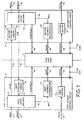
- the dual port buffer includes a dual port RAM 2, a first access control circuit 4 and a second access control circuit 6.
- the first access control circuit 4 comprises a first state machine 8, first synchronisers 10, a first address incrementer 12 and a first buffer 14.
- the second access control circuit 6 comprises second syncrhonisers 16, a second state machine 18, a second address incrementer 20 and a second buffer 22.
- the first access control circuit 4 which operates in a first timing environment under the control of a clock signal CLK1, receives from a source on bus 52 data DATA1 to be transferred to a second timing environment.
- the data DATA1 may pass through the optional first buffer 14 for the purpose of boosting the electrical drive of the signals or for re-timing under the control of the clock signal CLK1.
- the first buffer 14 outputs the data as the signals DATAIN on bus 54.
- the first buffer 14 and second buffer 22 are optional. These buffers may be present for two reasons:
- the first access control circuit 4 also receives from the source a control signal REQ1 on line 24 which the source outputs to indicate that there is valid data to be transferred to the second timing environment.
- the signal REQ1 forms an input to the first state machine 8.
- the first state machine 8 controls the transfer of the data DATA1 into the dual port RAM 2.
- the first state machine 8 outputs a signal INC1 on line 48 to the first address incrementer 12, and the first address incrementer increments the address value ADDR1 on bus 44 to the dual port RAM.
- data to be transferred is stored in successive memory locations of the dual port RAM, such that for each block of data which is stored in the dual port RAM the first address incrementer 12 increments the storage address by one block.
- the address to which the first address incrementer directs the data to be stored is an initial or base address.
- the first state machine 8 also outputs on bus 40 transmit control signals CONTROL1 to control the loading of the data into the selected address.
- CONTROL1 transmit control signals CONTROL1 to control the loading of the data into the selected address.
- the first state machine 8 outputs a signal GRANT1 on line 26 back to the source, thereby indicating to the source that the source may begin to send a further block of data on the DATA1 bus 52. Furthermore, when sufficient data has been loaded into the dual port RAM 2, the first state machine 8 sends a signal VALID on line 28 across the clock boundary to the second access control circuit 6.
- the signal VALID on line 28 is received by the second synchronisers 16 of the second access control circuit 6, and the synchronised output of the second syncrhonisers 16, being the signal VALID synchronised to the second clock signal CLK2, forms an input to the second state machine 18.
- the second state machine 18 In response to the synchronised signal VALID the second state machine 18 outputs control signals on the second control bus CONTROL2 42 to the dual port RAM 2, and outputs a signal INC2 on line 50 to the second address incrementer 20. This process is repeated according to how much data was transferred.
- the second state machine 18 controls the access of a data block stored in the dual port RAM at a location identified by the address ADDR2 on the address bus 46 output from the second address incrementer.
- the second address incrementer in its initial state, retrieves data blocks from a base address, and thereafter from successive address locations.
- the second address incrementer follows the first address incrementer such that data is first retrieved from the block to which data has first been written, and so on through successive memory access cycles.
- the data block which has been stored in the dual port RAM by the first access control circuit 4 is output as DATAOUT on the data bus 56 and stored in the second buffer 22 under the control of the clock signal CLK2 on line 62.
- the second state machine 18 sets a signal ACK on line 30 which is transferred to the first timing environment and the first access control circuit 4.
- the signal ACK is received by the first synchronisers 10, and the synchronised output thereof is input on line 32 to the first state machine 8.
- the first state machine 8 receives the synchronised signal ACK on line 32 it indicates that there is further space in the dual port RAM for the first access control circuit to load data into.
- the second state machine 18 also outputs a signal REQ2 on line 36 to a destination circuit which the data is to be transferred to in the second timing environment, when the data block has been successfully accessed from the dual port RAM 2.
- This signal indicates that valid data is available on.the data bus 58 on the output of the second buffer 22.
- the destination circuit receives the signal REQ2 it loads therein the data DATA2 on the bus 58 and once this is done returns a signal GRANT2 on line 38 to the second state machine 18, in response to which the second state machine 18 can, if further data blocks are available in the dual port RAM 2, access these data blocks and forward them to the destination circuit.
- the control protocol between the two timing environments is a single signal VALID in one direction from the first timing environment to the second timing environment, and a single signal ACK in the other direction from the second timing environment to the first timing environment.
- the particular protocol that is used to control the flow of data across the timing boundary may vary considerably according to the desired application, the volume of flow of data, and the relative speeds of the two clocks of the respective timing environment. For instance, if the clock signal CLK2 in the second timing environment was much faster than the clock signal CLK1 in the first timing environment, then it is possible that the return signal of the protocol described with reference to Figure 1, i.e. the signal ACK on line 30 could be dispensed with.
- the flow control signals according to the protocol of Figure 1 could in fact be comprised of a plurality of signals, the flow control protocol being more complex. If the flow control signals in either direction comprised a plurality of signals, then each of such signals would have synchronisers such as the synchronisers 10 and 16 associated therewith. Each of the plurality of control signals may have one or more synchronisers, in series, associated therewith.
- control signals in both directions comprise a plurality of control signals
- the number of signals in each direction may differ, for example if a different protocol is being used in each direction, or be the same.
- edges of any one of the control signals used may be active edges.
- the dual port RAM 2 could be split into two halves, and each of the signals VALID and ACK could comprise two signals, one associated with the top half of the dual port RAM 2 and the other associated with the bottom half of the dual port RAM 2.
- the dual port buffer described hereinabove transfers data or information in one direction only from a first clock environment to a second clock environment. In order to allow the transfer of data in the other direction from the second clock environment to the first clock environment it is necessary to provide a second dual port buffer.
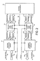
- Figure 2 there is shown such an implementation where the exemplary dual port buffer described hereinabove with reference to Figure 1 is shown duplicated for use for transmitting data to and from a system environment.
- Figure 2 illustrates the use of the dual port buffer of Figure 1, in two instances, as an interface between, firstly, on-chip functional circuitry operating in a clock environment determined by various on-chip requirements and means, and, secondly, an off-chip data source and data sink each having separate clocks determined by off-chip requirements and possibly off-chip means.
- the system environment is generally designated as 78, and there is also shown therein a receive interface driver 70, a receive dual port buffer 74, a transmit dual port buffer 76 and a transmit interface driver 72.
- Each of the receive dual port buffer 74 and transmit dual port buffer 76 are, in the preferred embodiment, identical to the dual port buffer described hereinabove with reference to Figure 1.
- the system environment 78 may include a central processor unit, a digital signal processor, or some form of specific logic circuitry.
- the receive interface driver 70 receives data RXDATA on a bus 82 and protocol control signals RXCONTROL on lines 80 from a source. Under the control of a receive clock RXCLK on line 98 the receive interface driver 70 transfers the data from the source on the bus 82 to the bus 88 as data RXDATA1. As will be understood and in line with normal flow control protocol techniques, when the data is transferred to the bus 88 then the receive interface driver 70 sends flow control signals on the signals RXCONTROL on line 80 back to the source to indicate that the data has been received.
- the data output by the receive interface driver 70 on bus 88 as RXDATA1 is output simultaneously with the signal RX on line 84 which, as discussed hereinabove with reference to Figure 1, is a protocol control signal.
- the receive dual port buffer 74 then transfers the data RXDATA1 on bus 88 from the clock environment of the clock signal RXCLK to the system clock environment on the data bus RXDATA2 on bus 94.
- the receive dual port buffer is clocked by the receive clock RXCLK and also a system clock SYSCLK on line 96.
- the data RXDATA2 on the bus 94 is synchronised to the system clock SYSLCK and received in the system environment 78.
- the system environment outputs data TXDATA1 on bus 112 under the control of the system clock SYSCLK for transmission in a different clock environment on bus TXDATA2 on bus 106.
- the data TXDATA2 on bus 106 corresponds directly to the data TXDATA1 on bus 112 but is synchronised to a transmit clock TXCLK on line 100.
- the transmit dual port buffer 76 operates in identical fashion to that described with reference to Figure 1.
- the data TXDATA2 on bus 106 is transmitted by the transmit interface driver 72 onto bus 102 as TXDATA for transmission to a destination circuit.
- the control of the TXDATA on bus 102 from the transmit interface driver 72 is controlled by protocol control signals TXCONTROL on lines 104.
- the destination circuits and source circuits may be on-chip or off-chip.
- both the receive interface driver 70 and the transmit interface driver 72 may interface with a plurality of source and destination circuits.
- the receive interface driver may include polling circuitry for determining the priority of a source attempting to send data to the system environment 78, and the protocol control signals RXCONTROL on lines 80 may include control signals for polling various sources.
- the transmit interface driver 72 may include polling circuitry for determining the destination of the data to be transmitted, and for transmitting data to the destination having highest priority.
- the receive interface driver 70 and the transmit interface driver 72 may also include interrupt circuitry, such that if data being buffered therein for either transmission to or transmission from the system environment has a higher priority in terms of the address of its source or destination than other buffered data, then the data associated with the highest priority source/destination is transmitted first.
- the system environment may comprise cell engines (in respect of which reference is made to The ATM Forum, Technical Committee. Utopia, An ATM-PHY Interface Specification, Level 2 Version 1.0 21 November 1996. AF-PHY-0039.000 Editors: Des YOUNG et al. ALANTEC, 70 Plumeria Drive, An Jose, CA 95134-2134), and may interface directly to individual devices via a plurality of receive and transmit dual port buffers.
- the dual port buffers may interface to a data-strobe serial link according to IEEE 1355, a central processor unit, or another system environment.
- the dual port buffers may also interface the system environment to a SDRAM.
- the dual port RAM is preferably fully accessible by one of the timing environments such that the dual port RAM may be tested for production purposes using a function test as opposed to a structural scan test or a built in self-test engine, which may be expensive to implement for a small dual port RAM. Any sort of structure test of the dual port RAM may be implemented.
Landscapes
- Engineering & Computer Science (AREA)
- Theoretical Computer Science (AREA)
- Physics & Mathematics (AREA)
- General Engineering & Computer Science (AREA)
- General Physics & Mathematics (AREA)
- Information Transfer Systems (AREA)
- Synchronisation In Digital Transmission Systems (AREA)
Applications Claiming Priority (2)
| Application Number | Priority Date | Filing Date | Title |
|---|---|---|---|
| GB9720811 | 1997-09-30 | ||
| GBGB9720811.0A GB9720811D0 (en) | 1997-09-30 | 1997-09-30 | Dual port buffer |
Publications (2)
| Publication Number | Publication Date |
|---|---|
| EP0905610A1 EP0905610A1 (en) | 1999-03-31 |
| EP0905610B1 true EP0905610B1 (en) | 2003-11-12 |
Family
ID=10819871
Family Applications (1)
| Application Number | Title | Priority Date | Filing Date |
|---|---|---|---|
| EP98307887A Expired - Lifetime EP0905610B1 (en) | 1997-09-30 | 1998-09-29 | Dual port buffer |
Country Status (5)
| Country | Link |
|---|---|
| US (1) | US6249875B1 (2) |
| EP (1) | EP0905610B1 (2) |
| JP (1) | JPH11175313A (2) |
| DE (1) | DE69819648T2 (2) |
| GB (1) | GB9720811D0 (2) |
Families Citing this family (22)
| Publication number | Priority date | Publication date | Assignee | Title |
|---|---|---|---|---|
| US6700872B1 (en) * | 1998-12-11 | 2004-03-02 | Cisco Technology, Inc. | Method and system for testing a utopia network element |
| KR100443014B1 (ko) * | 2001-12-24 | 2004-08-04 | 엘지전자 주식회사 | 듀얼포트램을 이용한 상이위상 클럭간 데이터 전송 장치 |
| US7194650B2 (en) * | 2003-05-09 | 2007-03-20 | Hewlett-Packard Development Company, L.P. | System and method for synchronizing multiple synchronizer controllers |
| US7245684B2 (en) * | 2003-05-09 | 2007-07-17 | Hewlett-Packard Development Company, L.P. | System and method for compensating for skew between a first clock signal and a second clock signal |
| US7219251B2 (en) * | 2003-05-09 | 2007-05-15 | Hewlett-Packard Development Company, L.P. | Programmable clock synchronizer |
| US7100065B2 (en) * | 2003-05-09 | 2006-08-29 | Hewlett-Packard Development Company, L.P. | Controller arrangement for synchronizer data transfer between a core clock domain and bus clock domain each having its own individual synchronizing controller |
| US7480357B2 (en) * | 2003-05-10 | 2009-01-20 | Hewlett-Packard Development Company, L.P. | System and method for effectuating the transfer of data blocks across a clock boundary |
| US7623482B2 (en) * | 2003-05-10 | 2009-11-24 | Hewlett-Packard Development Company, L.P. | System and method for effectuating the transfer of data blocks including a header block across a clock boundary |
| US7382847B2 (en) * | 2004-07-23 | 2008-06-03 | Hewlett-Packard Development Company, L.P. | Programmable sync pulse generator |
| US7340631B2 (en) * | 2004-07-23 | 2008-03-04 | Hewlett-Packard Development Company, L.P. | Drift-tolerant sync pulse circuit in a sync pulse generator |
| US7119582B2 (en) * | 2004-07-23 | 2006-10-10 | Hewlett-Packard Development Company, Lp. | Phase detection in a sync pulse generator |
| US20060023819A1 (en) * | 2004-07-29 | 2006-02-02 | Adkisson Richard W | Clock synchronizer |
| US7436917B2 (en) * | 2004-07-29 | 2008-10-14 | Hewlett-Packard Development Company, L.P. | Controller for clock synchronizer |
| US9138825B2 (en) * | 2005-10-07 | 2015-09-22 | Illinois Tool Works Inc. | Wireless communication system for welding-type devices |
| JP4851964B2 (ja) * | 2007-03-05 | 2012-01-11 | Necアクセステクニカ株式会社 | デュアルポートメモリを用いた同期化回路 |
| EP2320327A1 (en) * | 2009-11-09 | 2011-05-11 | Imec | A data transferring device |
| EP2360598A1 (en) * | 2010-02-12 | 2011-08-24 | Blue Wonder Communications GmbH | Method and device for synchronizing data broadcasts |
| US8826062B2 (en) | 2011-05-23 | 2014-09-02 | Intel Mobile Communications GmbH | Apparatus for synchronizing a data handover between a first clock domain and a second clock domain through phase synchronization |
| US8918666B2 (en) * | 2011-05-23 | 2014-12-23 | Intel Mobile Communications GmbH | Apparatus for synchronizing a data handover between a first and second clock domain through FIFO buffering |
| US9706508B2 (en) * | 2013-04-05 | 2017-07-11 | Honeywell International Inc. | Integrated avionics systems and methods |
| US11321511B2 (en) | 2019-07-09 | 2022-05-03 | SiFive, Inc. | Reset crossing and clock crossing interface for integrated circuit generation |
| US10902171B1 (en) * | 2019-07-09 | 2021-01-26 | SiFive, Inc. | Clock crossing interface for integrated circuit generation |
Family Cites Families (17)
| Publication number | Priority date | Publication date | Assignee | Title |
|---|---|---|---|---|
| JPS5782217A (en) * | 1980-11-10 | 1982-05-22 | Matsushita Electric Ind Co Ltd | Pcm recorder possible for synchronizing run |
| US4769792A (en) | 1986-10-28 | 1988-09-06 | Kabushiki Kaisha Toshiba | Semiconductor memory device with voltage bootstrap |
| US5146477A (en) * | 1987-03-17 | 1992-09-08 | Antonio Cantoni | Jitter control in digital communication links |
| US4805171A (en) * | 1987-07-10 | 1989-02-14 | Solid State Systems, Inc. | Unitary PCM rate converter and multiframe buffer |
| US5029124A (en) * | 1988-05-17 | 1991-07-02 | Digital Equipment Corporation | Method and apparatus for providing high speed parallel transfer of bursts of data |
| JP2536929B2 (ja) * | 1989-07-21 | 1996-09-25 | 富士通株式会社 | 位相整合回路 |
| DE4011241B4 (de) * | 1990-04-06 | 2005-06-02 | Micronas Gmbh | Digitale Fernsehsignalverarbeitungsschaltung mit orthogonalem Ausgangstakt |
| US5933580A (en) * | 1991-09-04 | 1999-08-03 | Canon Kabushiki Kaisha | Scanner printer server |
| US5379384A (en) * | 1992-06-05 | 1995-01-03 | Intel Corporation | Configuration data loopback in a bus bridge circuit |
| US5509038A (en) * | 1994-04-06 | 1996-04-16 | Hal Computer Systems, Inc. | Multi-path data synchronizer system and method |
| US5469851A (en) * | 1994-08-09 | 1995-11-28 | Hewlett-Packard Company | Time multiplexed digital ultrasound beamformer |
| JPH0876713A (ja) * | 1994-09-02 | 1996-03-22 | Komatsu Ltd | ディスプレイ制御装置 |
| KR0177731B1 (ko) * | 1994-09-15 | 1999-05-15 | 정장호 | 망동기용 디지탈 위상동기루프 제어방법 |
| US5537362A (en) | 1994-12-06 | 1996-07-16 | National Semiconductor Corporation | Low-voltage EEPROM using charge-pumped word lines |
| US5822341A (en) * | 1995-04-06 | 1998-10-13 | Advanced Hardware Architectures, Inc. | Multiport RAM for use within a viterbi decoder |
| SG77135A1 (en) * | 1996-04-26 | 2000-12-19 | Texas Instruments Inc | Method and system for assigning a channel number to a received data packet |
| US6088272A (en) * | 1997-10-24 | 2000-07-11 | Oki Data Corporation | Data output system |
-
1997
- 1997-09-30 GB GBGB9720811.0A patent/GB9720811D0/en not_active Ceased
-
1998
- 1998-09-29 DE DE69819648T patent/DE69819648T2/de not_active Expired - Fee Related
- 1998-09-29 EP EP98307887A patent/EP0905610B1/en not_active Expired - Lifetime
- 1998-09-30 US US09/164,227 patent/US6249875B1/en not_active Expired - Lifetime
- 1998-09-30 JP JP10278224A patent/JPH11175313A/ja active Pending
Also Published As
| Publication number | Publication date |
|---|---|
| EP0905610A1 (en) | 1999-03-31 |
| GB9720811D0 (en) | 1997-12-03 |
| DE69819648D1 (de) | 2003-12-18 |
| US6249875B1 (en) | 2001-06-19 |
| DE69819648T2 (de) | 2004-09-30 |
| JPH11175313A (ja) | 1999-07-02 |
Similar Documents
| Publication | Publication Date | Title |
|---|---|---|
| EP0905610B1 (en) | Dual port buffer | |
| JP3856696B2 (ja) | 2倍データ速度同期式動的ランダムアクセスメモリのための構成可能同期装置 | |
| US8352774B2 (en) | Inter-clock domain data transfer FIFO circuit | |
| US6678811B2 (en) | Memory controller with 1X/MX write capability | |
| US6633965B2 (en) | Memory controller with 1×/M× read capability | |
| US6530006B1 (en) | System and method for providing reliable transmission in a buffered memory system | |
| US8520464B2 (en) | Interface circuit and semiconductor device incorporating same | |
| US6973078B2 (en) | Method and apparatus for implementing low latency crossbar switches with integrated storage signals | |
| US5809521A (en) | Single and multistage stage fifo designs for data transfer synchronizers | |
| US20020172079A1 (en) | Memory controller receiver circuitry with tri-state noise immunity | |
| JP2004521426A (ja) | バスサイクル毎に選択可能な数のデータワードの読み出し及び/又は書き込みを行うことができるファーストイン・ファーストアウトバッファ | |
| US5758131A (en) | Bus adapter for synchronizing communications between two circuits running at different clock rates | |
| US5917761A (en) | Synchronous memory interface | |
| US8176353B2 (en) | Method for the data transfer between at least two clock domains | |
| KR100617999B1 (ko) | 메모리 장치 내의 데이터 캡처를 위한 방법 및 장치 | |
| GB2521035A (en) | A synchronous bridge circuitry and a method of transferring data using asynchronous bridge circuitry | |
| US7027542B1 (en) | Apparatus and method for providing data transfer between two digital circuits with different clock domains and for solving metastability problems | |
| US20020144171A1 (en) | Multiple clock domain de-skewing technique | |
| US6928027B2 (en) | Virtual dual-port synchronous RAM architecture | |
| US6629226B1 (en) | Fifo read interface protocol | |
| US6055588A (en) | Single stage FIFO memory with a circuit enabling memory to be read from and written to during a single cycle from a single clock | |
| US6282149B1 (en) | Circuit and method for synchronized data banking | |
| EP2515443A1 (en) | Data serializer | |
| US7328361B2 (en) | Digital bus synchronizer for generating read reset signal | |
| US12554283B2 (en) | Clock domain crossing synchronization circuits and methods to guarantee proper data signal order |
Legal Events
| Date | Code | Title | Description |
|---|---|---|---|
| PUAI | Public reference made under article 153(3) epc to a published international application that has entered the european phase |
Free format text: ORIGINAL CODE: 0009012 |
|
| AK | Designated contracting states |
Kind code of ref document: A1 Designated state(s): DE FR GB IT |
|
| AX | Request for extension of the european patent |
Free format text: AL;LT;LV;MK;RO;SI |
|
| 17P | Request for examination filed |
Effective date: 19990916 |
|
| AKX | Designation fees paid |
Free format text: DE FR GB IT |
|
| 17Q | First examination report despatched |
Effective date: 20020311 |
|
| GRAH | Despatch of communication of intention to grant a patent |
Free format text: ORIGINAL CODE: EPIDOS IGRA |
|
| GRAS | Grant fee paid |
Free format text: ORIGINAL CODE: EPIDOSNIGR3 |
|
| GRAA | (expected) grant |
Free format text: ORIGINAL CODE: 0009210 |
|
| AK | Designated contracting states |
Kind code of ref document: B1 Designated state(s): DE FR GB IT |
|
| PG25 | Lapsed in a contracting state [announced via postgrant information from national office to epo] |
Ref country code: IT Free format text: LAPSE BECAUSE OF FAILURE TO SUBMIT A TRANSLATION OF THE DESCRIPTION OR TO PAY THE FEE WITHIN THE PRE;WARNING: LAPSES OF ITALIAN PATENTS WITH EFFECTIVE DATE BEFORE 2007 MAY HAVE OCCURRED AT ANY TIME BEFORE 2007. THE CORRECT EFFECTIVE DATE MAY BE DIFFERENT FROM THE ONE RECORDED.SCRIBED TIME-LIMIT Effective date: 20031112 |
|
| REG | Reference to a national code |
Ref country code: GB Ref legal event code: FG4D |
|
| REF | Corresponds to: |
Ref document number: 69819648 Country of ref document: DE Date of ref document: 20031218 Kind code of ref document: P |
|
| ET | Fr: translation filed | ||
| PLBE | No opposition filed within time limit |
Free format text: ORIGINAL CODE: 0009261 |
|
| STAA | Information on the status of an ep patent application or granted ep patent |
Free format text: STATUS: NO OPPOSITION FILED WITHIN TIME LIMIT |
|
| 26N | No opposition filed |
Effective date: 20040813 |
|
| PGFP | Annual fee paid to national office [announced via postgrant information from national office to epo] |
Ref country code: GB Payment date: 20070925 Year of fee payment: 10 |
|
| PGFP | Annual fee paid to national office [announced via postgrant information from national office to epo] |
Ref country code: DE Payment date: 20070928 Year of fee payment: 10 |
|
| PGFP | Annual fee paid to national office [announced via postgrant information from national office to epo] |
Ref country code: FR Payment date: 20070926 Year of fee payment: 10 |
|
| GBPC | Gb: european patent ceased through non-payment of renewal fee |
Effective date: 20080929 |
|
| REG | Reference to a national code |
Ref country code: FR Ref legal event code: ST Effective date: 20090529 |
|
| PG25 | Lapsed in a contracting state [announced via postgrant information from national office to epo] |
Ref country code: DE Free format text: LAPSE BECAUSE OF NON-PAYMENT OF DUE FEES Effective date: 20090401 |
|
| PG25 | Lapsed in a contracting state [announced via postgrant information from national office to epo] |
Ref country code: FR Free format text: LAPSE BECAUSE OF NON-PAYMENT OF DUE FEES Effective date: 20080930 |
|
| PG25 | Lapsed in a contracting state [announced via postgrant information from national office to epo] |
Ref country code: GB Free format text: LAPSE BECAUSE OF NON-PAYMENT OF DUE FEES Effective date: 20080929 |