EP0905712B1 - Procédé et dispositif pour la programmation analogique d'une cellule de mémoire EEPROM flash avec autovérification - Google Patents
Procédé et dispositif pour la programmation analogique d'une cellule de mémoire EEPROM flash avec autovérification Download PDFInfo
- Publication number
- EP0905712B1 EP0905712B1 EP97830477A EP97830477A EP0905712B1 EP 0905712 B1 EP0905712 B1 EP 0905712B1 EP 97830477 A EP97830477 A EP 97830477A EP 97830477 A EP97830477 A EP 97830477A EP 0905712 B1 EP0905712 B1 EP 0905712B1
- Authority
- EP
- European Patent Office
- Prior art keywords
- terminal
- cell
- voltage
- mos transistor
- output
- Prior art date
- Legal status (The legal status is an assumption and is not a legal conclusion. Google has not performed a legal analysis and makes no representation as to the accuracy of the status listed.)
- Expired - Lifetime
Links
- 238000000034 method Methods 0.000 title claims description 12
- 239000003990 capacitor Substances 0.000 claims description 5
- 230000002596 correlated effect Effects 0.000 claims description 4
- 238000012544 monitoring process Methods 0.000 claims 1
- 239000008186 active pharmaceutical agent Substances 0.000 description 16
- 230000007423 decrease Effects 0.000 description 4
- 238000010586 diagram Methods 0.000 description 4
- 230000001419 dependent effect Effects 0.000 description 3
- 239000002784 hot electron Substances 0.000 description 3
- 238000003491 array Methods 0.000 description 2
- 230000000875 corresponding effect Effects 0.000 description 2
- 230000006870 function Effects 0.000 description 2
- 238000002347 injection Methods 0.000 description 2
- 239000007924 injection Substances 0.000 description 2
- 230000009467 reduction Effects 0.000 description 2
- 238000012795 verification Methods 0.000 description 2
- 230000004888 barrier function Effects 0.000 description 1
- 230000008859 change Effects 0.000 description 1
- 230000000694 effects Effects 0.000 description 1
- 230000005684 electric field Effects 0.000 description 1
- 230000008030 elimination Effects 0.000 description 1
- 238000003379 elimination reaction Methods 0.000 description 1
- 238000004519 manufacturing process Methods 0.000 description 1
- 230000004048 modification Effects 0.000 description 1
- 238000012986 modification Methods 0.000 description 1
- 230000003071 parasitic effect Effects 0.000 description 1
- 239000000243 solution Substances 0.000 description 1
Images

Classifications
-
- G—PHYSICS
- G11—INFORMATION STORAGE
- G11C—STATIC STORES
- G11C27/00—Electric analogue stores, e.g. for storing instantaneous values
- G11C27/005—Electric analogue stores, e.g. for storing instantaneous values with non-volatile charge storage, e.g. on floating gate or MNOS
Definitions
- the present invention relates to a method and a device for analog programming of flash EEPROM memory cells with autoverify.
- a flash memory array 1 comprises a plurality of flash cells 2 disposed on lines and columns, in which the gate terminals of the cells 2 disposed on one and the same line are connected to a respective word line 3, the drain terminals of the cells 2 disposed on one and the same column are connected to a respective bit line 4 and the source terminals are generally connected to ground.
- the word lines 3 are connected to a row decoder 5 and the bit lines 4 are connected to a column decoder 6 which receive respective address and control signals from a control unit 7 which permits the selection, from time to time, of a single word line 3 and a single bit line 4 and the biasing of the cell 2 connected to the word line and to the bit line selected at the operating voltages provided.
- a cell 2 may be read by connecting the selected word line 3 to an external voltage V G of preset value (such as 8-9 V) and forcing a biasing current I f into the selected bit line 4.
- V G preset value
- I f K*(W/L)*[(V G - V th ) - V DS /2]*V DS in which K is a constant associated with the production process, W/L is the dimensional width/length ratio of the cell, V th is the threshold voltage of the cell (or the minimum voltage to be applied between the gate and source terminals of the cell so that it begins to conduct current) and V DS is the drain/source drop of the cell.
- K*(W/L)*V DS GM f represents the transconductance (gain) of the cell and the term (V G - Vth) represents the overdrive of the cell.
- the drop V DS is constant and the term V DS /2 is negligible with respect to the overdrive (V G -V th ); consequently, in this state the current I f flowing through the cell depends linearly on the threshold voltage V th .
- the latter is selected by biasing the selected word and bit lines at respective preset programming voltage values.
- Writing takes place thanks to the phenomenon of hot electron injection, whereby the high voltage supplied to the drain terminal of the cell to be written causes an increase in the velocity of the electrons and some of them achieve sufficient energy to overcome the barrier of the oxide.
- the electric field which is created accelerates the electrons through the layer of oxide which separates the channel region from the floating gate region and permits the trapping of those electrons inside the floating gate region.
- the cell modifies its threshold voltage because of this trapping of the electrons.
- the phenomenon of hot electron injection is not controlled and not repeatable with accuracy; consequently, at the present time, during programming, the cell is read several times for reading the threshold voltage reached (verify phase).
- US-A-5 606 522 discloses an analog memory including a cell array, a comparator, a mode selector, and a controller.
- the cell array includes a plurality of memory cells each having a control gate, an injector, and a floating gate, and a first input part of a differential input stage.
- a first high-voltage pulse signal is applied to the control gate and a second high-voltage pulse signal is applied to the injector.
- Charges are injected into or are erased from the floating gate through the injector.
- the comparator has a differential input port whose first input is a reference voltage signal and whose second input is a floating gate voltage signal of one of the plurality of memory cells.
- the comparator compares and outputs the difference between the reference voltage signal and the floating gate voltage signal.
- the mode selector connects the output of the comparator to the first input, functions as a unit amplifier during a reading mode, and connects the external reference voltage signal to the first input of the comparator during a writing mode.
- the controller maintains a program enable state if the current state of the comparator output signal is the same as its previous state and maintains a program disable state if the current state is different from the previous state.
- the controller generates first and second high-voltage pulse signals according to the state of the comparator output signal.
- the object of the invention is therefore to provide a method and a device which permit the verification of the threshold reached by flash-EEPROM cells during programming.
- the present invention provides a method and a device for analog programming of flash EEPROM memory cells with autoverify, as defined in Claims 1 and 4 respectively.
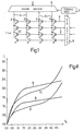
- Fig. 2 shows the programming and verify device 10 as connected to a cell to be read 2 belonging to the memory array 1 shown in Fig. 1.
- the programming and verify device 10 shows only the cell to be read 2 addressed via the row decoder 5 and the column decoder 6; the row decoder 5 has been omitted and only the essential elements of the column decoder 6 have been shown.
- the cell to be read 2 has source terminal 11 connected to ground, gate terminal 12 biased at the programming voltage V G and drain terminal 13 connected to a node 18 via a selector switch 16 and a first biasing transistor 17 of NMOS type, both belonging to the column decoder 6 of Fig. 1.
- the node 18 is connected to a current mirror device 19 formed by two PMOS transistors 21, 22; in detail, the PMOS transistor 21 is diode-connected (i.e.
- the node 24 is connected to the drain terminal 28 of a reference transistor 27, of NMOS type, having source terminal 29 connected to ground and gate terminal 30 connected to the output of an operational amplifier 31; this latter has inverting input connected to the node 18 and non-inverting input connected to the node 24.
- the second biasing transistor 25 has gate terminal connected to the gate terminal of the first biasing transistor 17 and to a biasing node 15 to which a biasing voltage V B is supplied.
- the biasing transistors 17 and 25 have the function of biasing the cell 2 and the reference transistor 27 at the desired voltage on the basis of the operating condition provided.
- Fig. 2 also shows the output voltage V o of the operational amplifier 31, also forming the output voltage of the programming and verify device 10; the voltage drop V DS,2 and V DS,27 between the drain and source terminals of the cell to be read 2 and, respectively, the reference transistor 27; as well as the currents I 2 and I 27 flowing through the cells.
- European patent application No. 97830172.9 published as EP-A-0 872 850, entitled "High-precision analog reading circuit for memory arrays, in particular analog flash memory arrays" filed on 15.4.97 in the name of the same applicant, incorporated here for reference, describes a read device structurally similar to that of Fig. 2, in which a flash cell similar to the cell 2 is provided in place of reference transistor 27.
- European application No. 97830172.9 it has been shown, as briefly reported below, that the output voltage V o of the operational amplifier 31 is linearly dependent on the threshold voltage V th,2 of the cell 2.
- I 2 K* (W/L)*[(V G - V th,2 ) - V DS,2 /2]*V DS,2
- I R K* (W/L)*[(V o - V th,R ) - V DS,R /2]*V DS,R in which V th,2 and V th,R are the threshold voltages of the cell to be read 2 and of the reference cell respectively, V DS,R is the source/drain drop of the reference cell and the other variables have the meaning already explained.
- V G - V th,2 V o - V th,R
- V o V G - (V th,2 - V th,R )
- a high voltage V B is supplied to the gate terminal of the biasing transistors 17, 25 so as to bring the drain terminal 13 of the cell to be programmed 2 to the programming drain voltage (7-8 V for example); a high voltage V G (12 V for example) is also applied to the gate terminal 12 of the cell 2.
- V G (12 V for example) is also applied to the gate terminal 12 of the cell 2.
- hot electrons are injected into the floating gate region of the cell 2 which thus gradually modifies its threshold voltage.
- the currents I 2 and I 27 are no longer equal but are nonetheless correlated and the output voltage V o is still linearly dependent on the instantaneous threshold voltage of the cell 2.
- the current I 2 flowing in the cell 2 decreases, the voltage at the node 18 increases, the output voltage V o and hence the voltage at the gate terminal of the reference transistor 27 decreases and its current I 27 decreases; in particular, the reduction of the current I 27 is substantially equal to the decrease of the current I 2 flowing in the cell 2, as can also be seen from Fig. 4 showing the plot of the currents I 2 and I 27 for the cell 2 and the transistor 27 versus the gate voltage V G for two different threshold voltage values corresponding to two different moments of programming.
- the curves A and B refer to current I 2 of cells 2 having threshold voltages V th' and V th'' , where V th' ⁇ V th'' and the curves C and D refer to the plots of current I 27 in the conditions of the curves A and B.
- the current characteristics of the cell 2 and of the reference transistor 27 move contemporaneously downwards because of the increase of the threshold voltage of the cell 2 and of the corresponding reduction of the gate voltage of the reference transistor 27.
- Fig. 3 shows a more complete embodiment of the device 10, equipped with means for automatically interrupting the programming when the desired threshold voltage is reached, and with means of compensation of the loop formed by the components 31, 27, 26, 25 and 22.
- Fig. 3 shows a comparator 36, having a first input connected to the output of the operational amplifier 31 and a second input receiving a reference voltage V TAR representing the target voltage, correlated to the threshold voltage desired for the cell 2; the output of the comparator 36 is connected to a selection input 37a of a switch 37 selectively connecting one of two nodes 37b, 37c to the biasing node 15.
- the node 37b is connected to a first voltage source 38 supplying the programming biasing voltage V H and the node 37c is connected to a second voltage source 39 supplying the read biasing voltage V L of lower value.
- Fig. 3 further shows a compensation capacitor 40, a compensation transistor 41 and a current source 42.
- the compensation capacitor 40 is connected between the node 24 and a node 43;
- the current source 42 is arranged between the supply line 23 and the node 43 and the compensation transistor 41, of PMOS type, has its source terminal connected to the node 43, its gate terminal connected to the output of the operational amplifier 31 and its drain terminal connected to ground.
- the loop 31, 27, 26, 25 which constitutes a two-stage amplifier, the first stage of which is formed by the operational amplifier 31 and the second stage uses the reference transistor 27 as amplifier element and in which the biasing transistor 25 operates as a cascode element which supplies a high impedance to the output of the loop (node 24).
- Fig. 3 shows a capacitor 45, shown by broken lines and representing the parasitic capacitance of the bit line to which the cell to be read 2 is connected; the transistors (of NMOS type) which form the switches 16 and 26 and a reset transistor 44, of NMOS type, having the drain terminal connected to the intermediate node between the transistors 16 and 17, the source terminal connected to ground and the gate terminal receiving a control signal R.
- the output V o of the operational amplifier 31 is greater than the target voltage V TAR (which, on the basis of (7), is equal to the programming gate voltage value V G minus the desired threshold value and minus the threshold voltage value of the reference transistor 27) and the comparator 36 keeps the switch 37 in the position connecting the node 37b to the node 15.
- the node 15 is thus supplied by the high voltage V H and the cell 2 begins to be programmed.
- the comparator switches, bringing the switch into the position connecting the node 37c to the node 15.
- the node 15 is thus supplied at low voltage V L and programming of the cell 2 is interrupted.
- the above-mentioned system operates with high accuracy for medium-low values of the drain-to-source voltage V DS in which the characteristic of the flash cell and of the MOS transistor change in the same way with respect to the drain-to-source voltage.
- V DS drain-to-source voltage
- the existing structural differences are such as to reduce the accuracy provided by this device.
- the simultaneous autoverify procedure solely in the first part of the programming phase in which high accuracy is not necessary.
- a further comparator may be provided which is similar to the comparator 36 and receives a reference voltage correlated to a value which is lower than V TAR ; this comparator may control a further switch which may switch off the reference transistor 27 (by acting on the dummy transistor 26, for example, which would operate like a selection transistor for this purpose) and switch on a reference cell equal to the cell 2 downstream of the biasing transistor 25.
- the advantages of the described method and device are as follows. Firstly, they permit an extremely speedy method of programming, including in the case of use solely in the first part of the programming, due to at least partial elimination of the dead times for interrupting programming, reading the threshold reached voltage and deciding as to whether to continue programming or not. Furthermore, the device is simple, occupies a reduced space in the memory and is reliable.
Landscapes
- Read Only Memory (AREA)
Claims (11)
- Procédé de programmation analogique d'une cellule de mémoire EEPROM flash, comprenant les étapes consistant :caractérisé en ce qu'il comprend, en outre, les étapes consistant :à connecter une source de courant (19) ayant deux sorties à une première borne (13) de ladite cellule (2) et à une première borne (28) d'un transistor MOS (27) ;à appliquer une première tension à une borne de commande (12) de ladite cellule, à connecter ladite première borne de ladite cellule et ladite première borne dudit transistor MOS à une seconde tension, et à connecter une seconde borne (11) de ladite cellule (2) et une seconde borne (29) dudit transistor MOS à un potentiel de référence, lesdites première et seconde tensions étant d'une amplitude qui permet de programmer ladite cellule ;à connecter lesdites premières bornes de ladite cellule et dudit transistor MOS à une première et une seconde entrée d'un élément de contre-réaction (31) et à connecter une sortie dudit élément de contre-réaction à une borne de commande (30) dudit transistor MOS ;à contrôler la tension de sortie dudit élément de contre-réaction (31) alors que ladite première borne (13) de ladite cellule (2) est connectée à ladite seconde tension, et à comparer ladite tension de sortie à une tension de référence ; età interrompre l'application de ladite seconde tension à ladite première borne de ladite cellule lorsque ladite tension de sortie devient au moins égale à ladite tension de référence.
- Procédé selon la revendication 1, caractérisé en ce que ladite tension de sortie est proportionnelle à un niveau de tension de seuil de courant de ladite cellule (2), et en ce que ladite tension de référence est proportionnelle à un niveau de tension de seuil souhaité de ladite cellule.
- Procédé selon la revendication 1 ou 2, caractérisé en ce que ledit élément de contre-réaction est un amplificateur opérationnel (31).
- Dispositif de programmation analogique d'une cellule de mémoire EEPROM flash, comprenant une cellule de mémoire (2) ayant une première (13) et une seconde (11) borne et une borne de commande (12), ledit dispositif (10) comprenant, en outre :caractérisé en ce qu'il comprend, en outre :un transistor MOS (27) ayant une première (28) et une seconde (29) borne et une borne de commande (30), ladite borne de commande (12) de ladite cellule (2) étant connectée à une première tension, ladite première borne (13) de ladite cellule (2) et ladite première borne (28) dudit transistor MOS (27) étant connectées à une seconde tension, et ladite seconde borne (11) de ladite cellule (2) et ladite seconde borne (29) dudit transistor MOS (27) étant connectées à un potentiel de référence, lesdites première et seconde tensions étant d'une amplitude qui permet de programmer ladite cellule (2) ;des premiers et seconds moyens générateurs de courant (21, 22) générant un premier et, respectivement, un second courant corrélés l'un à l'autre, lesdits premiers moyens générateurs de courant (21) étant connectés à ladite première borne (13) de ladite cellule (2), et lesdits seconds moyens générateurs de courant (22) étant connectés à ladite première borne (28) dudit transistor MOS (27) ;des moyens de contre-réaction (31) ayant une première et une seconde entrée connectées à ladite première borne (13) de ladite cellule (2) et, respectivement, à ladite première borne (28) dudit transistor MOS (27), et une sortie connectée à ladite borne de commande (30) dudit transistor MOS (27) ;des moyens comparateurs (36) comparant la tension de sortie desdits moyens de contre-réaction (31) à une tension de référence ; etdes moyens d'interruption (37) interrompant l'application de ladite seconde tension à ladite première borne (13) de ladite cellule (2) lorsque ladite tension de sortie devient au moins égale à ladite tension de référence.
- Dispositif selon la revendication 4, caractérisé en ce que lesdits moyens de contre-réaction comprennent un amplificateur opérationnel (31) ayant une entrée d'inversion connectée à ladite première borne (13) de ladite cellule (2) et une entrée de non-inversion connectée à ladite première borne (28) dudit transistor MOS (27).
- Dispositif selon la revendication 4 ou 5, caractérisé en ce que lesdits premiers et seconds moyens générateurs de courant (21, 22) forment un circuit miroir de courant (19).
- Dispositif selon l'une des revendications 4 à 6, caractérisé en ce qu'il comprend un premier (17) et un second (25) transistor de polarisation interposés entre lesdits premiers moyens générateurs de courant (21) et ladite première borne (13) de ladite cellule (2) et, respectivement, entre lesdits seconds moyens générateurs de courant (22) et ladite première borne (28) dudit transistor MOS (27), lesdits premier et second transistors de polarisation ayant des bornes de commande respectives connectées l'une à l'autre (15) et recevant un signal de polarisation commun.
- Dispositif selon la revendication 7, caractérisé en ce que lesdits moyens comparateurs comprennent un élément comparateur (36) et lesdits moyens d'interruption comprennent un commutateur à deux positions (37), ledit élément comparateur (36) ayant une première et une seconde entrée et une sortie ; ladite première entrée dudit élément comparateur étant connectée à ladite sortie desdits moyens de contre-réaction (31) ; ladite seconde entrée dudit élément comparateur recevant ladite tension de référence et ladite sortie dudit élément comparateur étant connectée à une borne de commande (37a) dudit commutateur à deux positions (37), ledit commutateur étant connecté à une première et une seconde tension de polarisation et auxdites bornes de commande desdits premier et second transistors de polarisation (17, 25) ; ledit commutateur, dans une première position de commutation, connectant ladite première entrée auxdites bornes de commande desdits transistors de polarisation et, dans une seconde position de commutation, connectant ladite seconde entrée auxdites bornes de commande desdits transistors de polarisation.
- Dispositif selon l'une des revendications 4 à 8, caractérisé en ce que la première borne (13, 28) de ladite cellule (2) et dudit transistor MOS (27) est une borne de drain, ladite seconde borne (11, 29) de ladite cellule et dudit transistor MOS est une borne de source et ladite borne de commande (12, 30) de ladite cellule et dudit transistor MOS est une borne de grille.
- Dispositif selon l'une des revendications 4 à 9, caractérisé en ce qu'il comprend un circuit de compensation (40-42) interposé entre ladite première borne (28) dudit transistor MOS (27) et ladite sortie (30) desdits moyens de contre-réaction (31).
- Dispositif selon la revendication 10, caractérisé en ce que ledit circuit de compensation (40-42) comprend un condensateur de compensation (40) et un transistor de compensation (41), ledit condensateur de compensation (40) ayant une première borne connectée à ladite première borne (28) dudit transistor MOS (27) et une seconde borne connectée à une première borne (43) dudit transistor de compensation (41), ledit transistor de compensation ayant une borne de commande connectée à ladite sortie (30) desdits moyens de contre-réaction (31).
Priority Applications (3)
| Application Number | Priority Date | Filing Date | Title |
|---|---|---|---|
| EP97830477A EP0905712B1 (fr) | 1997-09-29 | 1997-09-29 | Procédé et dispositif pour la programmation analogique d'une cellule de mémoire EEPROM flash avec autovérification |
| DE69721252T DE69721252D1 (de) | 1997-09-29 | 1997-09-29 | Verfahren und Vorrichtung zum analogen Programmieren einer Flash-EEPROM-Speicherzelle mit Selbstprüfung |
| US09/162,639 US6081448A (en) | 1997-09-19 | 1998-09-28 | Method and device for analog programming of flash EEPROM memory cells with autoverify |
Applications Claiming Priority (1)
| Application Number | Priority Date | Filing Date | Title |
|---|---|---|---|
| EP97830477A EP0905712B1 (fr) | 1997-09-29 | 1997-09-29 | Procédé et dispositif pour la programmation analogique d'une cellule de mémoire EEPROM flash avec autovérification |
Publications (2)
| Publication Number | Publication Date |
|---|---|
| EP0905712A1 EP0905712A1 (fr) | 1999-03-31 |
| EP0905712B1 true EP0905712B1 (fr) | 2003-04-23 |
Family
ID=8230786
Family Applications (1)
| Application Number | Title | Priority Date | Filing Date |
|---|---|---|---|
| EP97830477A Expired - Lifetime EP0905712B1 (fr) | 1997-09-19 | 1997-09-29 | Procédé et dispositif pour la programmation analogique d'une cellule de mémoire EEPROM flash avec autovérification |
Country Status (3)
| Country | Link |
|---|---|
| US (1) | US6081448A (fr) |
| EP (1) | EP0905712B1 (fr) |
| DE (1) | DE69721252D1 (fr) |
Families Citing this family (14)
| Publication number | Priority date | Publication date | Assignee | Title |
|---|---|---|---|---|
| IT1308857B1 (it) * | 1999-10-29 | 2002-01-11 | St Microelectronics Srl | Metodo e circuito di lettura per una memoria non volatile. |
| US6466476B1 (en) | 2001-01-18 | 2002-10-15 | Multi Level Memory Technology | Data coding for multi-bit-per-cell memories having variable numbers of bits per memory cell |
| US6768348B2 (en) | 2001-11-30 | 2004-07-27 | Semiconductor Energy Laboratory Co., Ltd. | Sense amplifier and electronic apparatus using the same |
| JP4249992B2 (ja) | 2002-12-04 | 2009-04-08 | シャープ株式会社 | 半導体記憶装置及びメモリセルの書き込み並びに消去方法 |
| FR2904464A1 (fr) * | 2006-07-27 | 2008-02-01 | St Microelectronics Sa | Circuit eeprom de retention de charges pour mesure temporelle |
| CN101595530B (zh) * | 2006-07-27 | 2012-12-05 | 意法半导体有限公司 | 读取用于进行时间测量的电荷保持元件的电路 |
| FR2904463A1 (fr) * | 2006-07-27 | 2008-02-01 | St Microelectronics Sa | Programmation d'un circuit de retention de charges pour mesure temporelle |
| WO2008012459A2 (fr) * | 2006-07-27 | 2008-01-31 | Stmicroelectronics Sa | Circuit de retention de charges pour mesure temporelle |
| CN101197192B (zh) * | 2006-12-07 | 2011-03-16 | 旺宏电子股份有限公司 | 闪存的写入电路与其写入方法 |
| US7719899B2 (en) * | 2007-02-13 | 2010-05-18 | Micron Technology, Inc. | Circuits, systems and methods for driving high and low voltages on bit lines in non-volatile memory |
| DE102007007585B4 (de) * | 2007-02-15 | 2010-04-15 | Infineon Technologies Ag | Schaltungsanordnung und Verfahren zum Betreiben einer Schaltungsanordnung |
| JP2010267368A (ja) * | 2009-04-17 | 2010-11-25 | Semiconductor Energy Lab Co Ltd | 半導体記憶装置 |
| JPWO2011033701A1 (ja) * | 2009-09-16 | 2013-02-07 | パナソニック株式会社 | 半導体記憶装置 |
| US8238158B2 (en) * | 2010-08-04 | 2012-08-07 | Texas Instruments Incorporated | Programming of memory cells in a nonvolatile memory using an active transition control |
Family Cites Families (7)
| Publication number | Priority date | Publication date | Assignee | Title |
|---|---|---|---|---|
| JPH03171494A (ja) * | 1989-11-29 | 1991-07-24 | Matsushita Electric Ind Co Ltd | 半導体メモリ装置及びそのプログラム方法 |
| US5339272A (en) * | 1992-12-21 | 1994-08-16 | Intel Corporation | Precision voltage reference |
| US5422842A (en) * | 1993-07-08 | 1995-06-06 | Sundisk Corporation | Method and circuit for simultaneously programming and verifying the programming of selected EEPROM cells |
| US5555521A (en) * | 1994-06-14 | 1996-09-10 | Sanyo Electric Co., Ltd | Method of operating the semiconductor memory storing analog data and analog data storing apparatus |
| US5721702A (en) * | 1995-08-01 | 1998-02-24 | Micron Quantum Devices, Inc. | Reference voltage generator using flash memory cells |
| US5606522A (en) * | 1995-12-20 | 1997-02-25 | Samsung Electronics Co., Ltd. | Non-volatile analog memory |
| JPH11203881A (ja) * | 1998-01-12 | 1999-07-30 | Mitsubishi Electric Corp | データ読み出し回路 |
-
1997
- 1997-09-29 EP EP97830477A patent/EP0905712B1/fr not_active Expired - Lifetime
- 1997-09-29 DE DE69721252T patent/DE69721252D1/de not_active Expired - Lifetime
-
1998
- 1998-09-28 US US09/162,639 patent/US6081448A/en not_active Expired - Lifetime
Also Published As
| Publication number | Publication date |
|---|---|
| US6081448A (en) | 2000-06-27 |
| DE69721252D1 (de) | 2003-05-28 |
| EP0905712A1 (fr) | 1999-03-31 |
Similar Documents
| Publication | Publication Date | Title |
|---|---|---|
| EP0905712B1 (fr) | Procédé et dispositif pour la programmation analogique d'une cellule de mémoire EEPROM flash avec autovérification | |
| US6301161B1 (en) | Programming flash memory analog storage using coarse-and-fine sequence | |
| US7345523B2 (en) | Tunnel device level shift circuit | |
| JPH06196944A (ja) | 電圧調整器 | |
| US7009882B2 (en) | Bit switch voltage drop compensation during programming in nonvolatile memory | |
| EP0225441B1 (fr) | Circuit de commande de courant de programmation | |
| US5543739A (en) | Control, reduction and equalization of delays in a driver stage | |
| EP1588377B1 (fr) | Circuit differentiel a double grille flottante et procede de programmation | |
| CA2481336A1 (fr) | Amplificateur de detection de courant asymetrique | |
| JP2851035B2 (ja) | プログラム可能な論理装置 | |
| KR0183999B1 (ko) | 메모리장치 | |
| EP0877386B1 (fr) | Procédé et dispositif pour la programmation analogique ce cellules de mémoire non volatiles, en particulier pour cellules de mémoire flash | |
| EP0872850B1 (fr) | Circuit de lecture analogique de haute précision pour réseaux de mémoire, en particulier pour réseaux de mémoire analogique flash | |
| US7280405B2 (en) | Integrator-based current sensing circuit for reading memory cells | |
| US5942936A (en) | Offset compensating method and circuit for MOS differential stages | |
| US6466481B1 (en) | Device and method for programming nonvolatile memory cells with automatic generation of programming voltage | |
| US5532623A (en) | Sense amplifier with read current tracking and zero standby power consumption | |
| US6128228A (en) | Circuit for high-precision analog reading of nonvolatile memory cells, in particular analog or multilevel flash or EEPROM memory cells | |
| EP0426417A2 (fr) | Dispositif de mémoire non volatile à semi-conducteurs | |
| WO2004068546A2 (fr) | Circuit de decalage de niveau de dispositif a effet tunnel | |
| EP1588374B1 (fr) | Circuit de retroaction de tension analogique a grille flottante | |
| WO2004070987A2 (fr) | Detection d'une tension de grille flottante analogique durant une programmation de conduction duale | |
| WO2004075260A2 (fr) | Circuit differentiel de grille flottante et procede de programmation | |
| EP0319066B1 (fr) | Circuit de polyrisation et de précharge pour une ligne de bit de cellules de mémoire EPROM en technologie CMOS | |
| WO2004068557A9 (fr) | Appareil a retroaction faisant appel a un dispositif a tunnel |
Legal Events
| Date | Code | Title | Description |
|---|---|---|---|
| PUAI | Public reference made under article 153(3) epc to a published international application that has entered the european phase |
Free format text: ORIGINAL CODE: 0009012 |
|
| AK | Designated contracting states |
Kind code of ref document: A1 Designated state(s): DE FR GB IT |
|
| 17P | Request for examination filed |
Effective date: 19990917 |
|
| AKX | Designation fees paid |
Free format text: DE FR GB IT |
|
| 17Q | First examination report despatched |
Effective date: 20010810 |
|
| GRAG | Despatch of communication of intention to grant |
Free format text: ORIGINAL CODE: EPIDOS AGRA |
|
| GRAH | Despatch of communication of intention to grant a patent |
Free format text: ORIGINAL CODE: EPIDOS IGRA |
|
| GRAH | Despatch of communication of intention to grant a patent |
Free format text: ORIGINAL CODE: EPIDOS IGRA |
|
| GRAA | (expected) grant |
Free format text: ORIGINAL CODE: 0009210 |
|
| AK | Designated contracting states |
Designated state(s): DE FR GB IT |
|
| PG25 | Lapsed in a contracting state [announced via postgrant information from national office to epo] |
Ref country code: FR Free format text: LAPSE BECAUSE OF FAILURE TO SUBMIT A TRANSLATION OF THE DESCRIPTION OR TO PAY THE FEE WITHIN THE PRESCRIBED TIME-LIMIT Effective date: 20030423 |
|
| REG | Reference to a national code |
Ref country code: GB Ref legal event code: FG4D |
|
| REF | Corresponds to: |
Ref document number: 69721252 Country of ref document: DE Date of ref document: 20030528 Kind code of ref document: P |
|
| PG25 | Lapsed in a contracting state [announced via postgrant information from national office to epo] |
Ref country code: DE Free format text: LAPSE BECAUSE OF FAILURE TO SUBMIT A TRANSLATION OF THE DESCRIPTION OR TO PAY THE FEE WITHIN THE PRESCRIBED TIME-LIMIT Effective date: 20030724 |
|
| PLBE | No opposition filed within time limit |
Free format text: ORIGINAL CODE: 0009261 |
|
| STAA | Information on the status of an ep patent application or granted ep patent |
Free format text: STATUS: NO OPPOSITION FILED WITHIN TIME LIMIT |
|
| 26N | No opposition filed |
Effective date: 20040126 |
|
| EN | Fr: translation not filed | ||
| PGFP | Annual fee paid to national office [announced via postgrant information from national office to epo] |
Ref country code: IT Payment date: 20070913 Year of fee payment: 11 |
|
| PGFP | Annual fee paid to national office [announced via postgrant information from national office to epo] |
Ref country code: GB Payment date: 20080827 Year of fee payment: 12 |
|
| PG25 | Lapsed in a contracting state [announced via postgrant information from national office to epo] |
Ref country code: IT Free format text: LAPSE BECAUSE OF NON-PAYMENT OF DUE FEES Effective date: 20080929 |
|
| GBPC | Gb: european patent ceased through non-payment of renewal fee |
Effective date: 20090929 |
|
| PG25 | Lapsed in a contracting state [announced via postgrant information from national office to epo] |
Ref country code: GB Free format text: LAPSE BECAUSE OF NON-PAYMENT OF DUE FEES Effective date: 20090929 |