EP0905724B1 - Dielektrische keramische Zusammensetzung und dieselbe Verwendenter monolithischer keramischer Kondensator - Google Patents
Dielektrische keramische Zusammensetzung und dieselbe Verwendenter monolithischer keramischer Kondensator Download PDFInfo
- Publication number
- EP0905724B1 EP0905724B1 EP98118235A EP98118235A EP0905724B1 EP 0905724 B1 EP0905724 B1 EP 0905724B1 EP 98118235 A EP98118235 A EP 98118235A EP 98118235 A EP98118235 A EP 98118235A EP 0905724 B1 EP0905724 B1 EP 0905724B1
- Authority
- EP
- European Patent Office
- Prior art keywords
- ceramic
- ceramic layer
- electrodes
- dielectric
- dielectric ceramic
- Prior art date
- Legal status (The legal status is an assumption and is not a legal conclusion. Google has not performed a legal analysis and makes no representation as to the accuracy of the status listed.)
- Expired - Lifetime
Links
Images


Classifications
-
- C—CHEMISTRY; METALLURGY
- C04—CEMENTS; CONCRETE; ARTIFICIAL STONE; CERAMICS; REFRACTORIES
- C04B—LIME, MAGNESIA; SLAG; CEMENTS; COMPOSITIONS THEREOF, e.g. MORTARS, CONCRETE OR LIKE BUILDING MATERIALS; ARTIFICIAL STONE; CERAMICS; REFRACTORIES; TREATMENT OF NATURAL STONE
- C04B35/00—Shaped ceramic products characterised by their composition; Ceramics compositions; Processing powders of inorganic compounds preparatory to the manufacturing of ceramic products
- C04B35/01—Shaped ceramic products characterised by their composition; Ceramics compositions; Processing powders of inorganic compounds preparatory to the manufacturing of ceramic products based on oxide ceramics
- C04B35/46—Shaped ceramic products characterised by their composition; Ceramics compositions; Processing powders of inorganic compounds preparatory to the manufacturing of ceramic products based on oxide ceramics based on titanium oxides or titanates
- C04B35/462—Shaped ceramic products characterised by their composition; Ceramics compositions; Processing powders of inorganic compounds preparatory to the manufacturing of ceramic products based on oxide ceramics based on titanium oxides or titanates based on titanates
- C04B35/465—Shaped ceramic products characterised by their composition; Ceramics compositions; Processing powders of inorganic compounds preparatory to the manufacturing of ceramic products based on oxide ceramics based on titanium oxides or titanates based on titanates based on alkaline earth metal titanates
- C04B35/468—Shaped ceramic products characterised by their composition; Ceramics compositions; Processing powders of inorganic compounds preparatory to the manufacturing of ceramic products based on oxide ceramics based on titanium oxides or titanates based on titanates based on alkaline earth metal titanates based on barium titanates
-
- H—ELECTRICITY
- H01—ELECTRIC ELEMENTS
- H01G—CAPACITORS; CAPACITORS, RECTIFIERS, DETECTORS, SWITCHING DEVICES, LIGHT-SENSITIVE OR TEMPERATURE-SENSITIVE DEVICES OF THE ELECTROLYTIC TYPE
- H01G4/00—Fixed capacitors; Processes of their manufacture
- H01G4/002—Details
- H01G4/018—Dielectrics
- H01G4/06—Solid dielectrics
- H01G4/08—Inorganic dielectrics
- H01G4/12—Ceramic dielectrics
- H01G4/1209—Ceramic dielectrics characterised by the ceramic dielectric material
- H01G4/1218—Ceramic dielectrics characterised by the ceramic dielectric material based on titanium oxides or titanates
- H01G4/1227—Ceramic dielectrics characterised by the ceramic dielectric material based on titanium oxides or titanates based on alkaline earth titanates
-
- H—ELECTRICITY
- H01—ELECTRIC ELEMENTS
- H01G—CAPACITORS; CAPACITORS, RECTIFIERS, DETECTORS, SWITCHING DEVICES, LIGHT-SENSITIVE OR TEMPERATURE-SENSITIVE DEVICES OF THE ELECTROLYTIC TYPE
- H01G4/00—Fixed capacitors; Processes of their manufacture
- H01G4/30—Stacked capacitors
Definitions
- the present invention relates to dielectric ceramic compositions, and particularly to dielectric ceramic compositions for use in monolithic ceramic capacitors having inner electrodes made essentially of silver-palladium (Ag-Pd).
- Ceramic capacitors for temperature compensation use have been used widely in tuning circuits, resonance circuits, etc. Since small-sized ceramic capacitors having a small dielectric loss and stable dielectric characteristics are preferred, dielectric ceramics for such capacitor applications desirably have a high specific inductive capacity and a small dielectric loss, i.e., a large Q value.
- Ag-Pd is an electrode material less expensive than Pd and Pt.
- the melting point of Ag is 961°C.
- the electrode material cost reduces; however, the firing temperature of a dielectric ceramic must be lowered accordingly.
- a dielectric ceramic composition that can be fired at a firing temperature up to about 1250°C.
- the composition further contains V as additional component in the form V 2 O 5 and in a amount up to 100 pts. wt.
- An object of the present invention is to provide a dielectric ceramic composition having a high specific inductive capacity, ⁇ r, and a large Q value and which is capable of being sintered at low temperatures.
- a dielectric ceramic composition according to claim 1.
- the dielectric ceramic composition according to the first aspect of the invention exhibits a specific inductive capacity, ⁇ r, of not lower than about 30 at room temperature, and a Q value of not lower than about 1000 at 1 MHz, and can be fired at a temperature of up to about 1250°C.
- the dielectric ceramic composition according to the second aspect exhibits a specific inductive capacity, ⁇ r, of not lower than about 40 at room temperature, and a Q value of not lower than about 1000 at 1MHz, and can be fired at a temperature of up to about 1250°C.
- Cu is contained as a side component in an amount, ⁇ , of not greater than about 10 wt.% in terms of CuO relative to 100 wt.% of the essential component, so as to further lower the firing temperature.
- Mn is contained as a side component in an amount, ⁇ , of not greater than about 1 wt.% in terms of MnO relative to 100 wt.% of the essential component, so as to further increase the Q value.
- Barium carbonate (BaCO 3 ), titanium oxide (TiO 2 ), rare earth oxide (Re 2 O 3 ), vanadium oxide (V 2 O 5 ), copper oxide (CuO) and manganese carbonate (MnCO 3 ) were weighed so as to prepare dielectric ceramic compositions as shown in Table 1. Each composition was wet-milled with ethanol in a ball mill for 16 hours. The resultant mixture was dried and pulverized, followed by preliminary firing at 1000°C to obtain a preliminary fired powder. An appropriate amount of polyvinyl alcohol solution was added to the powder and mixed. The mixture was sheeted through doctor blading to obtain a ceramic green sheet having a thickness of 50 ⁇ m.
- the thus-obtained dielectric sample was coated over the entire upper and lower surfaces thereof with indium-gallium (In-Ga) serving as an electrode to obtain a disc capacitor, which served as a sample for evaluation.
- the sample was measured for electrostatic capacity (Cap) and Q value at a frequency of 1 MHz and an input voltage of 1 Vrms.
- the sample was also measured for diameter (D) and thickness (T), and the specific inductive capacity of the sample was calculated based on the measured D and T values.
- the results are shown in Table 1. Table 1 Sample No.
- FIG. 1 is a ternary composition diagram showing the compositional range of the essential component of the dielectric ceramic composition according to the first aspect of the present invention.
- the compositional range is limited to the polygonal region as defined by the points A, B, C and D. The reason for this limitation will be described below with reference to FIG. 1 and Table 1.
- the specific inductive capacity ⁇ r becomes lower than 30 and the Q value becomes smaller than 1000 at 1 MHz, which are unfavorable conditions in actual use.
- the dielectric ceramic composition fails to be sintered at a temperature of up to 1250°C, which is unfavorable. If the V content is in excess of about 15 wt.% relative to 100 wt.% of the essential component, the Q value decreases, which is unfavorable.
- the Q value decreases, which is unfavorable.
- the Q value decreases, which is unfavorable.
- Sample Nos. 42 to 50 exhibit. Specifically, a Q value of 10000 or more, ⁇ r of 50 or more, and a firing temperature of 1100°C or lower. Accordingly, preferably, (x, y, z) is (ca. 10, ca. 70, ca. 20), Re is at least one of Ho and Er, ⁇ is between about 2 and about 4, ⁇ is between about 2 and about 4, and ⁇ is not greater than about 0.05.
- Example 2 In a manner similar to that of Example 1, the dielectric samples were coated with In-Ga serving as electrodes, to thereby obtain samples. The samples were measured for electrostatic capacity (Cap) and Q value at a frequency of 1 MHz and an input voltage of 1 Vrms. The samples were also measured for diameter (D) and thickness (T), and the specific inductive capacities of the samples were calculated based on the measured D and T values. The results are shown in Table 2. Table 2 Samp le No.
- compositional range of the essential component of the dielectric ceramic composition according to the second aspect of the present invention can also be represented by the ternary diagram of FIG. 1.
- the compositional range is limited to the polygonal region as defined by the points A, B, C and D. The reason for this limitation will be described below with reference to FIG. 1 and Table 2.
- the specific inductive capacity ⁇ r becomes lower than 40, or the Q value becomes smaller than 1000 at 1 MHz, which are unfavorable conditions in actual use.
- the specific inductive capacity ⁇ r becomes lower than 40, or the Q value becomes smaller than 1000 at 1 MHz, which are unfavorable conditions in actual use.
- the dielectric ceramic composition fails to be sintered at a temperature up to 1250°C, which is unfavorable. If the V content is in excess of about 15 wt.% relative to 100 wt.% of the essential component, the Q value decreases, which is unfavorable.
- the Q value decreases, which is unfavorable.
- the Q value decreases, which is unfavorable.
- the barium component, the titanium component, the rare earth component, the vanadium component, the copper component and the manganese component were all mixed and fired preliminarily.
- the barium component, the titanium component and the rare earth component may be mixed and fired preliminarily, followed by addition of the vanadium component, the copper component and the manganese component thereto. Even in this case, the effects are similar to those in the case of Examples 1 and 2.
- barium, titanium, rare earth, vanadium, copper and manganese components used in Examples 1 and 2 were BaCO 3 , TiO 2 , Re 2 O 3 , V 2 O 5 , CuO and MnCO 3 , respectively, but are not limited thereto.
- Other compounds, oxalates, hydroxides, alkoxides, and the like may be used.
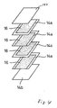
- a monolithic ceramic capacitor 10 shown in FIG. 2 was manufactured according to the following procedure.
- Barium carbonate (BaCO 3 ), titanium oxide (TiO 2 ), rare earth oxide (Re 2 O 3 ), vanadium oxide (V 2 O 5 ), copper oxide (CuO) and manganese carbonate (MnCO 3 ) were weighed so as to prepare dielectric ceramic compositions as shown in Table 1. Each composition was wet-milled with ethanol in a ball mill for 16 hours. The resultant mixture was dried and pulverized, followed by preliminary firing at a temperature of 1000°C to obtain a preliminary fired powder. An appropriate amount of polyvinyl alcohol solution was added to the powder and mixed. The mixture was sheeted through doctor blading to obtain a ceramic green sheet 14a having a thickness of 50 ⁇ m.
- an electroconductive paste consisting essentially of Pd-Ag was printed on the ceramic green sheet 14a to form thereon an electroconductive paste layer 16, which serves as an inner electrode. See FIG. 3.
- a plurality of the ceramic green sheets 14a each having the electroconductive paste layer 16 formed thereon were laminated in such a manner that the side of one sheet 14a having the electroconductive paste layer 16 exposed was alternated with that of another sheet 14a having the electroconductive paste layer 16 unexposed.
- This laminate was heated at 300°C in air, whereby the binder was burnt out, and was then fired for 2 hours.
- external electrodes 18 were applied to the corresponding sides of the laminate to thereby connect the exposed inner electrodes 16.
- a monolithic ceramic capacitor can be manufactured in a manner similar to that described above.
- the present invention provides a dielectric ceramic composition having a high specific inductive capacity, ⁇ r, of not lower than 30 or not lower than 40, and a large Q value of not smaller than 1000 at 1 MHz, and which is capable of being fired at a low temperature of up to 1250°C, i.e., capable of being applied to monolithic ceramic capacitors having inner electrodes made of Ag-Pd.
Landscapes
- Engineering & Computer Science (AREA)
- Chemical & Material Sciences (AREA)
- Ceramic Engineering (AREA)
- Power Engineering (AREA)
- Manufacturing & Machinery (AREA)
- Inorganic Chemistry (AREA)
- Microelectronics & Electronic Packaging (AREA)
- Materials Engineering (AREA)
- Structural Engineering (AREA)
- Organic Chemistry (AREA)
- Compositions Of Oxide Ceramics (AREA)
- Inorganic Insulating Materials (AREA)
Claims (20)
- Dielektrische keramische Zusammensetzung, umfassend eine Hauptkomponente der folgenden Formel:
xBaO - yTiO2 - z(RelaRell(1-a))2O3
wobei x, y und z in mol-% angegeben sind; x + y + z = 100; (x, y, z) in einen polygonalen Bereich, der durch die vier Punkte A (39,5, 59,5, 1), B (1, 59,5, 39,5), C (1, 85, 14) und D (14, 85, 1) definiert ist, fällt; 0,2 < a ≤1,0; Rel wenigstens ein Seltenerdelement, ausgewählt aus der Gruppe, bestehend aus Tb, Dy, Ho, Er und Yb, ist; und Rell wenigstens ein Seltenerdelement, ausgewählt aus der Gruppe, bestehend aus La, Pr, Nd und Sm, ist,
und ferner umfassend V als eine Nebenkomponente in einer Menge α von etwa 0,1 Gew.-% bis 15 Gew.-% in Form von V2O5, bezogen auf 100 Gew.-% der Hauptkomponente. - Dielektrische keramische Zusammensetzung nach Anspruch 1, wobei a gleich 1 ist.
- Dielektrische keramische Zusammensetzung nach Anspruch 2, die Cu als eine Nebenkomponente in einer Menge β von nicht mehr als etwa 10 Gew.-% in Form von CuO, bezogen auf 100 Gew.-% der Hauptkomponente, enthält.
- Dielektrische keramische Zusammensetzung nach Anspruch 2, die Mn als eine Nebenkomponente in einer Menge γ von nicht mehr als etwa 1 Gew.-% in Form von MnO, bezogen auf 100 Gew.-% der Hauptkomponente, enthält.
- Dielektrische keramische Zusammensetzung nach Anspruch 4, die Cu als eine Nebenkomponente in einer Menge β von nicht mehr als etwa 10 Gew.-% in Form von CuO, bezogen auf 100 Gew.-% der Hauptkomponente, enthält.
- Dielektrische keramische Zusammensetzung nach Anspruch 5, wobei α zwischen 2 und 4 liegt, β zwischen 2 und 4 liegt und γ nicht größer als etwa 0,05 ist.
- Dielektrische keramische Zusammensetzung nach Anspruch 6, wobei (x, y, z) etwa (10, 70, 20) ist und Rel wenigstens eines von Ho und Er ist.
- Dielektrische keramische Zusammensetzung nach Anspruch 1, wobei a kleiner als 1 ist.
- Dielektrische keramische Zusammensetzung nach Anspruch 8, die Cu als eine Nebenkomponente in einer Menge β von nicht mehr als etwa 10 Gew.-% in Form von CuO, bezogen auf 100 Gew.-% der Hauptkomponente, enthält.
- Dielektrische keramische Zusammensetzung nach Anspruch 8, die Mn als eine Nebenkomponente in einer Menge γ von nicht mehr als etwa 1 Gew.-% in Form von MnO, bezogen auf 100 Gew.-% der Hauptkomponente, enthält.
- Dielektrische keramische Zusammensetzung nach Anspruch 10, die Cu als eine Nebenkomponente in einer Menge β von nicht mehr als etwa 10 Gew.-% in Form von CuO, bezogen auf 100 Gew.-% der Hauptkomponente, enthält.
- Dielektrische keramische Zusammensetzung nach Anspruch 11, wobei α zwischen 2 und 4 liegt, β zwischen 2 und 4 liegt und γ nicht größer als etwa 0,05 ist.
- Monolithischer keramischer Kondensator, umfassend:eine keramische Schicht;eine Vielzahl innerer Elektroden, die im Inneren der keramischen Schicht eingebettet sind, wobei jede der Elektroden so angeordnet ist, dass sie von den anderen in der keramischen Schicht getrennt ist; undäußere Elektroden auf äußeren Oberflächen der keramischen Schicht, die mit den inneren Elektroden elektrisch leitend verbunden sind;wobei die keramische Schicht aus einer dielektrischen keramischen Zusammensetzung nach Anspruch 1 besteht.
- Monolithischer keramischer Kondensator nach Anspruch 13, wobei die inneren Elektroden Pd-Ag sind.
- Monolithischer keramischer Kondensator, umfassend:eine keramische Schicht;eine Vielzahl innerer Elektroden, die im Inneren der keramischen Schicht eingebettet sind, wobei jede der Elektroden so angeordnet ist, dass sie von den anderen in der keramischen Schicht getrennt ist; undäußere Elektroden auf äußeren Oberflächen der keramischen Schicht, die mit den inneren Elektroden elektrisch leitend verbunden sind;wobei die keramische Schicht aus einer dielektrischen keramischen Zusammensetzung nach Anspruch 2 besteht.
- Monolithischer keramischer Kondensator nach Anspruch 15, wobei die inneren Elektroden Pd-Ag sind.
- Monolithischer keramischer Kondensator, umfassend:eine keramische Schicht;eine Vielzahl innerer Elektroden, die im Inneren der keramischen Schicht eingebettet sind, wobei jede der Elektroden so angeordnet ist, dass sie von den anderen in der keramischen Schicht getrennt ist; undäußere Elektroden auf äußeren Oberflächen der keramischen Schicht, die mit den inneren Elektroden elektrisch leitend verbunden sind;wobei die keramische Schicht aus einer dielektrischen keramischen Zusammensetzung nach Anspruch 6 besteht.
- Monolithischer keramischer Kondensator, umfassend:eine keramische Schicht;eine Vielzahl innerer Elektroden, die im Inneren der keramischen Schicht eingebettet sind, wobei jede der Elektroden so angeordnet ist, dass sie von den anderen in der keramischen Schicht getrennt ist; undäußere Elektroden auf äußeren Oberflächen der keramischen Schicht, die mit den inneren Elektroden elektrisch leitend verbunden sind;wobei die keramische Schicht aus einer dielektrischen keramischen Zusammensetzung nach Anspruch 8 besteht.
- Monolithischer keramischer Kondensator nach Anspruch 18, wobei die inneren Elektroden Pd-Ag sind.
- Monolithischer keramischer Kondensator, umfassend:eine keramische Schicht;eine Vielzahl innerer Elektroden, die im Inneren der keramischen Schicht eingebettet sind, wobei jede der Elektroden so angeordnet ist, dass sie von den anderen in der keramischen Schicht getrennt ist; undäußere Elektroden auf äußeren Oberflächen der keramischen Schicht, die mit den inneren Elektroden elektrisch leitend verbunden sind;wobei die keramische Schicht aus einer dielektrischen keramischen Zusammensetzung nach Anspruch 11 besteht.
Applications Claiming Priority (3)
| Application Number | Priority Date | Filing Date | Title |
|---|---|---|---|
| JP26015097A JP3275799B2 (ja) | 1997-09-25 | 1997-09-25 | 誘電体磁器組成物 |
| JP26015097 | 1997-09-25 | ||
| JP260150/97 | 1997-09-25 |
Publications (3)
| Publication Number | Publication Date |
|---|---|
| EP0905724A2 EP0905724A2 (de) | 1999-03-31 |
| EP0905724A3 EP0905724A3 (de) | 2000-01-05 |
| EP0905724B1 true EP0905724B1 (de) | 2006-05-03 |
Family
ID=17344014
Family Applications (1)
| Application Number | Title | Priority Date | Filing Date |
|---|---|---|---|
| EP98118235A Expired - Lifetime EP0905724B1 (de) | 1997-09-25 | 1998-09-25 | Dielektrische keramische Zusammensetzung und dieselbe Verwendenter monolithischer keramischer Kondensator |
Country Status (6)
| Country | Link |
|---|---|
| US (1) | US6058005A (de) |
| EP (1) | EP0905724B1 (de) |
| JP (1) | JP3275799B2 (de) |
| KR (1) | KR100309159B1 (de) |
| CN (1) | CN1087867C (de) |
| DE (1) | DE69834373T2 (de) |
Families Citing this family (17)
| Publication number | Priority date | Publication date | Assignee | Title |
|---|---|---|---|---|
| JP2000143341A (ja) * | 1998-09-11 | 2000-05-23 | Murata Mfg Co Ltd | 誘電体セラミック組成物及び積層セラミック部品 |
| JP2000223351A (ja) * | 1999-01-28 | 2000-08-11 | Murata Mfg Co Ltd | 積層セラミックコンデンサ |
| CN1120137C (zh) * | 1999-02-19 | 2003-09-03 | 松下电器产业株式会社 | 电介质陶瓷组合物、使用该组合物的电容器及其制造方法 |
| US6291380B1 (en) * | 1999-03-15 | 2001-09-18 | Rohm Co., Ltd. | Dielectric ceramic and capacitor using the same |
| JP3348081B2 (ja) * | 1999-10-19 | 2002-11-20 | ティーディーケイ株式会社 | 誘電体磁器組成物および電子部品 |
| JP3367479B2 (ja) * | 1999-08-19 | 2003-01-14 | 株式会社村田製作所 | 誘電体セラミックおよび積層セラミック電子部品 |
| DE10043882B4 (de) * | 1999-09-07 | 2009-11-05 | Murata Mfg. Co., Ltd., Nagaokakyo-shi | Dielektrische Keramikzusammensetzung und monolithisches Keramikbauteil |
| US6377440B1 (en) | 2000-09-12 | 2002-04-23 | Paratek Microwave, Inc. | Dielectric varactors with offset two-layer electrodes |
| JP2002164247A (ja) * | 2000-11-24 | 2002-06-07 | Murata Mfg Co Ltd | 誘電体セラミック組成物および積層セラミックコンデンサ |
| DE60335427D1 (de) * | 2002-01-15 | 2011-02-03 | Tdk Corp | Dielektrische keramische Zusammensetzung und elektronische Vorrichtung |
| CN101006027B (zh) * | 2004-08-19 | 2010-05-05 | 株式会社村田制作所 | 介电陶瓷和单片陶瓷电容器 |
| CN100455539C (zh) * | 2006-08-02 | 2009-01-28 | 南京工业大学 | 一种微波介质陶瓷及其制备方法 |
| EP2236589B1 (de) | 2007-11-22 | 2016-09-21 | Idemitsu Kosan Co., Ltd. | Schmierölzusammensetzung für kältemaschine |
| JP5612250B2 (ja) | 2008-03-07 | 2014-10-22 | 出光興産株式会社 | 冷凍機用潤滑油組成物 |
| WO2010013414A1 (ja) * | 2008-07-29 | 2010-02-04 | 株式会社村田製作所 | 積層セラミックコンデンサ |
| KR101113441B1 (ko) * | 2009-12-31 | 2012-02-29 | 삼성전기주식회사 | 유전체 자기 조성물 및 이를 포함하는 적층 세라믹 커패시터 |
| JP5673595B2 (ja) * | 2012-04-19 | 2015-02-18 | 株式会社村田製作所 | 積層型セラミック電子部品およびその実装構造体 |
Family Cites Families (10)
| Publication number | Priority date | Publication date | Assignee | Title |
|---|---|---|---|---|
| JPS529319B2 (de) * | 1972-09-28 | 1977-03-15 | ||
| JPS56162820A (en) * | 1980-05-20 | 1981-12-15 | Kiyoshi Okazaki | Vapor bank layered laminated ceramic capacitor and method of manufacturing same |
| JPS5873908A (ja) * | 1981-10-28 | 1983-05-04 | ティーディーケイ株式会社 | 高周波用誘電体磁器組成物 |
| JPH02267166A (ja) * | 1989-04-07 | 1990-10-31 | Matsushita Electric Ind Co Ltd | 積層セラミックコンデンサ |
| US5244851A (en) * | 1991-02-28 | 1993-09-14 | Sanyo Electric Co., Ltd. | Microwave dielectric ceramic composition |
| JP2613722B2 (ja) * | 1991-09-27 | 1997-05-28 | 日本碍子株式会社 | 低温焼成用誘電体磁器組成物の製造法 |
| JP3028503B2 (ja) * | 1992-01-31 | 2000-04-04 | 株式会社村田製作所 | 非還元性誘電体磁器組成物 |
| JP2625074B2 (ja) * | 1992-06-24 | 1997-06-25 | 京セラ株式会社 | 誘電体磁器組成物および誘電体共振器 |
| US5688732A (en) * | 1994-11-16 | 1997-11-18 | Electronics & Telecommunications Research Inst. | Dielectric ceramic compositions for microwave |
| US5916834A (en) * | 1996-12-27 | 1999-06-29 | Kyocera Corporation | Dielectric ceramics |
-
1997
- 1997-09-25 JP JP26015097A patent/JP3275799B2/ja not_active Expired - Fee Related
-
1998
- 1998-08-28 US US09/141,657 patent/US6058005A/en not_active Expired - Lifetime
- 1998-09-23 KR KR1019980039381A patent/KR100309159B1/ko not_active Expired - Fee Related
- 1998-09-25 DE DE69834373T patent/DE69834373T2/de not_active Expired - Lifetime
- 1998-09-25 EP EP98118235A patent/EP0905724B1/de not_active Expired - Lifetime
- 1998-09-25 CN CN98120760A patent/CN1087867C/zh not_active Expired - Fee Related
Also Published As
| Publication number | Publication date |
|---|---|
| CN1212439A (zh) | 1999-03-31 |
| CN1087867C (zh) | 2002-07-17 |
| KR19990030058A (ko) | 1999-04-26 |
| DE69834373D1 (de) | 2006-06-08 |
| JP3275799B2 (ja) | 2002-04-22 |
| DE69834373T2 (de) | 2006-09-28 |
| US6058005A (en) | 2000-05-02 |
| KR100309159B1 (ko) | 2002-01-17 |
| EP0905724A3 (de) | 2000-01-05 |
| JPH11100263A (ja) | 1999-04-13 |
| EP0905724A2 (de) | 1999-03-31 |
Similar Documents
| Publication | Publication Date | Title |
|---|---|---|
| KR100259321B1 (ko) | 유전체 세라믹 조성물 및 이를 이용한 적층 세라믹 커패시터 | |
| KR100313234B1 (ko) | 유전체 세라믹 조성물 및 적층 세라믹 커패시터 | |
| US6522521B2 (en) | Reduction-resistant dielectric ceramic compact and laminated ceramic capacitor | |
| JP3039417B2 (ja) | 積層セラミックコンデンサ | |
| JP2998639B2 (ja) | 積層セラミックコンデンサ | |
| JP3024536B2 (ja) | 積層セラミックコンデンサ | |
| JP2993425B2 (ja) | 積層セラミックコンデンサ | |
| JP3039397B2 (ja) | 誘電体磁器組成物とそれを用いた積層セラミックコンデンサ | |
| EP0905724B1 (de) | Dielektrische keramische Zusammensetzung und dieselbe Verwendenter monolithischer keramischer Kondensator | |
| KR100375719B1 (ko) | 유전체 세라믹 조성물 및 모놀리식 세라믹 커패시터 | |
| US6385035B1 (en) | Dielectric ceramic composition and monolithic ceramic component | |
| JP3336967B2 (ja) | 積層セラミックコンデンサ | |
| JP2000143341A (ja) | 誘電体セラミック組成物及び積層セラミック部品 | |
| KR980009197A (ko) | 적층 세라믹 커패시터 | |
| JP3039409B2 (ja) | 積層セラミックコンデンサ | |
| EP1056102B1 (de) | Nichtreduzierende dielektrische keramische Zusammensetzung und monolithischer keramischer Kondensator | |
| JP3678072B2 (ja) | 誘電体セラミック組成物及び積層セラミック部品 | |
| JP3678073B2 (ja) | 誘電体セラミック組成物及び積層セラミック部品 | |
| KR102923425B1 (ko) | 고온 안정성을 갖는 유전체 조성물 및 이를 포함하는 적층 세라믹 커패시터 | |
| JPH10172857A (ja) | 積層セラミックコンデンサ | |
| JPH10172858A (ja) | 積層セラミックコンデンサ |
Legal Events
| Date | Code | Title | Description |
|---|---|---|---|
| PUAI | Public reference made under article 153(3) epc to a published international application that has entered the european phase |
Free format text: ORIGINAL CODE: 0009012 |
|
| 17P | Request for examination filed |
Effective date: 19980925 |
|
| AK | Designated contracting states |
Kind code of ref document: A2 Designated state(s): DE FR GB |
|
| AX | Request for extension of the european patent |
Free format text: AL;LT;LV;MK;RO;SI |
|
| PUAL | Search report despatched |
Free format text: ORIGINAL CODE: 0009013 |
|
| AK | Designated contracting states |
Kind code of ref document: A3 Designated state(s): AT BE CH CY DE DK ES FI FR GB GR IE IT LI LU MC NL PT SE |
|
| AX | Request for extension of the european patent |
Free format text: AL;LT;LV;MK;RO;SI |
|
| AKX | Designation fees paid |
Free format text: DE FR GB |
|
| GRAP | Despatch of communication of intention to grant a patent |
Free format text: ORIGINAL CODE: EPIDOSNIGR1 |
|
| GRAS | Grant fee paid |
Free format text: ORIGINAL CODE: EPIDOSNIGR3 |
|
| GRAA | (expected) grant |
Free format text: ORIGINAL CODE: 0009210 |
|
| AK | Designated contracting states |
Kind code of ref document: B1 Designated state(s): DE FR GB |
|
| REG | Reference to a national code |
Ref country code: GB Ref legal event code: FG4D |
|
| REF | Corresponds to: |
Ref document number: 69834373 Country of ref document: DE Date of ref document: 20060608 Kind code of ref document: P |
|
| PLBE | No opposition filed within time limit |
Free format text: ORIGINAL CODE: 0009261 |
|
| STAA | Information on the status of an ep patent application or granted ep patent |
Free format text: STATUS: NO OPPOSITION FILED WITHIN TIME LIMIT |
|
| 26N | No opposition filed |
Effective date: 20070206 |
|
| EN | Fr: translation not filed | ||
| GBPC | Gb: european patent ceased through non-payment of renewal fee |
Effective date: 20060925 |
|
| PG25 | Lapsed in a contracting state [announced via postgrant information from national office to epo] |
Ref country code: GB Free format text: LAPSE BECAUSE OF NON-PAYMENT OF DUE FEES Effective date: 20060925 |
|
| PG25 | Lapsed in a contracting state [announced via postgrant information from national office to epo] |
Ref country code: FR Free format text: LAPSE BECAUSE OF FAILURE TO SUBMIT A TRANSLATION OF THE DESCRIPTION OR TO PAY THE FEE WITHIN THE PRESCRIBED TIME-LIMIT Effective date: 20070309 |
|
| PG25 | Lapsed in a contracting state [announced via postgrant information from national office to epo] |
Ref country code: FR Free format text: LAPSE BECAUSE OF FAILURE TO SUBMIT A TRANSLATION OF THE DESCRIPTION OR TO PAY THE FEE WITHIN THE PRESCRIBED TIME-LIMIT Effective date: 20060503 |
|
| PGFP | Annual fee paid to national office [announced via postgrant information from national office to epo] |
Ref country code: DE Payment date: 20130918 Year of fee payment: 16 |
|
| REG | Reference to a national code |
Ref country code: DE Ref legal event code: R119 Ref document number: 69834373 Country of ref document: DE |
|
| REG | Reference to a national code |
Ref country code: DE Ref legal event code: R119 Ref document number: 69834373 Country of ref document: DE Effective date: 20150401 |
|
| PG25 | Lapsed in a contracting state [announced via postgrant information from national office to epo] |
Ref country code: DE Free format text: LAPSE BECAUSE OF NON-PAYMENT OF DUE FEES Effective date: 20150401 |