EP0905799B1 - Herstellungsverfahren einer optischen Halbleitervorrichtung - Google Patents
Herstellungsverfahren einer optischen Halbleitervorrichtung Download PDFInfo
- Publication number
- EP0905799B1 EP0905799B1 EP98307849A EP98307849A EP0905799B1 EP 0905799 B1 EP0905799 B1 EP 0905799B1 EP 98307849 A EP98307849 A EP 98307849A EP 98307849 A EP98307849 A EP 98307849A EP 0905799 B1 EP0905799 B1 EP 0905799B1
- Authority
- EP
- European Patent Office
- Prior art keywords
- facet orientation
- layer
- light emitting
- gan
- emitting layer
- Prior art date
- Legal status (The legal status is an assumption and is not a legal conclusion. Google has not performed a legal analysis and makes no representation as to the accuracy of the status listed.)
- Expired - Lifetime
Links
Images


Classifications
-
- H—ELECTRICITY
- H10—SEMICONDUCTOR DEVICES; ELECTRIC SOLID-STATE DEVICES NOT OTHERWISE PROVIDED FOR
- H10H—INORGANIC LIGHT-EMITTING SEMICONDUCTOR DEVICES HAVING POTENTIAL BARRIERS
- H10H20/00—Individual inorganic light-emitting semiconductor devices having potential barriers, e.g. light-emitting diodes [LED]
- H10H20/80—Constructional details
- H10H20/81—Bodies
- H10H20/822—Materials of the light-emitting regions
- H10H20/824—Materials of the light-emitting regions comprising only Group III-V materials, e.g. GaP
- H10H20/825—Materials of the light-emitting regions comprising only Group III-V materials, e.g. GaP containing nitrogen, e.g. GaN
-
- B—PERFORMING OPERATIONS; TRANSPORTING
- B82—NANOTECHNOLOGY
- B82Y—SPECIFIC USES OR APPLICATIONS OF NANOSTRUCTURES; MEASUREMENT OR ANALYSIS OF NANOSTRUCTURES; MANUFACTURE OR TREATMENT OF NANOSTRUCTURES
- B82Y20/00—Nanooptics, e.g. quantum optics or photonic crystals
-
- H—ELECTRICITY
- H01—ELECTRIC ELEMENTS
- H01S—DEVICES USING THE PROCESS OF LIGHT AMPLIFICATION BY STIMULATED EMISSION OF RADIATION [LASER] TO AMPLIFY OR GENERATE LIGHT; DEVICES USING STIMULATED EMISSION OF ELECTROMAGNETIC RADIATION IN WAVE RANGES OTHER THAN OPTICAL
- H01S5/00—Semiconductor lasers
- H01S5/30—Structure or shape of the active region; Materials used for the active region
- H01S5/32—Structure or shape of the active region; Materials used for the active region comprising PN junctions, e.g. hetero- or double- heterostructures
- H01S5/3202—Structure or shape of the active region; Materials used for the active region comprising PN junctions, e.g. hetero- or double- heterostructures grown on specifically orientated substrates, or using orientation dependent growth
- H01S5/32025—Structure or shape of the active region; Materials used for the active region comprising PN junctions, e.g. hetero- or double- heterostructures grown on specifically orientated substrates, or using orientation dependent growth non-polar orientation
-
- H—ELECTRICITY
- H01—ELECTRIC ELEMENTS
- H01S—DEVICES USING THE PROCESS OF LIGHT AMPLIFICATION BY STIMULATED EMISSION OF RADIATION [LASER] TO AMPLIFY OR GENERATE LIGHT; DEVICES USING STIMULATED EMISSION OF ELECTROMAGNETIC RADIATION IN WAVE RANGES OTHER THAN OPTICAL
- H01S5/00—Semiconductor lasers
- H01S5/30—Structure or shape of the active region; Materials used for the active region
- H01S5/34—Structure or shape of the active region; Materials used for the active region comprising quantum well or superlattice structures, e.g. single quantum well [SQW] lasers, multiple quantum well [MQW] lasers or graded index separate confinement heterostructure [GRINSCH] lasers
- H01S5/343—Structure or shape of the active region; Materials used for the active region comprising quantum well or superlattice structures, e.g. single quantum well [SQW] lasers, multiple quantum well [MQW] lasers or graded index separate confinement heterostructure [GRINSCH] lasers in AIIIBV compounds, e.g. AlGaAs-laser, InP-based laser
-
- H—ELECTRICITY
- H10—SEMICONDUCTOR DEVICES; ELECTRIC SOLID-STATE DEVICES NOT OTHERWISE PROVIDED FOR
- H10H—INORGANIC LIGHT-EMITTING SEMICONDUCTOR DEVICES HAVING POTENTIAL BARRIERS
- H10H20/00—Individual inorganic light-emitting semiconductor devices having potential barriers, e.g. light-emitting diodes [LED]
- H10H20/80—Constructional details
- H10H20/81—Bodies
- H10H20/817—Bodies characterised by the crystal structures or orientations, e.g. polycrystalline, amorphous or porous
-
- H—ELECTRICITY
- H01—ELECTRIC ELEMENTS
- H01S—DEVICES USING THE PROCESS OF LIGHT AMPLIFICATION BY STIMULATED EMISSION OF RADIATION [LASER] TO AMPLIFY OR GENERATE LIGHT; DEVICES USING STIMULATED EMISSION OF ELECTROMAGNETIC RADIATION IN WAVE RANGES OTHER THAN OPTICAL
- H01S5/00—Semiconductor lasers
- H01S5/0014—Measuring characteristics or properties thereof
- H01S5/0035—Simulations of laser characteristics
-
- H—ELECTRICITY
- H01—ELECTRIC ELEMENTS
- H01S—DEVICES USING THE PROCESS OF LIGHT AMPLIFICATION BY STIMULATED EMISSION OF RADIATION [LASER] TO AMPLIFY OR GENERATE LIGHT; DEVICES USING STIMULATED EMISSION OF ELECTROMAGNETIC RADIATION IN WAVE RANGES OTHER THAN OPTICAL
- H01S5/00—Semiconductor lasers
- H01S5/02—Structural details or components not essential to laser action
- H01S5/0206—Substrates, e.g. growth, shape, material, removal or bonding
- H01S5/021—Silicon based substrates
-
- H—ELECTRICITY
- H01—ELECTRIC ELEMENTS
- H01S—DEVICES USING THE PROCESS OF LIGHT AMPLIFICATION BY STIMULATED EMISSION OF RADIATION [LASER] TO AMPLIFY OR GENERATE LIGHT; DEVICES USING STIMULATED EMISSION OF ELECTROMAGNETIC RADIATION IN WAVE RANGES OTHER THAN OPTICAL
- H01S5/00—Semiconductor lasers
- H01S5/02—Structural details or components not essential to laser action
- H01S5/0206—Substrates, e.g. growth, shape, material, removal or bonding
- H01S5/0213—Sapphire, quartz or diamond based substrates
-
- H—ELECTRICITY
- H01—ELECTRIC ELEMENTS
- H01S—DEVICES USING THE PROCESS OF LIGHT AMPLIFICATION BY STIMULATED EMISSION OF RADIATION [LASER] TO AMPLIFY OR GENERATE LIGHT; DEVICES USING STIMULATED EMISSION OF ELECTROMAGNETIC RADIATION IN WAVE RANGES OTHER THAN OPTICAL
- H01S5/00—Semiconductor lasers
- H01S5/04—Processes or apparatus for excitation, e.g. pumping, e.g. by electron beams
- H01S5/042—Electrical excitation ; Circuits therefor
- H01S5/0425—Electrodes, e.g. characterised by the structure
- H01S5/04256—Electrodes, e.g. characterised by the structure characterised by the configuration
- H01S5/04257—Electrodes, e.g. characterised by the structure characterised by the configuration having positive and negative electrodes on the same side of the substrate
-
- H—ELECTRICITY
- H01—ELECTRIC ELEMENTS
- H01S—DEVICES USING THE PROCESS OF LIGHT AMPLIFICATION BY STIMULATED EMISSION OF RADIATION [LASER] TO AMPLIFY OR GENERATE LIGHT; DEVICES USING STIMULATED EMISSION OF ELECTROMAGNETIC RADIATION IN WAVE RANGES OTHER THAN OPTICAL
- H01S5/00—Semiconductor lasers
- H01S5/30—Structure or shape of the active region; Materials used for the active region
- H01S5/32—Structure or shape of the active region; Materials used for the active region comprising PN junctions, e.g. hetero- or double- heterostructures
- H01S5/3201—Structure or shape of the active region; Materials used for the active region comprising PN junctions, e.g. hetero- or double- heterostructures incorporating bulkstrain effects, e.g. strain compensation, strain related to polarisation
-
- H—ELECTRICITY
- H01—ELECTRIC ELEMENTS
- H01S—DEVICES USING THE PROCESS OF LIGHT AMPLIFICATION BY STIMULATED EMISSION OF RADIATION [LASER] TO AMPLIFY OR GENERATE LIGHT; DEVICES USING STIMULATED EMISSION OF ELECTROMAGNETIC RADIATION IN WAVE RANGES OTHER THAN OPTICAL
- H01S5/00—Semiconductor lasers
- H01S5/30—Structure or shape of the active region; Materials used for the active region
- H01S5/32—Structure or shape of the active region; Materials used for the active region comprising PN junctions, e.g. hetero- or double- heterostructures
- H01S5/3202—Structure or shape of the active region; Materials used for the active region comprising PN junctions, e.g. hetero- or double- heterostructures grown on specifically orientated substrates, or using orientation dependent growth
- H01S5/320275—Structure or shape of the active region; Materials used for the active region comprising PN junctions, e.g. hetero- or double- heterostructures grown on specifically orientated substrates, or using orientation dependent growth semi-polar orientation
-
- H—ELECTRICITY
- H01—ELECTRIC ELEMENTS
- H01S—DEVICES USING THE PROCESS OF LIGHT AMPLIFICATION BY STIMULATED EMISSION OF RADIATION [LASER] TO AMPLIFY OR GENERATE LIGHT; DEVICES USING STIMULATED EMISSION OF ELECTROMAGNETIC RADIATION IN WAVE RANGES OTHER THAN OPTICAL
- H01S5/00—Semiconductor lasers
- H01S5/30—Structure or shape of the active region; Materials used for the active region
- H01S5/34—Structure or shape of the active region; Materials used for the active region comprising quantum well or superlattice structures, e.g. single quantum well [SQW] lasers, multiple quantum well [MQW] lasers or graded index separate confinement heterostructure [GRINSCH] lasers
- H01S5/343—Structure or shape of the active region; Materials used for the active region comprising quantum well or superlattice structures, e.g. single quantum well [SQW] lasers, multiple quantum well [MQW] lasers or graded index separate confinement heterostructure [GRINSCH] lasers in AIIIBV compounds, e.g. AlGaAs-laser, InP-based laser
- H01S5/34333—Structure or shape of the active region; Materials used for the active region comprising quantum well or superlattice structures, e.g. single quantum well [SQW] lasers, multiple quantum well [MQW] lasers or graded index separate confinement heterostructure [GRINSCH] lasers in AIIIBV compounds, e.g. AlGaAs-laser, InP-based laser with a well layer based on Ga(In)N or Ga(In)P, e.g. blue laser
-
- H—ELECTRICITY
- H10—SEMICONDUCTOR DEVICES; ELECTRIC SOLID-STATE DEVICES NOT OTHERWISE PROVIDED FOR
- H10H—INORGANIC LIGHT-EMITTING SEMICONDUCTOR DEVICES HAVING POTENTIAL BARRIERS
- H10H20/00—Individual inorganic light-emitting semiconductor devices having potential barriers, e.g. light-emitting diodes [LED]
- H10H20/80—Constructional details
- H10H20/81—Bodies
- H10H20/817—Bodies characterised by the crystal structures or orientations, e.g. polycrystalline, amorphous or porous
- H10H20/818—Bodies characterised by the crystal structures or orientations, e.g. polycrystalline, amorphous or porous within the light-emitting regions
-
- H—ELECTRICITY
- H10—SEMICONDUCTOR DEVICES; ELECTRIC SOLID-STATE DEVICES NOT OTHERWISE PROVIDED FOR
- H10H—INORGANIC LIGHT-EMITTING SEMICONDUCTOR DEVICES HAVING POTENTIAL BARRIERS
- H10H20/00—Individual inorganic light-emitting semiconductor devices having potential barriers, e.g. light-emitting diodes [LED]
- H10H20/80—Constructional details
- H10H20/81—Bodies
- H10H20/819—Bodies characterised by their shape, e.g. curved or truncated substrates
- H10H20/821—Bodies characterised by their shape, e.g. curved or truncated substrates of the light-emitting regions, e.g. non-planar junctions
Definitions
- the present invention relates to optical semiconductor devices, for example to a structure for improving the efficiency of light emitters and photodetectors fabricated from GaN-based semiconductors.
- III-N semiconductor is a semiconductor having a Group III element and nitrogen.
- III-N semiconductors such as GaN are useful in fabricating light emitting elements that emit in the blue and violet regions of the optical spectrum. These elements include light emitting diodes and laser diodes.
- Laser diodes that use semiconductor material based on GaN that emit in the blue and violet regions of the spectrum hold the promise of substantially improving the amount of information that can be stored on an optical disk.
- higher efficiencies are needed for both semiconductor light emitters and photodetectors.
- GaN-based optical semiconductor devices using BN, AIN, GaN, or InN, which are compounds of nitrogen and Group III elements such as B, Al, Ga, and In and their mixed crystal semiconductors (hereinafter, called GaN-based semiconductors).
- Light emitting elements based on III-N semiconductors are typically fabricated by creating a p-n diode structure having a light generating region between the p-type and n-type layers.
- the diode is constructed from layers of III-N semiconducting materials. After the appropriate layers are grown, electrodes are formed on the p-type and n-type layers to provide the electrical connections for driving the light-emitting element.
- LEDs blue and green light-emitting diodes
- LDs short-wavelength laser diodes
- GaInN/GaN strained quantum wells GaInN/GaInNstrainedquantum wells located between the n-type and p-type layers to generate light by the recombination of holes and electrons injected from these layers.
- a strained GaN-based semiconductor layer is constructed by growing a ⁇ 0001 ⁇ plane of a normal GaN-based crystal. The resulting layer has a large piezoelectric field. For example, in a Ga 0.9 In 0.1 N strained layer, an extremely large piezoelectric field of around 1 MV/cm is generated.
- the energy band of the quantum well layer tends to increase as the electric field increases.
- the wave functions of the electrons and holes alternately polarise, and the overlap integrals of both wave functions decrease. Since the optical properties such as the light emission and absorption efficiencies depend on these overlap integrals, the efficiency of these devices decreases with increasing electric fields.
- an optical semiconductor device including a plurality of GaN-based semiconductor layers containing a strained quantum well layer, said strained quantum well layer having a piezoelectric field therein having a field strength that depends on the growth orientation of said strained quantum well layer, wherein said quantum layer has a growth orientation at which said piezoelectric field strength will be less than the maximum value of said piezoelectric field strength as a function of said orientation.
- WO 96/24167 discloses a green-blue to ultraviolet light-emitting semiconductor laser having a top contact, top Bragg reflector, bottom Bragg reflector, cladding layer, active layer, cladding layer, buffer, substrate, bottom contact and passivation layer.
- a Ga*N material on a base structure comprises a SiC substrate selected from the group consisting of 2H-SiC, 4H-SiC and a-axis oriented 6H-SiC.
- Cladding layers have larger band gaps than the active layer and are complementarily doped.
- EP 0 743 727 discloses a GaN system compound semiconductor double heterostructure in a light emission device comprising an active layer sandwiched between first and second cladding layers. Those three layers are made of GaN system compound semiconductor materials.
- the first, second and third GaN system compound semiconductor materials have first, second and third hexagonal crystal structures of basal planes tilted from a (0001) plane by an angle in the range of 0 degree to a few degrees, and the basal planes are substantially parallel to interfaces of the active layer to the first and second cladding layers.
- the GaN system compound semiconductor double heterostructure has a pair of opposite resonance faces vertical to a direction in which a light is emitted, and for each of the first, second and third hexagonal crystal structures, a pair of opposite planes in the six planes vertical to the basal plane forms the opposite resonance faces.
- the double heterostucture is formed on a GaN epitaxial layer by selective area growth.
- EP 0 716 457 discloses a nitride semiconductor light-emitting device having an active layer of a single-quantum well structure or multi-quantum well made of a nitride semiconductor containing indium and gallium.
- a first p-type clad layer made of a p-type nitride semiconductor containing aluminium and gallium is provided in contact with one surface of the active layer.
- a second p-type clad layer made of a p-type nitride semiconductor containing aluminium and gallium is provided on the first p-type clad layer.
- the second p-type clad layer has a larger band gap than that of the first p-type clad layer.
- An n-type semiconductor layer is provided in contact with the other surface of the active layer.
- Niwa et al disclose a laser diode based on wurtzite GaN in which GaN/AlGaN strained quantum wells are grown along the direction perpendicular to the ⁇ 0001 ⁇ axis.
- the present invention seeks to provide an improved optical semiconductor device.
- the preferred embodiment can provide an improved III-N semiconductor device in which the efficiency of light generation or detection is increased relative to prior art devices. It can also provide a strained quantum well layer having a reduced piezoelectric field.
- the preferred embodiment is an optical semiconductor device having a plurality of GaN-based semiconductor layers containing a strained quantum well layer in which the strained quantum well layer has a piezoelectric field that depends on the orientation of the strained quantum well layer when the quantum layer is grown.
- the strained quantum well layer is grown with an orientation at which the piezoelectric field is less than the maximum value of the piezoelectric field strength as a function of the orientation.
- the growth orientation of the strained quantum well layer is tilted by about 40°, 90° or 140° from the ⁇ 0001 ⁇ direction of the wurtzite crystal structure.
- the growth orientation of the strained quantum well layer is tilted at least 1° from the ⁇ 111 ⁇ direction of the zincblende crystal structure.
- the growth orientation is chosen to minimise the piezoelectric field in the strained quantum well layer.
- the described embodiment is based on the observation that the piezoelectric field in a strained quantum well layer depends on the orientation of the crystal structure of the quantum well layer, and hence, by controlling the facet orientation, the piezoelectric field can be minimised.
- the manner in which this is accomplished may be more easily understood with reference to two types of strained quantum well structures, those based on a wurtzite crystal structure and those based on a zincblende crystal structure.
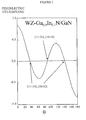
- FIG. 1 illustrates a wurtzite crystal GaN (WZ-GaN) structure 10.
- the piezoelectric field generated in a crystal having a facet orientation along are 11 in Figure 1 is shown in Figure 2 as a function of the angle ⁇ between the ⁇ 0001 ⁇ direction and the facet orientation.
- the data shown in Figure 2 is for Ga 0.9 In 0.1 N strained quantum well layers.
- the piezoelectric field reaches maxima in the ⁇ 0001 ⁇ direction or the ⁇ 000-1 ⁇ direction, and has three orientations at which the piezoelectric field is zero.
- the same result is obtained for other arcs. e.g., arc 12. That is, the piezoelectric field is uniquely determined by the difference in the angle between the ⁇ 0001 ⁇ direction and the facet orientation of the concerned plane.
- the strength of the piezoelectric field depends on the composition of the GalnN strained quantum well layer.
- the plane orientations in which the field is zero are, at most, only slightly altered.
- the 90° facet orientation measured from the ⁇ 0001 ⁇ direction where the piezoelectric field becomes 0 does not depend on the ratio of Ga to In.
- the plane orientations corresponding to the 40° and 140° orientations discussed above change by no more than a maximum of 5° from the 40° and 140° values determined for the composition shown in Figure 2.
- ZB-GaN zincblende crystal structure GaN-based semiconductor layer
- a ZB-Ga 0.9 In 0.1 N strained quantum well layer can be formed on GaN in a manner analogous to the WZ-GaN-based semiconductor strained quantum well layer discussed above.
- Figure 3 shows the crystal structure 20 of the ZB-GaN-based semiconductor.
- the radius vector has a polar angle ⁇ measured from the ⁇ 001 ⁇ direction and a cone angle. ⁇ , about the ⁇ 001 ⁇ direction.
- First and second paths having a constant azimuth angle ⁇ are shown at 21 and 22.
- Figure 4 is a plot of the piezoelectric field in the strained quantum well layer with respect to the polar angle ⁇ for various orientations of the strained quantum well layer on path 21.
- a strained quantum well crystal of ZB-GaN-based semiconductor almost no piezoelectric field is generated in the strained quantum well layer that has growth planes beginning in the ⁇ 001 ⁇ plane or ⁇ 011 ⁇ plane and a facet orientation angle ⁇ on path 22.
- Figure 5 is a cross-sectional view of a laser 30 not in accordance with the invention. If the crystal growth orientation is excluded, the composition of each deposited layer is essentially that used in a conventional laser diode.
- Laser 30 is constructed from a number of layers.
- An n-type GaN contact layer 33, an n-type AIGaN cladding layer 34, a strained multiple quantum well layer 35, a p-type AlGaN cladding layer 36, and a p-type GaN contact layer 37 are successively deposited on a substrate 31 which is typically, sapphire, SiC, or GaN.
- An n-electrode 38 and a p-electrode 39 are deposited as shown.
- the strained multiple quantum well layer 35 is typically constructed from GaInN/GaN or GaInN/GaInN.
- the layers of the quantum well are caused to grow such that the piezoelectric field generated by the layers is negligible.
- the ⁇ 0001 ⁇ plane of a sapphire substrate is used to grow the various layers. As noted above, this leads to a high piezoelectric field and poor efficiency.
- the piezoelectric field is substantially zero.
- One of these is utilised in a laser diode.
- the particular plane will depend on the type of crystal.
- the ⁇ 2-1-10 ⁇ plane of the strained quantum layer material can be caused to grow by selecting the appropriate growing surface of substrate 31. If the substrate is sapphire, the sapphire is cut such that the ⁇ 01-12 ⁇ plane is used for growing layer 33.
- the ⁇ 2-1-10 ⁇ plane is used. SiC with a growth plane of ⁇ 2-1-10 ⁇ is preferred.
- the preferred embodiment may also be utilised to provide improved performance from photodetectors.
- Photodetectors fabricated by growing the device on the ⁇ 0001 ⁇ plane of a sapphire substrate exhibit an efficiency and absorption band that depend on light intensity. In particular, the efficiency of conversion increases with light intensity while the useful wavelength range decreases.
- the device is grown on a substrate that results in little or no piezoelectric field in the strained quantum well layer. Hence, the increase in efficiency and decrease in absorption band are substantially reduced or eliminated.
- the growing technique for a photodetector is the same as that used to construct a light emitter; however, thicker strained quantum well layers are utilised to improve the absorption of the incident light.
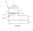
- FIG. 7 is a cross-sectional view of the optical semiconductor device 50 according to an embodiment of the present invention in which only the layers related solely to light emission and absorption have the desired facet orientation.
- Device 50 is constructed by growing an n-type GaN contact layer 53 and an n-type AlGaN cladding layer 54 on the ⁇ 0001 ⁇ plane orientation on the substrate 51 such as SiC or GaN based on conventional technology. Next, by selective growing or selective etching, the ⁇ 2-1-14 ⁇ plane or ⁇ 01-12 ⁇ plane is formed.
- the GaInN/GaN or GaInN/GaInN strained multiple quantum well layer 55 is then formed by repeating the crystal growth.
- the remaining p-type AlGaN cladding layer 56 and the p-type GaN contact layer 57 are successively deposited and formed.
- the p-type AlGaN cladding layer 56 and the p-type GaN contact layer 57 change the crystal structure back to that corresponding to the ⁇ 0001 ⁇ plane from the facet orientation of the well layer 55 and become layers with specific thicknesses.
- the n-electrode 58 and the p-electrode 59 are formed as the electrodes on the n-type GaN contact layer 53 and the p-type GaN contact layer 57, respectively.
- the growing surfaces 55A, 55B on both sides of the GaInN strained multiple quantum well layer 55 are the ⁇ 01-l2 ⁇ plane or the ⁇ 2-1-14 ⁇ plane.
- the p-type AlGaN cladding layer 56 and the p-type GaN contact layer 57 become flat growing surfaces. To simplify the next process, it is advisable that they be several microns thick.
- an AlN buffer layer 52 is grown on the substrate 51.
- the specific plane selected for growing the quantum well layer depends on the crystal type.
- the ⁇ 001 ⁇ plane may be utilised, since this plane has excellent crystal quality and generates almost no piezoelectric field.
- the piezoelectric field as a function of the facet orientation behaves similarly to that described above if the crystal type is the same.
- the orientation inclination, ⁇ , for which the piezoelectric field of 0 may, however, change by as much as 10°.
Landscapes
- Physics & Mathematics (AREA)
- Optics & Photonics (AREA)
- General Physics & Mathematics (AREA)
- Chemical & Material Sciences (AREA)
- Engineering & Computer Science (AREA)
- Nanotechnology (AREA)
- Condensed Matter Physics & Semiconductors (AREA)
- Electromagnetism (AREA)
- Biophysics (AREA)
- Crystallography & Structural Chemistry (AREA)
- Life Sciences & Earth Sciences (AREA)
- Led Devices (AREA)
- Semiconductor Lasers (AREA)
- Light Receiving Elements (AREA)
- Recrystallisation Techniques (AREA)
Claims (8)
- Verfahren zum Herstellen einer Licht emittierenden Halbleitervorrichtung (50) mit einer verspannten Quantenschacht-III-Nitrid Licht emittierenden Schicht (55), welches Verfahren umfasst:Auswählen einer Facettenorientierung der III-Nitrid Licht emittierenden Schicht zum Steuern und/oder Regeln einer Feldstärke eines piezoelektrischen Feldes darin; undWachsenlassen der III-Nitrid Licht emittierenden Schicht mit einer Wurtzit-Kristallstruktur mit der ausgewählten Facettenorientierung, wobei die ausgewählte Facettenorientierung bezogen auf die {0001}-Richtung der Wurtzit-Kristallstruktur unter einem Winkel, welcher so gewählt ist, dass die piezoelektrische Feldstärke in der Licht emittierenden Schicht vernachlässigbar ist, geneigt wird, wobei der Winkel ausgewählt wird aus ungefähr 40°, 90° oder 140° im Fall einer GaN-basierten Licht emittierenden Schicht,wobei das Verfahren ferner umfasst das Bereitstellen eines Substrats (51) mit einer ersten Facettenorientierung;das Wachsenlassen einer ersten Halbleiterschicht (54) auf dem Substrat, wobei die erste Halbleiterschicht wachsen gelassen wird mit der ersten sich von der ausgewählten Facettenorientierung unterscheidenden Facettenorientierung;Verändern einer exponierten Oberfläche der ersten Halbleiterschicht zum Bereitstellen einer Oberfläche, welche die gewählte Facettenorientierung aufweist; undWachsenlassen der Licht emittierenden Schicht (55) auf der Oberfläche, welche die ausgewählte Facettenorientierung aufweist.
- Verfahren nach Anspruch 1, bei welchem das Substrat Saphir, SiC oder GaN ist.
- Verfahren nach Anspruch 1, bei welchem das Verändern der exponierten Oberfläche selektives Ätzen der ersten Halbleiterschicht umfasst.
- Verfahren nach Anspruch 1, ferner umfassend das Wachsenlassen einer zweiten Halbleiterschicht (56) auf der Licht emittierenden Schicht, wobei die zweite Halbleiterschicht mit einer Facettenorientierung wachsen gelassen wird, die ungefähr gleich der ersten Facettenorientierung ist.
- Verfahren nach einem der vorangehenden Ansprüche, bei welchem die Licht emittierende Schicht GaN-basiert ist und die ausgewählte Facettenorientierung um ungefähr 90° aus der {0001}-Richtung der Wurtzit-Kristallstruktur geneigt ist.
- Verfahren nach Anspruch 5, bei welchem die ausgewählte Facettenorientierung die a-Ebene ist.
- Verfahren nach Anspruch 5, bei welchem die ausgewählte Facettenorientierung die m-Ebene ist.
- Verfahren zum Herstellen einer Licht emittierenden Halbleitervorrichtung (50) mit einer verspannten Quantenschacht-III-Nitrid Licht emittierenden Schicht (55), wobei das Verfahren umfasst:Auswählen einer Facettenorientierung der III-Nitrid Licht emittierenden Schicht zum Steuern und/oder Regeln einer Feldstärke eines piezoelektrischen Felds darin; undWachsenlassen der III-Nitrid Licht emittierenden Schicht mit einer Zinkblendekristallstruktur mit der ausgewählten Facettenorientierung, wobei die ausgewählte Facettenorientierung unter einem ausgewählten Winkel von mindestens 1° gegenüber der {111}-Richtung der Zinkblendekristallstruktur geneigt wird, wobei der Winkel derart ausgewählt wird, dass die piezoelektrische Feldstärke in der Licht emittierenden Schicht vernachlässigbar ist,wobei das Verfahren ferner umfasst das Bereitstellen eines Substrats (51) mit einer ersten Facettenorientierung;Wachsenlassen einer ersten Halbleiterschicht (54) auf dem Substrat, wobei die erste Halbleiterschicht wachsen gelassen wird mit der ersten sich von der ausgewählten Facettenorientierung unterscheidenden Facettenorientierung;Verändern der exponierten Oberfläche der ersten Halbleiterschicht zum Bereitstellen einer Oberfläche, die die ausgewählte Facettenorientierung aufweist; undWachsenlassen der Licht emittierenden Schicht (55) auf der Oberfläche, welche die ausgewählte Facettenorientierung aufweist.
Applications Claiming Priority (3)
| Application Number | Priority Date | Filing Date | Title |
|---|---|---|---|
| JP26531197A JP3955367B2 (ja) | 1997-09-30 | 1997-09-30 | 光半導体素子およびその製造方法 |
| JP26531197 | 1997-09-30 | ||
| JP265311/97 | 1997-09-30 |
Publications (3)
| Publication Number | Publication Date |
|---|---|
| EP0905799A2 EP0905799A2 (de) | 1999-03-31 |
| EP0905799A3 EP0905799A3 (de) | 2000-03-29 |
| EP0905799B1 true EP0905799B1 (de) | 2007-09-12 |
Family
ID=17415444
Family Applications (1)
| Application Number | Title | Priority Date | Filing Date |
|---|---|---|---|
| EP98307849A Expired - Lifetime EP0905799B1 (de) | 1997-09-30 | 1998-09-28 | Herstellungsverfahren einer optischen Halbleitervorrichtung |
Country Status (4)
| Country | Link |
|---|---|
| US (3) | US6229151B1 (de) |
| EP (1) | EP0905799B1 (de) |
| JP (1) | JP3955367B2 (de) |
| DE (1) | DE69838410T2 (de) |
Families Citing this family (80)
| Publication number | Priority date | Publication date | Assignee | Title |
|---|---|---|---|---|
| CA2298491C (en) | 1997-07-25 | 2009-10-06 | Nichia Chemical Industries, Ltd. | Nitride semiconductor device |
| US6849472B2 (en) | 1997-09-30 | 2005-02-01 | Lumileds Lighting U.S., Llc | Nitride semiconductor device with reduced polarization fields |
| JP3955367B2 (ja) * | 1997-09-30 | 2007-08-08 | フィリップス ルミレッズ ライティング カンパニー リミテッド ライアビリティ カンパニー | 光半導体素子およびその製造方法 |
| JP3770014B2 (ja) | 1999-02-09 | 2006-04-26 | 日亜化学工業株式会社 | 窒化物半導体素子 |
| DE60043536D1 (de) | 1999-03-04 | 2010-01-28 | Nichia Corp | Nitridhalbleiterlaserelement |
| JP2001007379A (ja) * | 1999-06-24 | 2001-01-12 | Sharp Corp | 窒化ガリウム系化合物半導体受光素子 |
| US6590336B1 (en) * | 1999-08-31 | 2003-07-08 | Murata Manufacturing Co., Ltd. | Light emitting device having a polar plane piezoelectric film and manufacture thereof |
| US6821805B1 (en) * | 1999-10-06 | 2004-11-23 | Matsushita Electric Industrial Co., Ltd. | Semiconductor device, semiconductor substrate, and manufacture method |
| DE19953839A1 (de) * | 1999-11-09 | 2001-05-10 | Paul Drude Inst Fuer Festkoerp | Hocheffiziente UV-Emitter auf Nitridhalbleiterbasis |
| EP1104031B1 (de) * | 1999-11-15 | 2012-04-11 | Panasonic Corporation | Nitrid-Halbleiterlaserdiode und deren Herstellungsverfahren |
| US6515313B1 (en) * | 1999-12-02 | 2003-02-04 | Cree Lighting Company | High efficiency light emitters with reduced polarization-induced charges |
| JP3929008B2 (ja) * | 2000-01-14 | 2007-06-13 | シャープ株式会社 | 窒化物系化合物半導体発光素子およびその製造方法 |
| JP2002043592A (ja) | 2000-05-19 | 2002-02-08 | Agilent Technol Inc | 光導電性スイッチ |
| JP2002164623A (ja) * | 2000-11-24 | 2002-06-07 | Nippon Telegr & Teleph Corp <Ntt> | 窒化物半導体レーザ及びその製造方法 |
| JP4712241B2 (ja) * | 2000-12-15 | 2011-06-29 | 宣彦 澤木 | 半導体レーザ素子およびその製造方法 |
| JP2002374003A (ja) * | 2001-06-14 | 2002-12-26 | Ngk Insulators Ltd | 半導体素子、及び半導体素子用基板 |
| WO2003003469A1 (en) * | 2001-06-29 | 2003-01-09 | Neokismet, L.L.C. | Quantum well energizing method and apparatus |
| JP2003092426A (ja) * | 2001-09-18 | 2003-03-28 | Nichia Chem Ind Ltd | 窒化物系化合物半導体発光素子およびその製造方法 |
| US6683327B2 (en) * | 2001-11-13 | 2004-01-27 | Lumileds Lighting U.S., Llc | Nucleation layer for improved light extraction from light emitting devices |
| JP4307113B2 (ja) * | 2002-03-19 | 2009-08-05 | 宣彦 澤木 | 半導体発光素子およびその製造方法 |
| WO2003089696A1 (en) * | 2002-04-15 | 2003-10-30 | The Regents Of The University Of California | Dislocation reduction in non-polar gallium nitride thin films |
| US8809867B2 (en) * | 2002-04-15 | 2014-08-19 | The Regents Of The University Of California | Dislocation reduction in non-polar III-nitride thin films |
| US6876009B2 (en) | 2002-12-09 | 2005-04-05 | Nichia Corporation | Nitride semiconductor device and a process of manufacturing the same |
| US7071494B2 (en) * | 2002-12-11 | 2006-07-04 | Lumileds Lighting U.S. Llc | Light emitting device with enhanced optical scattering |
| US6900067B2 (en) | 2002-12-11 | 2005-05-31 | Lumileds Lighting U.S., Llc | Growth of III-nitride films on mismatched substrates without conventional low temperature nucleation layers |
| US7747660B1 (en) * | 2003-03-24 | 2010-06-29 | Symantec Operating Corporation | Method and system of providing access to a virtual storage device |
| JP5096677B2 (ja) * | 2003-04-15 | 2012-12-12 | ザ リージェンツ オブ ザ ユニバーシティ オブ カリフォルニア | 非極性(Al、B、In、Ga)N量子井戸 |
| FR2855653B1 (fr) * | 2003-05-27 | 2005-10-21 | Thales Sa | Structure amorphe de couplage optique pour detecteur d'ondes electromagnetiques et detecteur associe |
| US7348600B2 (en) * | 2003-10-20 | 2008-03-25 | Nichia Corporation | Nitride semiconductor device, and its fabrication process |
| US7777241B2 (en) * | 2004-04-15 | 2010-08-17 | The Trustees Of Boston University | Optical devices featuring textured semiconductor layers |
| US8035113B2 (en) * | 2004-04-15 | 2011-10-11 | The Trustees Of Boston University | Optical devices featuring textured semiconductor layers |
| US7956360B2 (en) * | 2004-06-03 | 2011-06-07 | The Regents Of The University Of California | Growth of planar reduced dislocation density M-plane gallium nitride by hydride vapor phase epitaxy |
| FI20041213A0 (fi) * | 2004-09-17 | 2004-09-17 | Optogan Oy | Puolijohdeheterorakenne |
| JP4917319B2 (ja) * | 2005-02-07 | 2012-04-18 | パナソニック株式会社 | トランジスタ |
| US7432531B2 (en) * | 2005-02-07 | 2008-10-07 | Matsushita Electric Industrial Co., Ltd. | Semiconductor device |
| US7341878B2 (en) * | 2005-03-14 | 2008-03-11 | Philips Lumileds Lighting Company, Llc | Wavelength-converted semiconductor light emitting device |
| US7804100B2 (en) * | 2005-03-14 | 2010-09-28 | Philips Lumileds Lighting Company, Llc | Polarization-reversed III-nitride light emitting device |
| WO2006101002A1 (ja) * | 2005-03-22 | 2006-09-28 | Kabushiki Kaisha Toyota Chuo Kenkyusho | 半導体発光素子と半導体受光素子とその製造方法 |
| JP4939014B2 (ja) | 2005-08-30 | 2012-05-23 | 国立大学法人徳島大学 | Iii族窒化物半導体発光素子およびiii族窒化物半導体発光素子の製造方法 |
| US7951617B2 (en) | 2005-10-06 | 2011-05-31 | Showa Denko K.K. | Group III nitride semiconductor stacked structure and production method thereof |
| JP2007329418A (ja) * | 2006-06-09 | 2007-12-20 | Rohm Co Ltd | 窒化物半導体発光素子 |
| JP4984119B2 (ja) * | 2006-08-28 | 2012-07-25 | スタンレー電気株式会社 | 窒化物半導体結晶ないしそれを用いた発光素子及びその製造方法 |
| JP2008108924A (ja) * | 2006-10-26 | 2008-05-08 | Matsushita Electric Works Ltd | 化合物半導体発光素子およびそれを用いる照明装置ならびに化合物半導体発光素子の製造方法 |
| EP2087507A4 (de) * | 2006-11-15 | 2010-07-07 | Univ California | Verfahren zum heteroepitaxialwachstum von qualitativ hochwertigem n-seiten-gan, inn und ain und ihren legierungen durch metallorganische chemische aufdampfung |
| US8193020B2 (en) | 2006-11-15 | 2012-06-05 | The Regents Of The University Of California | Method for heteroepitaxial growth of high-quality N-face GaN, InN, and AlN and their alloys by metal organic chemical vapor deposition |
| JP2008130606A (ja) * | 2006-11-16 | 2008-06-05 | Sony Corp | 半導体発光素子、半導体発光素子の製造方法、光源セルユニット、バックライト、照明装置、ディスプレイ、電子機器、半導体素子および半導体素子の製造方法 |
| JP2010512660A (ja) * | 2006-12-11 | 2010-04-22 | ザ リージェンツ オブ ザ ユニバーシティ オブ カリフォルニア | 無極性および半極性の発光デバイス |
| JP4433317B2 (ja) | 2006-12-15 | 2010-03-17 | 豊田合成株式会社 | Iii族窒化物系化合物半導体結晶の製造方法 |
| EP2111634A4 (de) * | 2007-02-12 | 2014-01-08 | Univ California | Al(x)ga(1-x)n-verkleidungsfreie nichtpolare iii-nitrid-basierte laser-dioden und led-dioden |
| JP5050574B2 (ja) * | 2007-03-05 | 2012-10-17 | 住友電気工業株式会社 | Iii族窒化物系半導体発光素子 |
| US7843980B2 (en) * | 2007-05-16 | 2010-11-30 | Rohm Co., Ltd. | Semiconductor laser diode |
| JP4462289B2 (ja) | 2007-05-18 | 2010-05-12 | ソニー株式会社 | 半導体層の成長方法および半導体発光素子の製造方法 |
| EP2003230A2 (de) * | 2007-06-14 | 2008-12-17 | Sumitomo Electric Industries, Ltd. | GaN-Substrat, Substrat mit Epitaxialschicht, Halbleiterbauelement sowie Verfahren zur Herstellung eines GaN-Substrats |
| JP2009059974A (ja) * | 2007-09-03 | 2009-03-19 | Univ Meijo | 半導体基板、半導体発光素子および半導体基板の製造方法 |
| JP2009170798A (ja) * | 2008-01-18 | 2009-07-30 | Sumitomo Electric Ind Ltd | Iii族窒化物半導体レーザ |
| JP2009239084A (ja) * | 2008-03-27 | 2009-10-15 | Rohm Co Ltd | 半導体レーザ素子 |
| JP2009239083A (ja) * | 2008-03-27 | 2009-10-15 | Rohm Co Ltd | 半導体発光素子 |
| US20090238227A1 (en) * | 2008-03-05 | 2009-09-24 | Rohm Co., Ltd. | Semiconductor light emitting device |
| US8592800B2 (en) * | 2008-03-07 | 2013-11-26 | Trustees Of Boston University | Optical devices featuring nonpolar textured semiconductor layers |
| TWI362769B (en) | 2008-05-09 | 2012-04-21 | Univ Nat Chiao Tung | Light emitting device and fabrication method therefor |
| KR100957724B1 (ko) * | 2008-06-05 | 2010-05-12 | 우리엘에스티 주식회사 | 화합물 반도체 발광소자 및 발광소자를 위한 발광소자의화합물 반도체 조성비 결정방법 |
| EP2323180A1 (de) | 2008-09-11 | 2011-05-18 | Sumitomo Electric Industries, Ltd. | Optische nitridhalbleitervorrichtung, epitaxialwafer für eine optische nitridhalbleitervorrichtung sowie verfahren zur herstellung der nitridhalbleitervorrichtung |
| JP4962743B2 (ja) | 2008-12-19 | 2012-06-27 | セイコーエプソン株式会社 | 発光装置 |
| JP5265404B2 (ja) * | 2009-02-04 | 2013-08-14 | パナソニック株式会社 | 窒化物半導体発光素子およびその製造方法 |
| JP4450112B2 (ja) * | 2009-06-29 | 2010-04-14 | 住友電気工業株式会社 | 窒化物系半導体光素子 |
| JP2011016676A (ja) * | 2009-07-07 | 2011-01-27 | Sumitomo Electric Ind Ltd | 窒化物半導体基板の製造方法 |
| JP5381439B2 (ja) * | 2009-07-15 | 2014-01-08 | 住友電気工業株式会社 | Iii族窒化物半導体光素子 |
| JP4905514B2 (ja) | 2009-07-15 | 2012-03-28 | 住友電気工業株式会社 | 窒化物系半導体発光素子 |
| JP2011023534A (ja) * | 2009-07-15 | 2011-02-03 | Sumitomo Electric Ind Ltd | 窒化物系半導体発光素子 |
| JP5233936B2 (ja) * | 2009-09-24 | 2013-07-10 | 住友電気工業株式会社 | 窒化物半導体基板 |
| JP4835741B2 (ja) | 2009-09-30 | 2011-12-14 | 住友電気工業株式会社 | 半導体発光素子を作製する方法 |
| KR101007136B1 (ko) * | 2010-02-18 | 2011-01-10 | 엘지이노텍 주식회사 | 발광 소자, 발광 소자 패키지 및 발광 소자 제조방법 |
| TWI416762B (zh) | 2010-08-23 | 2013-11-21 | 國立中山大學 | 同質異相量子井 |
| US8471366B2 (en) | 2011-11-30 | 2013-06-25 | Sumitomo Electric Industries, Ltd. | Nitride semiconductor substrate |
| JP5468709B2 (ja) | 2012-03-05 | 2014-04-09 | パナソニック株式会社 | 窒化物半導体発光素子、光源及びその製造方法 |
| US9000414B2 (en) * | 2012-11-16 | 2015-04-07 | Korea Photonics Technology Institute | Light emitting diode having heterogeneous protrusion structures |
| JP6060652B2 (ja) * | 2012-11-28 | 2017-01-18 | 富士通株式会社 | 太陽電池及びその製造方法 |
| JP2016195171A (ja) * | 2015-03-31 | 2016-11-17 | ウシオ電機株式会社 | 半導体発光素子及びその製造方法 |
| JP2021086960A (ja) * | 2019-11-28 | 2021-06-03 | パナソニック株式会社 | レーザ装置 |
| CN114068757B (zh) * | 2021-10-19 | 2024-07-02 | 复旦大学 | 一种基于氮化镓微型发光二极管和光电三极管的单片集成器件及其制备方法 |
Family Cites Families (13)
| Publication number | Priority date | Publication date | Assignee | Title |
|---|---|---|---|---|
| US4952792A (en) * | 1989-10-13 | 1990-08-28 | At&T Bell Laboratories | Devices employing internally strained asymmetric quantum wells |
| CA2037198C (en) * | 1990-02-28 | 1996-04-23 | Toyoda Gosei Co., Ltd. | Light-emitting semiconductor device using gallium nitride group compound |
| EP0535293A1 (de) * | 1991-01-29 | 1993-04-07 | Max-Planck-Gesellschaft zur Förderung der Wissenschaften e.V. | Verfahren zur Herstellung einer zusammengesetzten Halbleitervorrichtung |
| US5777350A (en) * | 1994-12-02 | 1998-07-07 | Nichia Chemical Industries, Ltd. | Nitride semiconductor light-emitting device |
| US5661074A (en) * | 1995-02-03 | 1997-08-26 | Advanced Technology Materials, Inc. | High brightness electroluminescent device emitting in the green to ultraviolet spectrum and method of making the same |
| JPH08316582A (ja) * | 1995-05-19 | 1996-11-29 | Nec Corp | 半導体レーザ |
| JP3905935B2 (ja) * | 1995-09-01 | 2007-04-18 | 株式会社東芝 | 半導体素子及び半導体素子の製造方法 |
| US5719894A (en) * | 1996-09-25 | 1998-02-17 | Picolight Incorporated | Extended wavelength strained layer lasers having nitrogen disposed therein |
| KR19980079320A (ko) * | 1997-03-24 | 1998-11-25 | 기다오까다까시 | 고품질 쥐에이엔계층의 선택성장방법, 고품질 쥐에이엔계층 성장기판 및 고품질 쥐에이엔계층 성장기판상에 제작하는 반도체디바이스 |
| JP3955367B2 (ja) * | 1997-09-30 | 2007-08-08 | フィリップス ルミレッズ ライティング カンパニー リミテッド ライアビリティ カンパニー | 光半導体素子およびその製造方法 |
| US6285698B1 (en) * | 1998-09-25 | 2001-09-04 | Xerox Corporation | MOCVD growth of InGaN quantum well laser structures on a grooved lower waveguiding layer |
| US6515313B1 (en) | 1999-12-02 | 2003-02-04 | Cree Lighting Company | High efficiency light emitters with reduced polarization-induced charges |
| JP5145617B2 (ja) | 2000-07-03 | 2013-02-20 | 日亜化学工業株式会社 | n型窒化物半導体積層体およびそれを用いる半導体素子 |
-
1997
- 1997-09-30 JP JP26531197A patent/JP3955367B2/ja not_active Expired - Lifetime
-
1998
- 1998-09-28 DE DE69838410T patent/DE69838410T2/de not_active Expired - Lifetime
- 1998-09-28 EP EP98307849A patent/EP0905799B1/de not_active Expired - Lifetime
- 1998-09-29 US US09/162,708 patent/US6229151B1/en not_active Expired - Lifetime
-
2000
- 2000-11-21 US US09/717,647 patent/US6569704B1/en not_active Expired - Lifetime
-
2001
- 2001-03-20 US US09/813,570 patent/US20010010372A1/en not_active Abandoned
Also Published As
| Publication number | Publication date |
|---|---|
| US6229151B1 (en) | 2001-05-08 |
| EP0905799A3 (de) | 2000-03-29 |
| US6569704B1 (en) | 2003-05-27 |
| JP3955367B2 (ja) | 2007-08-08 |
| DE69838410T2 (de) | 2008-06-05 |
| US20010010372A1 (en) | 2001-08-02 |
| EP0905799A2 (de) | 1999-03-31 |
| DE69838410D1 (de) | 2007-10-25 |
| JPH11112029A (ja) | 1999-04-23 |
Similar Documents
| Publication | Publication Date | Title |
|---|---|---|
| EP0905799B1 (de) | Herstellungsverfahren einer optischen Halbleitervorrichtung | |
| US6849472B2 (en) | Nitride semiconductor device with reduced polarization fields | |
| KR100902109B1 (ko) | 질화 갈륨계 화합물 반도체 소자 | |
| US8242513B2 (en) | Method for growing semiconductor layer, method for producing semiconductor light-emitting element, semiconductor light-emitting element, and electronic device | |
| US6100106A (en) | Fabrication of nitride semiconductor light-emitting device | |
| EP1014455B1 (de) | Halbleitervorrichtung aus einer nitridverbindung | |
| EP1116282B1 (de) | LICHT EMITTIERENDE InGaN-DIODE MIT VERTIKALER GEOMETRIE | |
| US20030089917A1 (en) | Nucleation layer for improved light extraction from light emitting devices | |
| US8823027B2 (en) | Light emitting device | |
| JP2000068594A (ja) | 窒化物半導体素子 | |
| US7285799B2 (en) | Semiconductor light emitting devices including in-plane light emitting layers | |
| KR20080075212A (ko) | 질화 갈륨 반도체 발광 소자 | |
| US5008891A (en) | Semiconductor light-emitting devices | |
| KR20040062636A (ko) | 자외선 발광장치 | |
| KR20110084683A (ko) | 양자우물 구조의 활성 영역을 갖는 발광 소자 | |
| KR100545999B1 (ko) | 질화물반도체소자 | |
| JPH11191639A (ja) | 窒化物半導体素子 | |
| JP4895466B2 (ja) | 窒化物半導体素子およびその製造方法 | |
| CN103081138A (zh) | 氮化物类半导体发光元件及其制造方法 | |
| KR100511530B1 (ko) | 질화물반도체소자 | |
| WO2007037648A1 (en) | Light emitting diode | |
| JPH0794784A (ja) | 青色発光素子 | |
| KR100868205B1 (ko) | 다중양자웰 구조의 활성 영역을 갖는 발광 다이오드 | |
| JPH08181386A (ja) | 半導体光素子 | |
| JP5064839B2 (ja) | 光半導体素子およびその製造方法 |
Legal Events
| Date | Code | Title | Description |
|---|---|---|---|
| PUAI | Public reference made under article 153(3) epc to a published international application that has entered the european phase |
Free format text: ORIGINAL CODE: 0009012 |
|
| AK | Designated contracting states |
Kind code of ref document: A2 Designated state(s): DE FR GB |
|
| AX | Request for extension of the european patent |
Free format text: AL;LT;LV;MK;RO;SI |
|
| PUAL | Search report despatched |
Free format text: ORIGINAL CODE: 0009013 |
|
| AK | Designated contracting states |
Kind code of ref document: A3 Designated state(s): AT BE CH CY DE DK ES FI FR GB GR IE IT LI LU MC NL PT SE |
|
| AX | Request for extension of the european patent |
Free format text: AL;LT;LV;MK;RO;SI |
|
| RIC1 | Information provided on ipc code assigned before grant |
Free format text: 7H 01L 33/00 A, 7H 01S 3/19 B, 7H 01L 31/036 B |
|
| 17P | Request for examination filed |
Effective date: 20000814 |
|
| AKX | Designation fees paid |
Free format text: DE FR GB |
|
| RAP1 | Party data changed (applicant data changed or rights of an application transferred) |
Owner name: HEWLETT-PACKARD COMPANY, A DELAWARE CORPORATION |
|
| RAP1 | Party data changed (applicant data changed or rights of an application transferred) |
Owner name: AGILENT TECHNOLOGIES INC. |
|
| RAP1 | Party data changed (applicant data changed or rights of an application transferred) |
Owner name: AGILENT TECHNOLOGIES INC. A DELAWARE CORPORATION |
|
| RAP1 | Party data changed (applicant data changed or rights of an application transferred) |
Owner name: AGILENT TECHNOLOGIES, INC. (A DELAWARE CORPORATION |
|
| RAP1 | Party data changed (applicant data changed or rights of an application transferred) |
Owner name: LUMILEDS LIGHTING US, L.L.C. |
|
| 17Q | First examination report despatched |
Effective date: 20041015 |
|
| RAP1 | Party data changed (applicant data changed or rights of an application transferred) |
Owner name: PHILIPS LUMILEDS LIGHTING COMPANY, LLC. |
|
| GRAP | Despatch of communication of intention to grant a patent |
Free format text: ORIGINAL CODE: EPIDOSNIGR1 |
|
| RIC1 | Information provided on ipc code assigned before grant |
Ipc: H01L 31/036 20060101ALI20070314BHEP Ipc: H01S 5/323 20060101ALI20070314BHEP Ipc: H01L 33/00 20060101AFI20070314BHEP |
|
| RTI1 | Title (correction) |
Free format text: METHOD OF FABRICATING AN OPTICAL SEMICONDUCTOR DEVICE |
|
| GRAS | Grant fee paid |
Free format text: ORIGINAL CODE: EPIDOSNIGR3 |
|
| GRAA | (expected) grant |
Free format text: ORIGINAL CODE: 0009210 |
|
| AK | Designated contracting states |
Kind code of ref document: B1 Designated state(s): DE FR GB |
|
| REG | Reference to a national code |
Ref country code: GB Ref legal event code: FG4D |
|
| REF | Corresponds to: |
Ref document number: 69838410 Country of ref document: DE Date of ref document: 20071025 Kind code of ref document: P |
|
| PLBE | No opposition filed within time limit |
Free format text: ORIGINAL CODE: 0009261 |
|
| STAA | Information on the status of an ep patent application or granted ep patent |
Free format text: STATUS: NO OPPOSITION FILED WITHIN TIME LIMIT |
|
| 26N | No opposition filed |
Effective date: 20080613 |
|
| GBPC | Gb: european patent ceased through non-payment of renewal fee |
Effective date: 20071212 |
|
| PG25 | Lapsed in a contracting state [announced via postgrant information from national office to epo] |
Ref country code: GB Free format text: LAPSE BECAUSE OF NON-PAYMENT OF DUE FEES Effective date: 20071212 |
|
| PG25 | Lapsed in a contracting state [announced via postgrant information from national office to epo] |
Ref country code: FR Free format text: LAPSE BECAUSE OF NON-PAYMENT OF DUE FEES Effective date: 20070930 |
|
| REG | Reference to a national code |
Ref country code: DE Ref legal event code: R082 Ref document number: 69838410 Country of ref document: DE Ref country code: DE Ref legal event code: R082 Ref document number: 69838410 Country of ref document: DE Representative=s name: HOEGER, STELLRECHT & PARTNER PATENTANWAELTE MB, DE |
|
| PGFP | Annual fee paid to national office [announced via postgrant information from national office to epo] |
Ref country code: DE Payment date: 20171130 Year of fee payment: 20 |
|
| REG | Reference to a national code |
Ref country code: DE Ref legal event code: R082 Ref document number: 69838410 Country of ref document: DE Ref country code: DE Ref legal event code: R081 Ref document number: 69838410 Country of ref document: DE Owner name: LUMILEDS HOLDING B.V., NL Free format text: FORMER OWNER: PHILIPS LUMILEDS LIGHTING COMPANY, LLC, SAN JOSE, CALIF, US |
|
| REG | Reference to a national code |
Ref country code: DE Ref legal event code: R071 Ref document number: 69838410 Country of ref document: DE |