EP0905873A2 - Circuit de récupération commandé pour diode ou diode de corps - Google Patents
Circuit de récupération commandé pour diode ou diode de corps Download PDFInfo
- Publication number
- EP0905873A2 EP0905873A2 EP98202840A EP98202840A EP0905873A2 EP 0905873 A2 EP0905873 A2 EP 0905873A2 EP 98202840 A EP98202840 A EP 98202840A EP 98202840 A EP98202840 A EP 98202840A EP 0905873 A2 EP0905873 A2 EP 0905873A2
- Authority
- EP
- European Patent Office
- Prior art keywords
- diode
- circuit
- inductor
- series
- recovery
- Prior art date
- Legal status (The legal status is an assumption and is not a legal conclusion. Google has not performed a legal analysis and makes no representation as to the accuracy of the status listed.)
- Granted
Links
Images

Classifications
-
- H—ELECTRICITY
- H02—GENERATION; CONVERSION OR DISTRIBUTION OF ELECTRIC POWER
- H02M—APPARATUS FOR CONVERSION BETWEEN AC AND AC, BETWEEN AC AND DC, OR BETWEEN DC AND DC, AND FOR USE WITH MAINS OR SIMILAR POWER SUPPLY SYSTEMS; CONVERSION OF DC OR AC INPUT POWER INTO SURGE OUTPUT POWER; CONTROL OR REGULATION THEREOF
- H02M1/00—Details of apparatus for conversion
- H02M1/32—Means for protecting converters other than automatic disconnection
- H02M1/34—Snubber circuits
-
- H—ELECTRICITY
- H02—GENERATION; CONVERSION OR DISTRIBUTION OF ELECTRIC POWER
- H02M—APPARATUS FOR CONVERSION BETWEEN AC AND AC, BETWEEN AC AND DC, OR BETWEEN DC AND DC, AND FOR USE WITH MAINS OR SIMILAR POWER SUPPLY SYSTEMS; CONVERSION OF DC OR AC INPUT POWER INTO SURGE OUTPUT POWER; CONTROL OR REGULATION THEREOF
- H02M1/00—Details of apparatus for conversion
- H02M1/32—Means for protecting converters other than automatic disconnection
-
- H—ELECTRICITY
- H02—GENERATION; CONVERSION OR DISTRIBUTION OF ELECTRIC POWER
- H02M—APPARATUS FOR CONVERSION BETWEEN AC AND AC, BETWEEN AC AND DC, OR BETWEEN DC AND DC, AND FOR USE WITH MAINS OR SIMILAR POWER SUPPLY SYSTEMS; CONVERSION OF DC OR AC INPUT POWER INTO SURGE OUTPUT POWER; CONTROL OR REGULATION THEREOF
- H02M7/00—Conversion of AC power input into DC power output; Conversion of DC power input into AC power output
- H02M7/42—Conversion of DC power input into AC power output without possibility of reversal
- H02M7/44—Conversion of DC power input into AC power output without possibility of reversal by static converters
- H02M7/48—Conversion of DC power input into AC power output without possibility of reversal by static converters using discharge tubes with control electrode or semiconductor devices with control electrode
- H02M7/53—Conversion of DC power input into AC power output without possibility of reversal by static converters using discharge tubes with control electrode or semiconductor devices with control electrode using devices of a triode or transistor type requiring continuous application of a control signal
- H02M7/537—Conversion of DC power input into AC power output without possibility of reversal by static converters using discharge tubes with control electrode or semiconductor devices with control electrode using devices of a triode or transistor type requiring continuous application of a control signal using semiconductor devices only, e.g. single switched pulse inverters
- H02M7/538—Conversion of DC power input into AC power output without possibility of reversal by static converters using discharge tubes with control electrode or semiconductor devices with control electrode using devices of a triode or transistor type requiring continuous application of a control signal using semiconductor devices only, e.g. single switched pulse inverters in a push-pull configuration
-
- H—ELECTRICITY
- H03—ELECTRONIC CIRCUITRY
- H03K—PULSE TECHNIQUE
- H03K17/00—Electronic switching or gating, i.e. not by contact-making and –breaking
- H03K17/08—Modifications for protecting switching circuit against overcurrent or overvoltage
- H03K17/081—Modifications for protecting switching circuit against overcurrent or overvoltage without feedback from the output circuit to the control circuit
- H03K17/0814—Modifications for protecting switching circuit against overcurrent or overvoltage without feedback from the output circuit to the control circuit by measures taken in the output circuit
-
- H—ELECTRICITY
- H02—GENERATION; CONVERSION OR DISTRIBUTION OF ELECTRIC POWER
- H02M—APPARATUS FOR CONVERSION BETWEEN AC AND AC, BETWEEN AC AND DC, OR BETWEEN DC AND DC, AND FOR USE WITH MAINS OR SIMILAR POWER SUPPLY SYSTEMS; CONVERSION OF DC OR AC INPUT POWER INTO SURGE OUTPUT POWER; CONTROL OR REGULATION THEREOF
- H02M1/00—Details of apparatus for conversion
- H02M1/32—Means for protecting converters other than automatic disconnection
- H02M1/34—Snubber circuits
- H02M1/348—Passive dissipative snubbers
Definitions
- the invention relates to a controlled diode recovery circuit (C.D.R. circuit) which is connected in series with the diode to be recovered, called main diode in the following, the circuit including a saturable inductor in series with the main diode.
- C.D.R. circuit controlled diode recovery circuit
- the invention relates also to a controlled body diode recovery circuit (C.B.D.R. circuit) which is used with either one or two semiconductor switches having anti-parallel diodes (either intrinsic to the switching device, or electrically connected to the switch), the circuit including a saturable inductor in series with the switching semiconductor or semiconductors.
- C.B.D.R. circuit controlled body diode recovery circuit
- This circuit controls the reverse recovery current of a diode or of a semiconductor switch body diode.
- the diode When the diode is reverse biased after carrying forward current, it takes some time to recover its blocking ability, while carriers recombine.
- This circuit will control the reverse current flowing during this time so that the diode and the rest of the circuit are protected from large stresses which would otherwise be caused by the huge reverse current flowing.
- a method commonly used to control diode recovery current is to control (lower) the speed of the associated switching device. This method gives high losses in the switching device due to it carrying diode recovery current and output current (usually to an inductor) while in the linear region. The switching device will be in the linear region while the diode is recovering.
- a second method is to use a saturable (square loop) inductor in series with the diode.
- This inductor blocks the reverse current flow, without controlling its rate of increase, and greatly increases the recovery time of the diode.
- This method also has the problem of blocking forward current flow in the time it takes the inductor to saturate for current flow in that direction.
- a larger V.t (volt-time) rating of saturable inductor will be required than with the C.D.R. circuit according to the present invention, as this prior known circuit does not provide a controlled rate of reverse current flow (needed to recover the diode quickly).
- the a.c. chopper method varies the r.m.s. voltage while maintaining the input waveform frequency and shape.
- the a.c. chopper solves the problem with phase cutting controllers of line frequency harmonics and rise times, at the expense of higher cost and reduced efficiency.
- the novelties presented here help reduce the cost and increase efficiency of the a.c. chopper, though are not limited in use to this type of circuit.
- the C.D.R. or C.B.D.R. circuit according to the present invention is designed to allow a controlled rate of increase in reverse recovery current so that the diode recovers quickly.
- the optimum rate of increase in reverse current for the application can be chosen. This also means the peak reverse current is also limited due to the rate of increase in reverse current and the speed of the diode.
- the invention is characterized by the features of claim 1 (C.D.R.) or by the features of claim 9 (C.B.D.R.).
- Dependent claims define advantageous application configurations wherein the circuit according to this invention can be used.
- the C.D.R. or C.B.D.R. circuit presents little impedance to current flow. This is because the circuit automatically provides a V.t across the saturable inductor, for forward conduction, after recovery of the diode to be recovered.
- the novel controlled diode recovery circuit according to the present invention when applied in the a.c. chopper, further reduces switching losses and device stresses, making the overall power conversion more efficient and reliable. This allows higher switching frequencies, smaller and lower rated components to be used, and higher efficiency, with significant cost savings.
- the advantage of the C.B.D.R. circuit is that it allows the body diode of high speed switching semiconductors to be used at high switching frequencies, while giving low losses and low device stresses.
- the C.D.R. or C.B.D.R. circuit presented here is a novel way to control the slope of the reverse recovery current of the diode, without having to control the slope of the current rise through the associated power switch, and also presenting minimum impedance or delay when the diode is required to conduct in the forward direction.
- a preferred embodiment of the invention is characterized in that in parallel with the second inductor or the series combination of the second inductor and the second diode there is a series connection of a third diode and an impedance, the third diode and the main diode having the same forward direction.
- energy recovery is possible by making use of the energy transferred from the second inductor L2 to the impedance Z1 after recovery (see figures 1, 3 and 4). Alternatively, this energy may be dissipated in Z1.
- the C.B.D.R. circuit can be used.
- the first is with a single switch/body diode (such as part of Fig. 3).
- the second is with two switches, connected in anti-series, allowing use with an a.c. supply (such as Fig. 4).
- the third configuration is with two switches in a series combination, with the output taken from their joining point (such as a half- or full-bridge arrangement shown in Fig. 3).
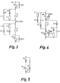
- the controlled diode recovery (C.D.R.) circuit is shown in figure 1 .
- This circuit allows the corresponding power switch (such as switches M1-M4 in Fig. 2) to be turned on rapidly, without regard for the main diode D1 recovery current slope or magnitude.
- the circuit below D1 has the function of controlling the reverse recovery current of D1, while giving low power loss, and unhindered forward conduction of D1.
- L1 is a saturable inductor.
- D1 When the cathode of D1 is pulled high relative to the bottom rail of the circuit, D1 will not block reverse current flow until it recovers. No current will flow through the D3 branch, as it recovers almost immediately, due to no forward current previously flowing through D3. L1, which was previously carrying current from bottom to top, will block the voltage now across it until its volt-second rating is exceeded. Therefore, the only branch which will support reverse recovery current of D1 is presently the L2/D2 branch. The current flow starts at zero and increases approximately nearly due to the voltage across L2.
- L1 When D1 is next required to conduct, L1 will rapidly saturate (if not already saturated) during the fall time of the top rail voltage. Some current flows through D3/Z1, before L1 fully saturates, during the rise time of the forward current through D1. When L1 saturates, it will carry all the forward conduction current, allowing D3 to recover.
- the C.D.R. circuit adds no significant conduction losses, and reduces switching losses due to the controlled reverse recovery current of the main diode.
- the overall power converter is shown in figure 2 .
- the power flow does not have to be from the mains input to the output, but the rms voltage on the terminals shown as output will always be less than or equal to the voltage at the terminals shown as mains input.
- the circuit behaves in a similar way to a forward converter when transferring energy from the mains input to the output, but behaves in a similar way to a flyback converter when transferring energy from the output to the input.
- the novel configuration contains an impedance Z2 to join the two branches.
- the connection to output impedance L out may be taken from either side of Z2.
- Novel circuits to control diode reverse recovery are shown as blocks (C.D.R. Circuit) in figure 2, but are expanded in figure 1.
- the switching devices shown M1-M4 are MOSFETs, but other semiconductor switching devices may be used instead.
- the circuits to generate the gate drives for M1-M4 are not shown.
- C in forms the last stage of the input filter, and L out forms the first stage of the output filter.
- the top switching devices M1 & M3 are turned on to connect the output inductor L out to the input capacitor C in , or alternatively the bottom switches M2 & M4 are turned on to connect L out to ground (neutral), providing a freewheel path.
- This switching between top switches and bottom switches is carried out at a high frequency and a variable duty ratio.
- the duty ratio of top:top+bottom switch on-times scales the average voltage seen by L out at its left terminal. If the duty ratio is left constant, the output waveform will be a scaled version of the input waveform.
- High frequency filters may be used to prevent the switching frequency and its harmonic components from reaching the supply or load. If filtering is not required, the H.F. filters may be replaced with a short circuit from input to output, L out may be replaced by a short circuit, and C in may be replaced by an open circuit.
- the M1-M2 branch carries current only when the current through L out flows from left to right.
- the M3-M4 branch carries current only when the current through L out flows from right to left. Only one switch is required to control current flow for a specific combination of input voltage polarity and output current direction, other switches being left on or off as appropriate.
- the novel a.c. chopper circuit configuration of two branches (M1-M2 and M3-M4 with their associated diode circuits) joined by Z2 allows an overlap of the on-time between the top M1 & M3 and bottom M2 & M4 switches.
- An inductive component of Z2 prevents the large currents which would otherwise flow (if Z2 was a short-circuit) through the effective short-circuit of C in by M1-M4 or M2-M3 during the overlap time. Overlap of the on-times may be caused by timing errors of gate drive signals, rise/fall times of switch currents, or undesirable dv/dt turn-on of switches.
- One possible configuration for Z2 is an inductor and resistor in parallel, the inductor preventing large currents during overlap, and the resistor dissipating the energy stored in the inductor due to overlap of switch on-times.
- the a.c. chopper may be used in light dimmers, power supplies, motor controllers, heating controllers, voltage regulators/stabilisers or other applications requiring an a.c. input voltage to be converted to a higher or lower output voltage.
- the C.D.R. circuit is not restricted to use in an a.c. chopper, but may be used to reduce switching losses and device stresses in any circuit which requires fast recovery diodes. Possible uses are in switching power supplies, light dimmers, motor controllers, heater controllers, electronic ballasts, and other power applications.
- the saturable inductor, L1 has some finite inductance even when saturated. This means some energy is stored when current is flowing, causing a voltage spike across the series switch during turn-off. Provided the saturated inductance is small enough, the energy stored here will (usefully) charge the output capacitance of the switch at turn-off.
- L1 Due to an imperfect hysteresis loop, L1 will allow some reverse current flow through D1, though this will be limited. This current adds to the controlled current slope, and will increase recovery speed but gives larger peak recovery current.
- Figure 3 shows the case when the semiconductor switches M1 and M2 are used in a half- or full-bridge arrangement.
- the switches are connected in series, across a constant polarity supply voltage. Operation can be explained by first assuming steady state starting conditions, such that current is flowing from the load (connected at the junction of the saturable inductors L1 and L3), up through L1 and Dm1 (the body or external diode of M1). M1 drain is connected to the positive supply rail, and M2 source is connected to the negative supply rail. M2 is in the off state.
- L2 As the current through L2 (top branch) decays, it has a positive voltage on its bottom terminal with respect to its top, giving a positive voltage on the bottom terminal of L1 with respect to its top. This shifts the state of L1 towards saturation for current flow from bottom to top.
- the volt-time required to reduce the current flow through L2 (top branch) to zero is the same as that now needed to saturate L1.
- FIG. 4 shows the circuit diagram for the case when using two semiconductor switches M1, M2 (shown as MOSFETs in the diagram) connected in an anti-series configuration for a.c. switching.
- L1 is a square loop saturable inductor connected between the switches.
- the body diode Dm1, Dm2 of each switch has its recovery circuit connected in parallel with the series combination of the saturable inductor L1 and the other of the switches M2, M1.
- Each recovery circuit includes a series connection of diode D2 and inductor L2.
- Diode D2 has its forward direction opposite to the diode it controls the recovery of (Dm1 or Dm2).
- diode D3 In each recovery circuit branch there is also a series combination of a further diode D3 and impedance Z1 shunting the inductor L2.
- the diode D3 has its forward direction opposite to the forward direction of D2.
- M1 is turned off, and the top rail (M1 drain) is pulled high (externally) with respect to the bottom rail (M2 drain) and the circuit here is required to go into a blocking state. Since Dm1 was carrying forward current, it will not block until after its reverse recovery time. Dm2 is biased for forward conduction, so will not block. L1 was previously carrying current from bottom to top, so it is saturated for current flow in this direction, but will block the positive voltage now on its top terminal. D2 at left branch and D3 at right branch were not previously carrying current, so they will block almost immediately, leaving only L2/D2 of the right branch to carry the reverse recovery current of Dm1.
- L2 of the right branch will allow a controlled rate of increase in reverse recovery current, and when Dm1 recovers, the peak recovery current now flowing in L2 of the right branch will freewheel through Z1/D3 of the right branch.
- the current through L2 of the right branch decays, it has a positive voltage on its bottom terminal with respect to its top, giving a positive voltage on the bottom terminal of L1 with respect to its top. This shifts the state of L1 towards saturation for current flow from bottom to top.
- the volt-time required to reduce the current through L2 of the right branch to zero is the same as that now needed to saturate L1.
- the circuit is now in a blocking state, due to Dm1, but ready for conduction from bottom to top, due to L1 being saturated for current flow in this direction. This means that if the top rail (M1 drain) is pulled low with respect to the bottom rail, then current will flow through M2, L1 and Dm1 as in the original state.
- the circuit is symmetrical, so operation is identical when the voltage polarity across the rails is reversed, and the current flow is in the opposite direction, the symmetrically placed components being used instead of those described above.
- circuit configurations which are covered by the same inventive concept. Such configurations are:
Landscapes
- Engineering & Computer Science (AREA)
- Power Engineering (AREA)
- Dc-Dc Converters (AREA)
- Electronic Switches (AREA)
Priority Applications (1)
| Application Number | Priority Date | Filing Date | Title |
|---|---|---|---|
| EP02010727A EP1237270A3 (fr) | 1998-02-05 | 1998-08-25 | Circuit de récupération commandé pour diode |
Applications Claiming Priority (4)
| Application Number | Priority Date | Filing Date | Title |
|---|---|---|---|
| FI973783 | 1997-09-25 | ||
| FI973783A FI114354B (fi) | 1997-09-25 | 1997-09-25 | Piiri diodin hallittua elpymistä varten |
| FI980259A FI113915B (fi) | 1997-09-25 | 1998-02-05 | Piiri runkodiodin hallittua elpymistä varten |
| FI980259 | 1998-02-05 |
Related Child Applications (1)
| Application Number | Title | Priority Date | Filing Date |
|---|---|---|---|
| EP02010727A Division EP1237270A3 (fr) | 1998-02-05 | 1998-08-25 | Circuit de récupération commandé pour diode |
Publications (3)
| Publication Number | Publication Date |
|---|---|
| EP0905873A2 true EP0905873A2 (fr) | 1999-03-31 |
| EP0905873A3 EP0905873A3 (fr) | 2000-05-10 |
| EP0905873B1 EP0905873B1 (fr) | 2002-11-06 |
Family
ID=26160445
Family Applications (1)
| Application Number | Title | Priority Date | Filing Date |
|---|---|---|---|
| EP98202840A Expired - Lifetime EP0905873B1 (fr) | 1997-09-25 | 1998-08-25 | Circuit de récupération commandé pour diode ou diode de corps |
Country Status (3)
| Country | Link |
|---|---|
| EP (1) | EP0905873B1 (fr) |
| DE (1) | DE69809169T2 (fr) |
| FI (1) | FI113915B (fr) |
Cited By (3)
| Publication number | Priority date | Publication date | Assignee | Title |
|---|---|---|---|---|
| EP1052774A3 (fr) * | 1999-04-16 | 2002-02-06 | Patent-Treuhand-Gesellschaft für elektrische Glühlampen mbH | Circuit avec un démipont |
| GB2533965A (en) * | 2015-01-09 | 2016-07-13 | Allan Macfarlane Alistair | Improved AC supply voltage, current and power factor regulator |
| EP4002669A1 (fr) * | 2019-11-21 | 2022-05-25 | Turbo Power Systems Ltd | Améliorations des réseaux de distribution d'électricité |
Family Cites Families (5)
| Publication number | Priority date | Publication date | Assignee | Title |
|---|---|---|---|---|
| GB2045549B (en) * | 1979-03-06 | 1982-12-15 | Gould Advance Ltd | Power regulating apparatus |
| GB8816774D0 (en) * | 1988-07-14 | 1988-08-17 | Bsr Int Plc | Power supplies |
| US5202820A (en) * | 1991-12-16 | 1993-04-13 | Ford Motor Company | Saturable inductor protection circuit for inductive load driver |
| GB2301239B (en) * | 1995-05-24 | 1999-12-01 | Stephen Soar | Electric converter |
| JPH09103073A (ja) * | 1995-10-05 | 1997-04-15 | Fujitsu Denso Ltd | Dc−dcコンバータ |
-
1998
- 1998-02-05 FI FI980259A patent/FI113915B/fi not_active IP Right Cessation
- 1998-08-25 DE DE69809169T patent/DE69809169T2/de not_active Expired - Fee Related
- 1998-08-25 EP EP98202840A patent/EP0905873B1/fr not_active Expired - Lifetime
Cited By (4)
| Publication number | Priority date | Publication date | Assignee | Title |
|---|---|---|---|---|
| EP1052774A3 (fr) * | 1999-04-16 | 2002-02-06 | Patent-Treuhand-Gesellschaft für elektrische Glühlampen mbH | Circuit avec un démipont |
| GB2533965A (en) * | 2015-01-09 | 2016-07-13 | Allan Macfarlane Alistair | Improved AC supply voltage, current and power factor regulator |
| GB2533965B (en) * | 2015-01-09 | 2021-12-22 | Allan Macfarlane Alistair | Improved switched-mode AC voltage, current and power factor regulator |
| EP4002669A1 (fr) * | 2019-11-21 | 2022-05-25 | Turbo Power Systems Ltd | Améliorations des réseaux de distribution d'électricité |
Also Published As
| Publication number | Publication date |
|---|---|
| DE69809169D1 (de) | 2002-12-12 |
| EP0905873B1 (fr) | 2002-11-06 |
| FI980259A7 (fi) | 1999-03-26 |
| DE69809169T2 (de) | 2003-10-02 |
| EP0905873A3 (fr) | 2000-05-10 |
| FI980259A0 (fi) | 1998-02-05 |
| FI113915B (fi) | 2004-06-30 |
Similar Documents
| Publication | Publication Date | Title |
|---|---|---|
| CA2489345C (fr) | Convertisseur de puissance a source d'impedance | |
| US4933831A (en) | Power supply | |
| CA2271792C (fr) | Amortisseurs de verrou de tension a verrouillage au point neutre (npc) pour des convertisseurs a trois niveaux | |
| JP2636918B2 (ja) | 疑似共振電流モード静止電力変換方法及び装置 | |
| US5936855A (en) | Harmonic correction of 3-phase rectifiers and converters | |
| US5471376A (en) | Low-loss active voltage-clamp circuit for single-ended forward PWM converter | |
| EP2858195B1 (fr) | Circuit de convertisseur | |
| EP0440245B1 (fr) | Circuit d'alimentation | |
| US5642273A (en) | Resonant snubber inverter | |
| EP0698961A2 (fr) | Circuit limiteur à pertes faibles | |
| US7184287B2 (en) | Rectifier clamping circuit with reverse energy recovery | |
| CN1301821C (zh) | 带有缓冲电路的电源 | |
| US10848071B2 (en) | Highly reliable and compact universal power converter | |
| EP0336952A4 (fr) | Contivertisseur de puissance de courant continu en courant continu. | |
| US7688044B2 (en) | Device for transforming and stabilizing a primary AC voltage for supplying an electric load | |
| EP0905873B1 (fr) | Circuit de récupération commandé pour diode ou diode de corps | |
| EP0905871A2 (fr) | Convertisseur de puissance courant alternatif - courant alternatif à fréquence de ligne | |
| KR101256032B1 (ko) | 솔리드 스테이트 스위칭 회로 | |
| WO1994014230A1 (fr) | Convertisseur auto-oscillant a inductance serie comprenant une bobine d'inductance oscillante en trois parties | |
| CN1091972C (zh) | 一种软开关脉宽调制电路 | |
| EP1237270A2 (fr) | Circuit de récupération commandé pour diode | |
| KR20200118932A (ko) | 고속 스위칭 인버터 | |
| SU1089736A1 (ru) | Трехфазный преобразователь переменного напр жени в переменное (его варианты) | |
| CA2051668A1 (fr) | Circuits a commutation protegee et pieces connexes | |
| JPH0270267A (ja) | 並列形共振コンバータ |
Legal Events
| Date | Code | Title | Description |
|---|---|---|---|
| PUAI | Public reference made under article 153(3) epc to a published international application that has entered the european phase |
Free format text: ORIGINAL CODE: 0009012 |
|
| AK | Designated contracting states |
Kind code of ref document: A2 Designated state(s): DE FR GB IT NL |
|
| AX | Request for extension of the european patent |
Free format text: AL;LT;LV;MK;RO;SI |
|
| RIC1 | Information provided on ipc code assigned before grant |
Free format text: 6H 03K 17/0814 A |
|
| RAP1 | Party data changed (applicant data changed or rights of an application transferred) |
Owner name: HELVAR OY AB |
|
| PUAL | Search report despatched |
Free format text: ORIGINAL CODE: 0009013 |
|
| RIC1 | Information provided on ipc code assigned before grant |
Free format text: 7H 03K 17/0814 A, 7H 02M 5/293 B |
|
| AK | Designated contracting states |
Kind code of ref document: A3 Designated state(s): AT BE CH CY DE DK ES FI FR GB GR IE IT LI LU MC NL PT SE |
|
| AX | Request for extension of the european patent |
Free format text: AL;LT;LV;MK;RO;SI |
|
| 17P | Request for examination filed |
Effective date: 20001110 |
|
| AKX | Designation fees paid |
Free format text: DE FR GB IT NL |
|
| 17Q | First examination report despatched |
Effective date: 20010306 |
|
| GRAG | Despatch of communication of intention to grant |
Free format text: ORIGINAL CODE: EPIDOS AGRA |
|
| GRAG | Despatch of communication of intention to grant |
Free format text: ORIGINAL CODE: EPIDOS AGRA |
|
| GRAH | Despatch of communication of intention to grant a patent |
Free format text: ORIGINAL CODE: EPIDOS IGRA |
|
| GRAH | Despatch of communication of intention to grant a patent |
Free format text: ORIGINAL CODE: EPIDOS IGRA |
|
| GRAA | (expected) grant |
Free format text: ORIGINAL CODE: 0009210 |
|
| AK | Designated contracting states |
Kind code of ref document: B1 Designated state(s): DE FR GB IT NL |
|
| PG25 | Lapsed in a contracting state [announced via postgrant information from national office to epo] |
Ref country code: NL Free format text: LAPSE BECAUSE OF FAILURE TO SUBMIT A TRANSLATION OF THE DESCRIPTION OR TO PAY THE FEE WITHIN THE PRESCRIBED TIME-LIMIT Effective date: 20021106 Ref country code: IT Free format text: LAPSE BECAUSE OF FAILURE TO SUBMIT A TRANSLATION OF THE DESCRIPTION OR TO PAY THE FEE WITHIN THE PRESCRIBED TIME-LIMIT;WARNING: LAPSES OF ITALIAN PATENTS WITH EFFECTIVE DATE BEFORE 2007 MAY HAVE OCCURRED AT ANY TIME BEFORE 2007. THE CORRECT EFFECTIVE DATE MAY BE DIFFERENT FROM THE ONE RECORDED. Effective date: 20021106 Ref country code: FR Free format text: LAPSE BECAUSE OF FAILURE TO SUBMIT A TRANSLATION OF THE DESCRIPTION OR TO PAY THE FEE WITHIN THE PRESCRIBED TIME-LIMIT Effective date: 20021106 |
|
| REG | Reference to a national code |
Ref country code: GB Ref legal event code: FG4D |
|
| REF | Corresponds to: |
Ref document number: 69809169 Country of ref document: DE Date of ref document: 20021212 |
|
| NLV1 | Nl: lapsed or annulled due to failure to fulfill the requirements of art. 29p and 29m of the patents act | ||
| EN | Fr: translation not filed | ||
| PLBE | No opposition filed within time limit |
Free format text: ORIGINAL CODE: 0009261 |
|
| STAA | Information on the status of an ep patent application or granted ep patent |
Free format text: STATUS: NO OPPOSITION FILED WITHIN TIME LIMIT |
|
| 26N | No opposition filed |
Effective date: 20030807 |
|
| PGFP | Annual fee paid to national office [announced via postgrant information from national office to epo] |
Ref country code: GB Payment date: 20040712 Year of fee payment: 7 |
|
| PGFP | Annual fee paid to national office [announced via postgrant information from national office to epo] |
Ref country code: DE Payment date: 20040716 Year of fee payment: 7 |
|
| PG25 | Lapsed in a contracting state [announced via postgrant information from national office to epo] |
Ref country code: GB Free format text: LAPSE BECAUSE OF NON-PAYMENT OF DUE FEES Effective date: 20050825 |
|
| PG25 | Lapsed in a contracting state [announced via postgrant information from national office to epo] |
Ref country code: DE Free format text: LAPSE BECAUSE OF NON-PAYMENT OF DUE FEES Effective date: 20060301 |
|
| GBPC | Gb: european patent ceased through non-payment of renewal fee |
Effective date: 20050825 |