EP0905941A1 - Circuit de synchronisation de trames - Google Patents
Circuit de synchronisation de trames Download PDFInfo
- Publication number
- EP0905941A1 EP0905941A1 EP98902191A EP98902191A EP0905941A1 EP 0905941 A1 EP0905941 A1 EP 0905941A1 EP 98902191 A EP98902191 A EP 98902191A EP 98902191 A EP98902191 A EP 98902191A EP 0905941 A1 EP0905941 A1 EP 0905941A1
- Authority
- EP
- European Patent Office
- Prior art keywords
- frame
- data
- period
- start position
- length
- Prior art date
- Legal status (The legal status is an assumption and is not a legal conclusion. Google has not performed a legal analysis and makes no representation as to the accuracy of the status listed.)
- Granted
Links
Images


Classifications
-
- H—ELECTRICITY
- H04—ELECTRIC COMMUNICATION TECHNIQUE
- H04L—TRANSMISSION OF DIGITAL INFORMATION, e.g. TELEGRAPHIC COMMUNICATION
- H04L7/00—Arrangements for synchronising receiver with transmitter
- H04L7/02—Speed or phase control by the received code signals, the signals containing no special synchronisation information
-
- H—ELECTRICITY
- H04—ELECTRIC COMMUNICATION TECHNIQUE
- H04J—MULTIPLEX COMMUNICATION
- H04J3/00—Time-division multiplex systems
- H04J3/02—Details
- H04J3/06—Synchronising arrangements
- H04J3/0602—Systems characterised by the synchronising information used
- H04J3/0605—Special codes used as synchronising signal
- H04J3/0608—Detectors therefor, e.g. correlators, state machines
-
- H—ELECTRICITY
- H04—ELECTRIC COMMUNICATION TECHNIQUE
- H04L—TRANSMISSION OF DIGITAL INFORMATION, e.g. TELEGRAPHIC COMMUNICATION
- H04L7/00—Arrangements for synchronising receiver with transmitter
- H04L7/04—Speed or phase control by synchronisation signals
- H04L7/08—Speed or phase control by synchronisation signals the synchronisation signals recurring cyclically
Definitions
- the present invention relates to a frame synchronization circuit suitable to transmit data sequence which have a frame composition in the environment where a code error, especially a data loss or data insertion in units of cells or packets, is prone to generate.
- a method for adding a unique word such as M sequence to each frame as a frame synchronization code has been widely used on its transmitting side.
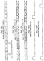
- the position to which the unique word is added is not particularly defined in this method, but in general, the unique word is set to the head of a frame to simplify the composition, as shown in FIG. 1A.
- the unique word in the received data sequence is detected on the reception side, so that the frame position is identified to detect each frame and a transmission information data is reproduced from the each frame detected.
- FIGs. 1B and 1C An example of such frame composition concerning this technique is shown in FIGs. 1B and 1C. These figures show arrangements of identical unique words. That is, FIG. 1C displays an information data for every block of predetermined length (M + 1 bits) and FIG. 1B expands the information data for every one bit.
- unique words are constituted of the most significant bit (bits S1 to SN) of each block, and the signal shown in FIG. 1B can he obtained by expanding the unique words to a serial data from high order bit sequentially.
- the intervals assigned may be nonuniform and also plural bits may be assigned.
- M and N are natural numbers.
- a frame length information can also be used in addition to the unique word as a frame synchronization code, as shown in FIG. 1D.
- An appearance position of the following frame synchronization code can be known on the reception side by using the frame length information, so that the probability of occurring the out of detection or false detection of the frame synchronization code can be reduced compared with the case in which only the unique word is used.
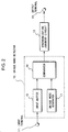
- FIG. 2 shows a composition of a conventional frame synchronization circuit (Example 1).
- the frame synchronization circuit shown in FIG. 2 is premised to be applied to a transmission system of a fixed length frame.
- a received data sequence input from an input terminal 11 is sent to a unique word detector 12.
- an input buffer 15 buffers the received data sequence sent from the input terminal 11, cuts out data equivalent to the unique word length at every predetermined timing to supply the data to a comparator 16, and then shifts a cut out position of the data by one bit at every same timing.
- the comparator 16 compares the data supplied from the input buffer 15 and the unique word given from a unique word generator 17, and supplies "1" when the data is in accordance with the unique word or "0" when both are in disagreement to a synchronization judgment circuit 13 as a comparison result. In this case, in order to prevent the out of detection based on code error occurred when comparison operation is performed in the comparator 16, the disagreement of the number of constant bits may be permitted to provide "agreement".
- FIG. 3 is a state transition chart of the synchronisation judgment circuit 13.
- the synchronization judgment circuit 13 is, at first, in an out of synchronization state S1 in which frame synchronization is not established at all.
- the synchronization judgment circuit 13 in the out of synchronization state S1 transfers its own state to a backward 1 state S2 as "detection", when "1" is supplied from the comparator 16, and holds its own state in the out of synchronization state S1 as "out of detection", when "0" is supplied.
- the synchronization judgment circuit 13 transferred to the backward 1 state S1 skips the received data sequence by the fixed frame length to wait for the output of the comparator 16.
- the synchronization judgment circuit 13 transfers its own state to a next backward 2 state S3 as “detection”, and when it is "0", returns back to the out of synchronization state S1 as "out of detection”.
- the processing similar to that described above is also performed in states after the backward 2, and the state of the synchronization judgment circuit 13 returns immediately back to the out of synchronization state S1 in the case of out of detection, and advances toward a synchronization establishment state S5 when "detection" continues for total of N+1 times.
- the states from the backward 1 to the backward N are set to reduce occurrence frequency of false synchronization, and generally, such setting is called as "backward protection".
- backward protection When the backward protection is not set up, if the part which agrees with a unique word accidentally exists somewhere in the part other than the unique word in the received data sequence, a false detection which detects the unique word by mistake may occur, resulting in frequent false synchronization.
- the synchronization judgment circuit 13 illustrated in the present invention is provided with a backward protection and also repeats agreement judgment for N+1 times to reduce the occurrence frequency of the false synchronization due to false detection.
- the synchronization judgment circuit 13 even when in the synchronization establishment state S5, skips the received data sequence only by the fixed frame length to wait an output from the comparator 16.
- the synchronization judgment circuit 13 retains its own state in the synchronization establishment state S5 as “detection”, and when "0" is supplied, transfers its own state to a forward 1 state S6 as "out of detection".
- the processes in the states from the forward 1 to a forward M are contrary to those in the states from the backward 1 to the backward N described above, and in the case of "detection", the process returns immediately to the synchronization establishment state S5, and when "out of detection" continues for total of M+1 times, the process returns back to the out of synchronization state S1.
- the states from the forward 1 to the forward M are provided in order to avoid frequent occurrence of "synchronous error”, and such setting is generally called as "forward protection".
- forward protection When the forward protection is not provided, the synchronization may be come out immediately when the out of detection due to code error occurs.
- the synchronization judgment circuit 13 illustrated in the example is provided with the forward protection and repeats the agreement judgment for M+1 times to reduce the occurrence frequency of the "synchronous error".
- the synchronization can also be established using a circuit of the similar composition as Example 1 shown in FIG. 2, except the function and operation of the synchronization judgment 13.
- the appearance position of the following frame synchronization code can not be forecasted in advance on the reception side, so that the synchronization can not be established stably by performing the state transfer shown in FIG. 3, and the unique words have to be detected by shifting a received data sequence by one bit sequentially for all frames. For this reason, the trial frequency of the unique word detection will be increased, resulting in higher occurrence frequency of false detection. Therefore, in the example, the composition and operation of the frame synchronization circuit will be described in which not only the unique word but also the frame length information are used as the frame synchronization code.
- FIG. 4 shows a composition of a conventional frame synchronization circuit (Example 2) using the unique word and frame length information as the frame synchronization code.
- Example 2 the common parts to each part of FIG. 2 are identified by the same reference character and their explanations will be omitted.
- the differences between Example 2 shown in FIG. 4 and Example 1 shown in FIG. 2 are such that the synchronization judgment circuit 13 is replaced with a synchronization circuit 13a and a frame length information detector 18 is newly provided.
- the frame length information detector 18 extracts the frame length information followed by the unique word according to the received data sequence input from the input terminal 11 and a frame synchronization output supplied from the synchronization judgment circuit 13a to the output terminal 14, and supplies an output data to the synchronization judgment circuit 13a after decoding is performed.
- the synchronization judgment for the received data sequence may be affected, so that the error correction and detection process (coding and decoding) is often provided to the frame length information in order to improve the reliability of the frame length information.
- the synchronization judgment circuit 13a presumes a position of the following frame synchronization code using the frame length information supplied from the frame length information detector 18 when detecting the frame synchronization code, and skips over the received data sequence to the presumed position concerned to wait for the output of the comparator 16.
- the operation except having described above is as similar to that of Example 1, therefore, the synchronization judgment according to the state transfer shown in FIG. 3 can be performed as with the fixed length frame, allowing the establishment of the stable synchronization.
- Example 3 a conventional frame synchronization circuit (Example 3) will be explained in which the synchronization judgment is achieved without following the state transfer shown in FIG. 3.
- the unique word and frame length information are used as the frame synchronization codes, and the error correction and detection processes are premised to be applied to the frame length information.
- the frame length information without error is detected in a position followed by the unique word, it is judged that a correct frame synchronization code has been detected.
- the occurrence frequency of false detection can be more reduced than if only the unique word is used as the frame synchronization code, so that the frame synchronization position can be judged with high reliability without adopting the state transfer shown in FIG. 3.
- the conventional frame synchronization circuit for a fixed and variable length frames operate effectively in either case for a typical code error, such as a random error and burst error, in a conventional transmission system.
- FIGs. 5A to 5D there is shown an example of data loss/insertion in FIGs. 5A to 5D.
- a data loss packet loss
- FIG. 5A when a data loss (packet loss) occurs in a received data sequence FIG. 5A, the length of the frame in which data loss has occurred is made shorter than an original frame length 5B.
- data insertion packet insertion
- the length of the frame in which data insertion has occurred is made longer than the original frame length 5D.
- the frame synchronization circuit (Example 3) which does not use the state transfer of FIG. 3 in a data transmission system using variable length frames, although the continuous synchronous error described above does not occur, frames which are shorter or longer than those expressed with the frame length information included in the frame synchronization code are received, so that the following frame synchronization position can not be detected correctly, thereby the synchronization codes can not be detected not only in frames in which the data loss/insertion has occurred but also in frames followed by the frames, resulting in synchronous error of at least total of two frames.
- the present invention has been made in an attempt to solve the above-described problems, and therefore, has a first object to provide a frame synchronization circuit which can prevent the occurrence of synchronous error due to data loss/insertion while restraining the false synchronization/out of synchronization according to the typical code error, such as random error and burst error, in a conventional transmission system.
- a frame synchronization circuit used on the reception side of a data transmission system adopting a frame composition positioning a frame synchronization code scatteredly in a frame is characterized by comprising:
- a dummy data insertion and deletion circuit is added to the above described composition which outputs a corrected received data sequence produced by inserting a dummy data into the presumed data loss period and deleting data from the presumed data insertion period for said received data sequence.
- said first frame synchronization code detector and said second frame synchronization code detector use frame synchronization positions output from said synchronization judgment circuit as initial values, when a data loss period or a data insertion period is presumed by said data loss and data insertion period judgment circuit.
- said data loss and data insertion period judgment circuit when said frame length information of a frame to be processed is different from a length output from said difference circuit, judges provisionally that a data loss has occurred in the frame,
- a frame number is used together, and in addition to said (1) and (2), when said first start position is prior to said second start position on time axis and a frame number showed by said first frame position is continuous with an immediately following frame number showed by said second frame position, it is judged finally that a data loss of said number of bits has occurred in any position in the period from said first start position to said second start position, and only when a case is not applicable to this, a process is made to be advanced after said (3) for the first time, furthermore, in addition to said (3) and (4), when a length of an period from said first start position to said second start position is longer than a length output from said difference circuit, it is judged finally that a data insertion of said number of bits has occurred in any position in the period.
- a first and second threshold values are introduced, and when said frame length information of a frame to be processed is different from a length output from said difference circuit and the difference of the both is shorter than a predetermined first threshold value, said data loss and data insertion period judgment circuit judges provisionally that a data loss has occurred in the frame, and in addition to said (1) and (2), when said first start position is prior to said second start position on time axis, it is judged finally that a data loss of said number of bits has occurred in any position in the period from said first start position to said second start position, when said frame length information of said frame is different from a length output from said difference circuit and also the length output from said difference circuit is shorter than a predetermined second threshold value, it is judged provisionally that a data insertion has occurred in the frame, and in addition to said (3) and (4), when a length of an period from said first start position to said second start position is longer than a length output from said difference circuit, it is judged finally that a data insertion of said number of bits has
- a frame synchronous error does not come out and also the position and length of the data loss and data insertion can be presumed correctly.
- an information data with correct length can be reproduced by inserting a dummy data into the period judged to be a data loss period and by deleting the data of the period concerned from the period judged to be a data insertion period.
- a data loss in packet units can be transformed into a burst error, and even if a data insertion may occur, the effect resulted from this can be removed completely in an ideal case.
- this embodiment can be applied not only to a fixed length frame but also to a variable length frame.
- this embodiment can be applied not only to a fixed length frame but also to a variable length frame.
- the present embodiment is based on the composition corresponding to a frame synchronization circuit concerned with claim 1 and the function corresponding to a frame synchronization circuit concerned with claim 4, so that thereafter the explanation will be advanced based on this basic composition and function.
- the explanation will be added to embodiments with distinctive composition of frame synchronization circuits concerned with other claims to clarify the relations to each claim.
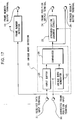
- FIG. 8 is a block diagram showing a composition (Composition 1) of a frame synchronization circuit according to an embodiment of the present invention.
- 31 is an input terminal into which a received data sequence is input
- 32 is a first synchronization code detector which checks the received data sequence input from the input terminal 31 and a unique word produced inside of the frame synchronization circuit on time axis in the forward direction and outputs a first checked result 40 and a first frame position 37 which is a synchronization position candidate based on the checked result concerned.
- symbol 33 designates a second synchronization code detector which checks the received data sequence input from the input terminal 31 and a unique word produced inside of the frame synchronization circuit on time axis in the backward direction and outputs a second checked result 41 and a second frame position 38 which is a synchronization position candidate based on the checked result concerned.
- checking on time axis in the forward direction is referred to as a processing which views the received data sequence in the order of reception and also views the reference unique word in the order corresponding to this sequence to compare for every corresponding bit.
- checking on time axis in the backward direction is referred to as a processing which views the received data sequence in the opposite order of reception and also views the reference unique word in the order corresponding to this opposite sequence to compare for every corresponding bit.
- Symbol 44 designates a difference circuit which outputs the difference between the first frame position 37 and the second frame position 38
- 34 is a data loss and data insertion period judgment circuit which presumes a data loss/insertion period according to the first frame position 37, the second frame position 38, and the output of the difference circuit 44 and outputs the determined period as a judgment result 39
- 35 is a synchronization judgment circuit which decides a frame synchronization position based on the first frame position 37, the second frame position 38, and the judgment result 39 to output it to a frame position output terminal 36.
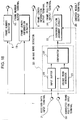
- FIG. 9 is a block diagram showing a composition (Composition 2) of a modification of a frame synchronization circuit according to another embodiment of the present invention. What is greatly different between the frame synchronization circuit shown in this Figure and the one shown in FIG. 8 is to provide a dummy data insertion and deletion circuit 42.
- the dummy data insertion and deletion circuit 42 corrects the received data sequence input from the input terminal 31 according to the output from the data loss and data insertion period judgment circuit 34 and outputs the received data sequence corrected (corrected received data sequence) through a corrected received data sequence output terminal 43.
- the concrete correction processing will be described hereinafter in an explanation of the operation. A-3. Composition where broken line parts are added to FIGs. 8 and 9
- compositions (Compositions 3, 4) of modification of each frame synchronization circuit are shown in FIGs. 8 and 9 by expressing additional portions with broken lines.
- FIG. 6 is a schematic view showing one example of the received data sequence in this embodiment.
- a frame synchronization code is positioned in a frame scatteredly in the present invention.
- a frame length is defined as a fixed length
- a frame synchronization code is made a unique word such as M sequence
- a method for scattered positioning is an equal interval positioning of single bits (total of N bits) at intervals of M bits. Therefore, the frame length becomes N x (M + 1) bits and the information data length becomes N x M bits.
- N and M are natural numbers.
- FIG. 6 illustrates the composition of the i-th frame (i is a natural number) of a received data sequence.
- the first bit S1 of a frame synchronization code is arranged, subsequently M-bit information data, the second bit S2, M-bit information data, ... , the N-th bit SN, and M-bit information data are arranged.
- the frame synchronization is not affected, so that a fixed length frame of arbitrary length can actually processed.
- FIGs. 7A to 7H shows only a part of frame synchronization code extracted from a received data sequence illustrated in FIG. 6.
- FIG. 7A a received data sequence without code error
- FIG. 7C a received data sequence in which code errors have occurred in positions marked "x" in the figure
- FIG. 7C obtained when frame synchronization is performed in the forward direction on time axis to the received data sequence
- FIG. 7D reference unique words
- FIG. 7E between the received data sequence FIG. 7B and the reference unique words in the forward direction
- FIG. 7F obtained when frame synchronization is performed in the backward direction on time axis to the received data sequence FIG. 7B, reference unique words FIG. 7G in the opposite direction on time axis, and a checked result (a second checked result) FIG. 7H between the received data sequence FIG. 7B and the reference unique words in the backward direction.
- the code errors have occurred at the fourth bit S4 and sixth bit S6.
- the first frame positions obtained by frame synchronization detection in the forward direction on time axis agrees with the second frame positions obtained by frame synchronization detection in the backward direction on time axis, and both designates the normal positions. Therefore, the output of the difference circuit 44 agrees with the length of the frame to be detected.
- the first frame position shows the head position of the frame to be processed (detected) and the second frame position indicates the head position of the immediately following frame of the frame concerned.
- plural of "1" indicating the disagreement of check occur in the fourth bit S4 and sixth bit S6, but the both checked results are agreed completely.
- the frame synchronization circuit according to the present embodiment operates like a conventional frame synchronization circuit.
- the similar operation is also performed in the above described Composition 2 to 4.
- the dummy data insertion and deletion circuit 42 makes the received data sequence pass through to the corrected received data sequence output terminal 43.
- the data loss and data insertion period judgment circuit 34 outputs nothing, the first frame synchronization code detector 32 and second frame synchronization code detector are not initialized.
- FIGs. 10A to 10M shows only a portion of a frame synchronization code extracted from the received data sequence illustrated in FIG. 6.
- a received data sequence FIG. 10A without code error a received data sequence FIG. 10B in which data loss has occurred in a frame
- the first frame position FIG. 10C in the forward direction to the received data sequence FIG. 10B reference unique words FIG. 10D in the forward direction on time axis
- the second frame position FIG. 10F in the backward direction to the received data sequence FIG. 10B reference unique words FIG. 10G in the backward direction on time axis
- the second checked result FIG. 10H in the backward direction to the received data sequence FIG. 10B.
- four bits from the fifth bit S5 to eighth bit S8 are lost due to data loss.
- the received data sequence concerned is supplied to the first frame synchronization code detector 32 and the second frame synchronization code detector 33.
- an inner composition example (Inner composition example 1) of each frame synchronization code detector is shown in FIG. 12.
- the inner composition example 1 shown in this figure is composed of a reception data input terminal 21, a unique word detector 22 which compares the received data sequence from the reception data input terminal 21 and the reference unique word to output the compared result, a synchronization judgment circuit 23 which detects a frame position based on the compared result concerned, a frame position output terminal 24 which outputs the detected frame position, and a checked result output terminal 29 which outputs the compared result of the unique word detector 22.
- the unique word detector 22 is provided with an input buffer 25 which buffers a received data sequence from the reception data input terminal 21 to output a candidate of unique data, a unique word generator 27 which generates a reference unique word, and a comparator 26 which compares both to output a compared result (for example, exclusive OR).
- the input buffer 25 cuts out data equal to the unique word length from the data buffered at every predetermined timing to supply it to the comparator 26 and also shifts a cutting out position of data by one bit sequentially at every same timing.
- the data output sequence (bit output sequence) from the input buffer 25 and the unique word generator 27 is in the forward direction on time axis (FIFO) in the first frame synchronization code detector or in the opposite direction on time axis (LIFO) in the second frame synchronization code detector, so that it is necessary to adopt a different composition for each unique word generator, but to avoid the explanation to become complicated in this embodiment, the composition shown in FIG. 12 is made a representative example. Also, in FIGs. 10A to 10M, in order to make the comparison of each data comprehensible, the data in the opposite direction on time axis is transformed into data in the forward direction on time axis.
- the first frame synchronization code detector 32 of the above mentioned composition detects the frame synchronization code from the received data sequence supplied in the forward direction on time axis to output the first frame position 37 shown in FIG. 10C.
- the unique word generator 27 inside of the first frame synchronization code detector 32 generates the reference unique word in the forward direction shown in FIG. 10D, and the first checked result 40 shown in FIG. 10E is generated by checking the reference unique word and the received data sequence.
- the second frame synchronization code detector 33 performs the similar operation as the first frame synchronization code detector 32 described above except detecting the frame synchronization code in the opposite direction on time axis. Therefore, the second frame position 38, the reference unique word in the opposite direction, and the second checked result 41, as shown in FIGs. 10F to 10H, can be obtained. In the example in FIG. 10, code error other than data loss has not occurred, thereby the second checked result FIG.
- M sequence with low autocorrelation or the like is used for a unique word, so that it is rare that the comparison result between the j-th bit Sj and the (j-4)-th bit Sj-4 becomes "in agreement" continuously. That is, it is rare that the first checked result 40 after a data loss occurrence position is set to "0" continuously and the second checked result 41 before the data loss occurrence position is also set “0" continuously.
- the first checked result 40 before the data loss occurrence position and the second checked result 41 after the data loss occurrence position are surely set to "0" when there is no code errors other than data loss.
- the present embodiment using such a characteristic, presumes the data loss occurrence position by using a boundary point at which the first and second checked results become "in disagreement".
- a first checked result example (1) shown in FIG. 10I and a second checked result example (1) shown in FIG. 10J are obtained by assuming that S4 is not equal to S8 and S5 is not equal to S9, and the first start position (immediately after the fourth bit S4) from which there starts a check disagreement subsequent to a check agreement period longer than a predetermined length viewed the first checked result example (1) in the forward direction on time axis agrees with the second start position (immediately before the ninth bit S9) from which there starts a check disagreement subsequent to a check agreement period longer than a predetermined length viewed the second checked result example (1) in the backward direction on time axis.
- the presumed loss length can be obtained by calculating the difference between the frame length information (N) and the output (N-4) of the difference circuit 44.
- the received data sequence with correct length can be reproduced by inserting the lost frame synchronization code and/or information data to the period equal to four bits from the fifth bit S5 to the eighth bit S8.
- it is actually impossible to reproduce the contents of the lost information data correctly on the reception side so that in the present embodiment, when the lost data are information data, dummy data with the same length as that of the lost data are inserted into the period concerned.
- the processing of inserting the lost frame synchronization code and/or dummy data is performed by a dummy data insertion and deletion circuit 42 in Composition 2 and 4 (refer to FIG. 9).
- FIGs. 11A to 11M show only a part of the frame synchronization code extracted from the received data sequence illustrated in FIG. 6, and FIG. 11A to 11H identical with those of FIGs. 10A to 10M are shown in the upper part of FIGs. 11A to 11P. However, FIGs. 11L to 11P are shown in the lower part of the figure in place of FIG. 10I to 10K.
- both of the first start position and the second start position described above exceed the actual data loss positions by one bit, so that the position between the position immediately after the fifth bit S5 and the one immediately before the fourth bit S4 is judged as a presumption loss position. That is, the ambiguity equivalent to two bits occurs in the presumption loss position.
- the presumed loss length is four bits and the presumed loss position is immediately after one of the third bit S3, the fourth bit S4, and the fifth bit S5, so that the received data sequence with correct length is reproduced by inserting the lost frame synchronization code and/or dummy data into the period equal to six bits from the fourth bit S4 to the ninth bit S9, as shown by hatching in FIG. 10N.
- the position at which the checked result becomes "1" for the first time beyond the actual data loss occurrence position changes depending on the autocorrelation of unique word.
- the probability in which the first start position described above agrees with the second start position becomes 25%.
- the probability in which ambiguity of several bits may occur is as follows;
- the data loss period can be presumed with the probability of 80% or more.
- Composition 1 is not provided with the data insertion and deletion circuit, even when a data loss period is turned out, it does not operate the received data. Therefore, it only outputs alarm of data loss or informs a data loss period to a subsequent circuit (for example, a decoder corresponding to media coding).
- a subsequent circuit for example, a decoder corresponding to media coding.
- the first frame position is right as the frame position before data loss and the second frame position is right as the frame position after data loss, so that the frame synchronization position outputted has to be corrected from the first frame position to the second frame position in the synchronization judgment circuit 35.
- the example of output result of the frame synchronization position in this case is shown in FIG. 11O.
- Composition 2 is provided with the data insertion and deletion circuit 42, so that the received data sequence with correct length (corrected received data sequence) can be reproduced by inserting dummy data described above. Therefore, the synchronization judgment circuit 35 always outputs the first frame position as the correct frame position.
- the example of the output result of the frame synchronization position is shown in FIG. 10P.
- FIGs. 13A to 13K shows only a portion of a frame synchronization code extracted from the received data sequence illustrated in FIG. 6.
- a received data sequence FIG. 13A without code error a received data sequence FIG. 13B in which data loss has occurred in a frame
- the first frame position FIG. 13C in the forward direction to the received data sequence FIG. 13B reference unique words FIG. 13D in the forward direction on time axis
- the first checked result FIG. 13E in the forward direction to the received data sequence FIG. 13B
- the second frame position FIG. 13F in the backward direction to the received data sequence FIG. 13B
- reference unique words FIG. 13G in the backward direction on time axis
- FIG. 13B When such received data sequence FIG. 13B is input from the input terminal 31, in the first frame synchronization detector 32, a frame code is detected from the received data sequence in the forward direction on time axis to output the first frame position 37, as shown in FIG. 13C.
- the first frame synchronization code detector 32 has established the synchronization stably using the state transfer of FIG. 3, and in the synchronization established state, the unique word generator inside of the first frame synchronization code detector 32 generates a reference unique word in the forward direction shown in FIG. 13D.
- the first frame synchronization detector 32 generates a first checked result 40, as shown in FIG. 13E, by checking the reference unique word in the forward direction and the received data sequence.
- FIG. 13E In the example of FIG.
- the second frame synchronization code detector 33 performs the similar operation as the first frame synchronization code detector 32 described above except detecting the frame synchronization code in the opposite direction. Thereby, there are obtained the second frame position 38, reference unique words in the opposite direction, and the second checked result 41, as shown in FIGs. 13F to 13H. In the example of FIG.
- the difference circuit 44 the difference between the first frame position 37 and the immediately following second frame position 38 is determined to supply it to the data loss and data insertion period judgment circuit 34.
- the data loss and data insertion period judgment circuit 34 at first, judges provisionally that the data loss has occurred.
- this case is applicable to neither of (3) or (4) described above, so that the provisional judgment result is changed with the understanding that the data insertion has occurred.
- the change process of this provisional judgment will be explained hereinafter in a concrete example.
- both of the first checked result 40 before the data insertion occurrence position and the second checked result 41 after the data insertion occurrence position are always set to "0", when there is no code error except data insertion.
- the point at which the checked result becomes "1" for the first time in a data insertion occurrence period changes depending on the inserted data and unique word, so that various situations as described below are considered.
- a first checked result example (1) shown in FIG. 13I and a second checked result example (1) shown in FIG. 13J are obtained by assuming that S5 is not equal to SA and S4 is not equal to SD, and the length from the first start position (immediately after the fourth bit S4) from which there starts a check disagreement subsequent to a check agreement period longer than a predetermined length viewed the first checked result example (1) in the forward direction on time axis to the second start position (immediately before the fifth bit S5) from which there starts a check disagreement subsequent to a check agreement period longer than a predetermined length viewed the second checked result example (1) in the backward direction on time axis becomes four bits.
- the four bits agree with a presumed insertion length, so that the provisional judgment is changed such that a data insertion of a presumed insertion length (in this case, four bits) has occurred in the position from SA to SD, that is, in the position (presumed insertion position) from the fifth bit to the eighth bit in the received data sequence of FIG. 13B.
- the presumed insertion length can be obtained by calculating the difference between the output of the difference circuit 44 (N+4) and the frame length information (N).
- the received data sequence with correct length can be reproduced by deleting the data in a period equivalent to four bits of SA to SD.
- the dummy data insertion and deletion circuit 42 (refer to FIG. 9) performs the process.
- the corrected receive data sequence in which not only length but also contents are correct can be obtained by deleting the data.
- FIG. 14A to 14P shows only a part of the frame synchronization code extracted from the received data sequence illustrated in FIG. 6, and FIGs. 14A to 14K identical with those of FIGs. 13A to 13K are shown in the upper part of FIGs. 14A to 14P.
- FIGs. 14L to 14P are shown in the lower part of the figure in place of FIGs. 13I to 13K.
- a first checked result example (2) of FIG. 14L and a second checked result example (2) of FIG. 14M are obtained by assuming that S5 equals to SA, S6 does not equal to SB, and S4 does not equal to SD, and as will be apparent from the assumption, the first start point is set to a position exceeding the actual data insertion position by one bit. Therefore, in FIG.
- the position between the position immediately after the fifth bit SA and the position immediately before the ninth bit S5 is presumed as the presumed insertion position. That is, the presumed data insertion period length becomes three bits which are shorter by one bit than four bits of the presumed insertion length.
- the synchronization judgment circuit 35 can not determine the actual data insertion occurrence position, so that the ambiguity equivalent to one bit occurs in the presumed insertion position.
- the position in which the checked result becomes "1" for the first time in a data insertion period changes depending on the inserted data and unique word.
- the probability in which the period from the first start position to the second start position agrees with the presumed insertion length will become 25%.
- the probability in which the ambiguity of several bits will produce is as follows;
- the data presumption period can be presumed with a probability more than 80%.
- the synchronization judgment circuit 35 corrects the frame synchronization position output.
- the frame synchronization position output from the synchronization judgment circuit 35 becomes the position shown in FIG. 14O in Composition 1 and also the position shown in FIG. 14P in Composition 2. This allows the operation to be continued quickly in a following frame.
- the internal state of each frame synchronization code detector may be initialized according to the output result of the synchronization judgment circuit 35.
- the data loss corresponds to neither of (3) or (4) and there is a probability that the data loss may be interpreted as data insertion accidentally.
- the countermeasure (5) functions only when a usual code error has overlapped on a data loss.
- cell loss in ATM transmission and packet loss on an Internet are either data loss phenomena and the occurrence probability of data loss is substantially higher than that of data insertion in a multimedia multiplexing, it is considered that if this embodiment functions effectively only when a usual code error overlaps on a data loss, sufficiently high practicality can be obtained.
- the first start position is prior to the second start position on time axis, so that it is recognized that a data loss may occur somewhere in this period, but a data loss occurrence position can not be specified.
- the data loss occurrence position is assumed to insert a dummy data into the position.
- dummy data insertion shown in FIG. 15K dummy data are inserted into the period between the fifth bit S5 and the eighth bit S8 based on the assumption that a data loss has occurred immediately after the fourth bit S4. This dummy data insertion position is adventitiously the right position.
- the example (2) of dummy data insertion shown in FIG. 15L assumes that a data loss has occurred immediately after the sixth bit S6, and inserts a dummy data into the period from the seventh bit S7 to the tenth bit S10 by mistake.
- a data loss has occurred immediately after the sixth bit S6, and inserts a dummy data into the period from the seventh bit S7 to the tenth bit S10 by mistake.
- the countermeasure (6) can distinguish a data loss and data insertion by using a frame number together. Thus, it functions effectively to both cases in which a usual code error and data loss are overlapped and a usual code error and data insertion is overlapped. In practice, many multimedia applications add the frame number, so that this countermeasure can often be adopted without causing the data redundancy. The operation applied this countermeasure concretely will be described hereinafter.
- a frame number corresponding to a second frame position immediately after a first frame position is larger by one than a frame number corresponding to the first frame position in the left of the figure. This means that the second frame position is acquired prior to the first frame position for the same frame, that is, a data loss has occurred in the frame concerned.
- the first start position is prior to the second start position on time axis, it can be judged that not data insertion but data loss has occurred.
- a frame number corresponding to a first frame position and a frame number corresponding to its immediately following second frame position are in agreement. This means that the first frame position is acquired prior to the second frame position for the same frame, that is, a data insertion has occurred in the frame concerned. Thus, it can be judged that not data insertion but data loss has occurred.
- a data loss/data insertion can be distinguished by adding limitation to a presumed loss length and presumed insertion length (countermeasure (7)).
- a permissible presumed loss length (a first threshold value) and a permissible presumed insertion length (a second threshold value) are both set to a half of the frame length, an effect equivalent to the countermeasure (6) can be obtained.
- the concrete insertion method of the dummy data in countermeasure (6) and (7) is as similar to the method in the countermeasure (5) described above.
- FIGs. 16A to 16P As for the data insertion phenomenon, as with the phenomenon in A-5, it is assumed that a data insertion of four bits will occur between the fourth bit S4 and the fifth bit S5 and also usual code errors will generate in the third bit S3 and the fifth bit S5.
- the length of presumed data insertion period is seven bits longer by three bits than the actual length (in this case, four bits) according to the code error. It is recognized that a data insertion may occur somewhere in this period, but a data insertion occurrence position can not be specified. Accordingly, the data insertion occurrence position should be assumed to delete data.
- the data in the period from the fifth bit to the eighth bit (SA to SD) are deleted. This is the accidental data deletion in the right period.
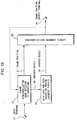
- a frame synchronization code detector shown in FIG. 18 may be used.
- the frame synchronization code detector shown in FIG. 18 is provided with a frame length detector 18 (refer to FIG. 4), detects the frame length information in the received data sequence from the received data input terminal 21 with this frame length detector 18, supplies the frame length information detected to a synchronization judgment circuit 23, and outputs it through a frame length information output terminal 9.
- the symbol 8 in FIG. 18 designates a frame number detector, which detects a frame number in the received data sequence from the received data input terminal 21 to output it through a frame number output terminal 10.
- the present embodiment detects the position and length (period) of the data loss/insertion by determining the frame position in the forward and backward direction on time axis and also by checking the reference unique word and the received data sequence.
- a check disagreement may occur as well, so that the present embodiment operate normally even when the data loss/insertion does not occur in multiples of the arrangement interval of the unique word.
- FIG. 19 is a block diagram showing the composition of the frame synchronization circuit according to another embodiment.
- the second frame synchronization code detector 33 and the difference circuit 44 are removed, a data loss and data insertion period judgment circuit 54 is provided in place of the data loss and data insertion period judgment circuit 34, and a synchronization judgment circuit 55 is provided in place of the synchronization judgment circuit 35.
- the data loss and data insertion period judgment circuit 54 accumulates evaluation values of the checked result 40 and judges whether a data loss or data insertion has occurred based on whether the accumulation result exceeds the predetermined threshold value.
- the evaluation value for "0" (agreement) of the checked result 40 can be set as “-1" and for "1" (disagreement) as "+2”, and the predetermined threshold value can be set as "5".
- the accumulation result does not become less than "0".
- the frame synchronization code detector 32 checks the reference unique word and received data sequence in the forward direction to output the checked result 40, as shown in FIG. 20E.
- the contents of FIGs. 20A to 20E are similar to those of FIGs. 7A to 7E.
- the evaluation values corresponding to the checked result 40 are accumulated in the data loss and data insertion period judgment circuit 54.
- the checked result 40 keeps “0" until the third bit S3 in FIGs. 20A to 20G, so that the evaluation value is "-1" and the accumulation result keeps “0". This is because the accumulation result never becomes less than "0" as described above.
- FIG. 21A shows a received data sequence without code error
- FIG. 21B shows a received data sequence in which a data loss has occurred in a frame
- FIG. 21E shows both checked results.
- the checked results from the first bit S1 to the fourth bit S4 are "0".
- the checked results after the fifth bit S5 become random values corresponding to the contents of the data sequence.
- FIG. 21F One example of this random checked results are shown in FIG. 21F. Also, the accumulation result of evaluation value to this checked result is shown in FIG. 21G.
- the checked result 40 never returns to continuous "0", so that the accumulation result exceeds a threshold value at a certain point, and the judgment result shown in FIG. 21H becomes “0".
- this judgment result is transmitted to the synchronization judgment circuit 55, there is detected "synchronous error" caused by data loss.
- the synchronization judgment circuit 55 stops the output of the frame position, and outputs an instruction to the frame synchronization code detector 32 to make detect the unique word once again.
- the judgment result becomes "1" as in the case when the data loss has occurred, so that the output of the frame position may be stopped to detect the unique word once again.
- the threshold value in the present embodiment is set to a value which can detect a slightly longer error than an assumed one generally occurred in a transmission channel.
- the judgment result turns to "1" even though a data loss or data insertion has not occurred.
- the occurrence of such phenomenon means that the state of transmission channel is substantially deteriorated, so that even though a frame synchronization is retained, to obtain a correct received data can not be expected. Therefore, it is considered that a practical problem may not occur according to the judgment result of "1" in such a state.
Landscapes
- Engineering & Computer Science (AREA)
- Computer Networks & Wireless Communication (AREA)
- Signal Processing (AREA)
- Synchronisation In Digital Transmission Systems (AREA)
- Time-Division Multiplex Systems (AREA)
Applications Claiming Priority (3)
| Application Number | Priority Date | Filing Date | Title |
|---|---|---|---|
| JP29411/97 | 1997-02-13 | ||
| JP2941197 | 1997-02-13 | ||
| PCT/JP1998/000557 WO1998036519A1 (fr) | 1997-02-13 | 1998-02-12 | Circuit de synchronisation de trames |
Publications (3)
| Publication Number | Publication Date |
|---|---|
| EP0905941A1 true EP0905941A1 (fr) | 1999-03-31 |
| EP0905941A4 EP0905941A4 (fr) | 2004-10-27 |
| EP0905941B1 EP0905941B1 (fr) | 2006-12-27 |
Family
ID=12275397
Family Applications (1)
| Application Number | Title | Priority Date | Filing Date |
|---|---|---|---|
| EP98902191A Expired - Lifetime EP0905941B1 (fr) | 1997-02-13 | 1998-02-12 | Circuit de synchronisation de trames |
Country Status (8)
| Country | Link |
|---|---|
| US (1) | US6738393B2 (fr) |
| EP (1) | EP0905941B1 (fr) |
| JP (1) | JP3511520B2 (fr) |
| KR (1) | KR100292249B1 (fr) |
| CN (2) | CN1282319C (fr) |
| CA (1) | CA2251822C (fr) |
| DE (1) | DE69836711T2 (fr) |
| WO (1) | WO1998036519A1 (fr) |
Cited By (3)
| Publication number | Priority date | Publication date | Assignee | Title |
|---|---|---|---|---|
| EP1178620A1 (fr) * | 2000-07-31 | 2002-02-06 | Koninklijke Philips Electronics N.V. | Procédé et systeme pour la synchronisation de trame |
| WO2002065677A1 (fr) * | 2001-02-13 | 2002-08-22 | Pervasic Limited | Protocole de paquets a synchronisation automatique pour communications radio |
| EP1126637A3 (fr) * | 2000-02-16 | 2003-09-03 | Lg Electronics Inc. | Méthode de synchronisation de trames par utilisation d'une séquence pilote dans un mode comprimé |
Families Citing this family (20)
| Publication number | Priority date | Publication date | Assignee | Title |
|---|---|---|---|---|
| US6930995B1 (en) * | 1999-06-23 | 2005-08-16 | Cingular Wireless Ii, Llc | Apparatus and method for synchronization in a multiple-carrier communication system by observing a plurality of synchronization indicators |
| JP2001156761A (ja) * | 1999-11-29 | 2001-06-08 | Ando Electric Co Ltd | パターン同期回路 |
| US6959014B2 (en) * | 2001-02-01 | 2005-10-25 | Freescale Semiconductor, Inc. | Method and apparatus for operating a communication bus |
| US6959015B1 (en) * | 2001-05-09 | 2005-10-25 | Crest Microsystems | Method and apparatus for aligning multiple data streams and matching transmission rates of multiple data channels |
| EP1753244B1 (fr) * | 2002-01-22 | 2010-04-14 | Microsoft Corporation | Procedes et systemes anti-emulation de code initial et de remplissage de donnees |
| GB0205142D0 (en) * | 2002-03-05 | 2002-04-17 | Nokia Corp | Synchronisation in communication systems |
| JP4155088B2 (ja) * | 2003-04-18 | 2008-09-24 | 日本電気株式会社 | 情報処理装置 |
| US7627004B2 (en) * | 2005-05-26 | 2009-12-01 | Cisco Technology, Inc. | Transporting synchronization channel information across a packet network |
| JP4910807B2 (ja) * | 2006-03-23 | 2012-04-04 | 富士通セミコンダクター株式会社 | 再生装置及び再生方法 |
| JP4565011B2 (ja) * | 2008-03-14 | 2010-10-20 | 株式会社日立製作所 | デジタル放送多重装置 |
| US9015562B1 (en) * | 2008-08-18 | 2015-04-21 | Marvell International Ltd. | Systems and methods for multistage error correction |
| CN102104414A (zh) * | 2009-12-17 | 2011-06-22 | 华为技术有限公司 | 一种定帧的方法和装置 |
| JP5419018B2 (ja) | 2010-06-14 | 2014-02-19 | 独立行政法人産業技術総合研究所 | スペクトル拡散通信システム |
| JP2014165723A (ja) * | 2013-02-26 | 2014-09-08 | Nec Engineering Ltd | フレーム同期装置、フレーム同期方法及びフレーム同期装置の制御プログラム |
| JP6056606B2 (ja) * | 2013-03-28 | 2017-01-11 | 富士通株式会社 | デスクランブル回路及びデスクランブル方法 |
| CN104579566B (zh) * | 2014-12-31 | 2018-02-09 | 中国电子科技集团公司第七研究所 | 同步信息检测方法、系统及通用相关器 |
| CN105162440B (zh) * | 2015-08-21 | 2018-01-02 | 四川九洲电器集团有限责任公司 | 一种同步检测装置 |
| US10271069B2 (en) | 2016-08-31 | 2019-04-23 | Microsoft Technology Licensing, Llc | Selective use of start code emulation prevention |
| DE102016118269A1 (de) * | 2016-09-27 | 2018-03-29 | Endress + Hauser Gmbh + Co. Kg | Verfahren und System zum verteilten Speichern von Informationen in einer eine Vielzahl von Feldgeräten aufweisenden Anlage der Prozessautomatisierung |
| US10313102B2 (en) * | 2016-12-22 | 2019-06-04 | Macom Connectivity Solutions, Llc | Power optimization mechanisms for framers by selectively deactivating frame alignment process |
Family Cites Families (20)
| Publication number | Priority date | Publication date | Assignee | Title |
|---|---|---|---|---|
| JPS6253040A (ja) * | 1985-09-02 | 1987-03-07 | Nippon Telegr & Teleph Corp <Ntt> | 復号回路 |
| JPS631128A (ja) * | 1986-06-20 | 1988-01-06 | Fujitsu Ltd | 同期化制御方式 |
| JPH01251930A (ja) | 1988-03-31 | 1989-10-06 | Toshiba Corp | フレーム同期検出方式 |
| FR2631762B1 (fr) * | 1988-05-18 | 1991-02-15 | Cit Alcatel | Dispositif de synchronisation de trame pour un train numerique synchrone partage en blocs au moyen d'un code par blocs et structure en trames |
| JPH02151144A (ja) * | 1988-12-02 | 1990-06-11 | Oki Electric Ind Co Ltd | フレーム同期回路 |
| JPH04328919A (ja) * | 1991-04-26 | 1992-11-17 | Fujitsu Ltd | 無線呼出し信号方式 |
| US5390199A (en) | 1991-07-19 | 1995-02-14 | Anritsu Corporation | Advanced code error detection apparatus and system using maximal-length pseudorandom binary sequence |
| JP2970717B2 (ja) | 1992-03-17 | 1999-11-02 | 三菱電機株式会社 | フレ−ム同期回路 |
| US5835023A (en) * | 1993-02-25 | 1998-11-10 | Ntt Mobile Communications Network Inc. | Selective radio paging system and pager |
| WO1995018494A1 (fr) * | 1993-12-29 | 1995-07-06 | Zenith Electronics Corporation | Structure de trames d'informations pour des constellations de donnees de taille variable |
| JPH07250055A (ja) * | 1994-03-09 | 1995-09-26 | Toshiba Corp | フレーム同期回路 |
| US5481572A (en) * | 1994-08-02 | 1996-01-02 | Ericsson Inc. | Method of and apparatus for reducing the complexitiy of a diversity combining and sequence estimation receiver |
| JPH0856356A (ja) * | 1994-08-10 | 1996-02-27 | Fujitsu Ltd | 符号化装置および復号化装置 |
| JPH08139714A (ja) | 1994-11-10 | 1996-05-31 | Hitachi Ltd | フレーム同期方式 |
| EP1802135A3 (fr) * | 1995-03-15 | 2008-11-12 | Kabushiki Kaisha Toshiba | Systèmes de codage et/ou de décodage d'images mobiles |
| US5790588A (en) * | 1995-06-07 | 1998-08-04 | Ntt Mobile Communications Network, Inc. | Spread spectrum transmitter and receiver employing composite spreading codes |
| JP3483991B2 (ja) * | 1995-07-27 | 2004-01-06 | 沖電気工業株式会社 | 符号分割多重アクセス通信用拡散符号発生器、符号分割多重アクセス通信システム及び符号分割多重アクセス通信用拡散符号発生方法 |
| US5757869A (en) * | 1995-07-28 | 1998-05-26 | Adtran, Inc. | Apparatus and method for detecting frame synchronization pattern/word in bit-stuffed digital data frame |
| CA2214743C (fr) * | 1996-09-20 | 2002-03-05 | Ntt Mobile Communications Network Inc. | Un circuit de synchronisation des trames et systeme de communication. |
| JPH11145945A (ja) * | 1997-11-12 | 1999-05-28 | Fujitsu Ltd | 符号化フレーム同期方法及び符号化フレーム同期回路 |
-
1998
- 1998-02-12 US US09/171,216 patent/US6738393B2/en not_active Expired - Fee Related
- 1998-02-12 CN CNB988001322A patent/CN1282319C/zh not_active Expired - Fee Related
- 1998-02-12 JP JP52240298A patent/JP3511520B2/ja not_active Expired - Fee Related
- 1998-02-12 WO PCT/JP1998/000557 patent/WO1998036519A1/fr not_active Ceased
- 1998-02-12 CA CA002251822A patent/CA2251822C/fr not_active Expired - Fee Related
- 1998-02-12 DE DE69836711T patent/DE69836711T2/de not_active Expired - Lifetime
- 1998-02-12 CN CN2006100958336A patent/CN1953359B/zh not_active Expired - Fee Related
- 1998-02-12 EP EP98902191A patent/EP0905941B1/fr not_active Expired - Lifetime
- 1998-02-12 KR KR1019980708319A patent/KR100292249B1/ko not_active Expired - Fee Related
Cited By (5)
| Publication number | Priority date | Publication date | Assignee | Title |
|---|---|---|---|---|
| EP1126637A3 (fr) * | 2000-02-16 | 2003-09-03 | Lg Electronics Inc. | Méthode de synchronisation de trames par utilisation d'une séquence pilote dans un mode comprimé |
| US6947476B2 (en) | 2000-02-16 | 2005-09-20 | Lg Electronics Inc. | Method for synchronizing frame by using pilot pattern in compressed mode |
| EP1178620A1 (fr) * | 2000-07-31 | 2002-02-06 | Koninklijke Philips Electronics N.V. | Procédé et systeme pour la synchronisation de trame |
| US7058879B2 (en) | 2000-07-31 | 2006-06-06 | Koninklijke Philips Electronics N.V. | Data transmission system, equipment suitable for such a system and data transmission method |
| WO2002065677A1 (fr) * | 2001-02-13 | 2002-08-22 | Pervasic Limited | Protocole de paquets a synchronisation automatique pour communications radio |
Also Published As
| Publication number | Publication date |
|---|---|
| CA2251822C (fr) | 2003-11-11 |
| CN1953359B (zh) | 2011-06-01 |
| KR20000064941A (ko) | 2000-11-06 |
| EP0905941A4 (fr) | 2004-10-27 |
| CN1217843A (zh) | 1999-05-26 |
| CA2251822A1 (fr) | 1998-08-20 |
| CN1282319C (zh) | 2006-10-25 |
| KR100292249B1 (ko) | 2001-06-01 |
| DE69836711D1 (de) | 2007-02-08 |
| CN1953359A (zh) | 2007-04-25 |
| DE69836711T2 (de) | 2007-10-04 |
| EP0905941B1 (fr) | 2006-12-27 |
| JP3511520B2 (ja) | 2004-03-29 |
| US20030189954A1 (en) | 2003-10-09 |
| WO1998036519A1 (fr) | 1998-08-20 |
| US6738393B2 (en) | 2004-05-18 |
Similar Documents
| Publication | Publication Date | Title |
|---|---|---|
| EP0905941B1 (fr) | Circuit de synchronisation de trames | |
| CA1195007A (fr) | Systeme d'encadrement | |
| JPWO1998036519A1 (ja) | フレーム同期回路 | |
| US20030037297A1 (en) | Frame synchronization device and frame synchronization method | |
| USRE40918E1 (en) | Method and device for transmitting data frames | |
| US6266349B1 (en) | Method and apparatus for detecting frame in data stream | |
| JP4629201B2 (ja) | 同期階層ネットワークシステム中でデータを伝送する方法および同期階層ネットワークシステム | |
| US6693919B1 (en) | Frame synchronization method and frame synchronization circuit | |
| JP2861932B2 (ja) | バーストフレーム位相同期回路 | |
| WO1986004203A1 (fr) | Systeme de traitement de donnees de transmission | |
| US20040117499A1 (en) | System and method for detection of delineation of data units for a communication element | |
| CA2296396C (fr) | Procede et dispositif permettant d'emettre des donnees dans un systeme de communication de donnees multiplexe a grande vitesse | |
| US4967411A (en) | Method and apparatus for frame-bit modulation and demodulation of DS3 signal | |
| US8218701B2 (en) | Communication system | |
| CA2201805C (fr) | Appareil de traitement de reception de message de synchronisation | |
| JP3234758B2 (ja) | バースト同期回路 | |
| JP2000174670A (ja) | 伝送路切替装置 | |
| JPS60213150A (ja) | 符号方式 | |
| US6516003B1 (en) | Data communication apparatus | |
| JP2001308814A (ja) | フレーム構成自動識別通信装置 | |
| JP2001197051A (ja) | 同期回路 | |
| JPH01311739A (ja) | 同期語検出確定方式 | |
| JPH037439A (ja) | ディジタル通信回線の監視方式 | |
| KR20030041281A (ko) | 순번을 가진 유토피아 프로토콜 구현 방법 | |
| KR20040010931A (ko) | 통신 시스템에서의 일반 프레이밍 절차 프레임 경계 검출회로 |
Legal Events
| Date | Code | Title | Description |
|---|---|---|---|
| PUAI | Public reference made under article 153(3) epc to a published international application that has entered the european phase |
Free format text: ORIGINAL CODE: 0009012 |
|
| 17P | Request for examination filed |
Effective date: 19980828 |
|
| AK | Designated contracting states |
Kind code of ref document: A1 Designated state(s): DE FR GB IT SE |
|
| A4 | Supplementary search report drawn up and despatched |
Effective date: 20040914 |
|
| 17Q | First examination report despatched |
Effective date: 20050111 |
|
| GRAP | Despatch of communication of intention to grant a patent |
Free format text: ORIGINAL CODE: EPIDOSNIGR1 |
|
| GRAS | Grant fee paid |
Free format text: ORIGINAL CODE: EPIDOSNIGR3 |
|
| GRAA | (expected) grant |
Free format text: ORIGINAL CODE: 0009210 |
|
| AK | Designated contracting states |
Kind code of ref document: B1 Designated state(s): DE FR GB IT SE |
|
| REG | Reference to a national code |
Ref country code: GB Ref legal event code: FG4D |
|
| REF | Corresponds to: |
Ref document number: 69836711 Country of ref document: DE Date of ref document: 20070208 Kind code of ref document: P |
|
| REG | Reference to a national code |
Ref country code: SE Ref legal event code: TRGR |
|
| ET | Fr: translation filed | ||
| PLBE | No opposition filed within time limit |
Free format text: ORIGINAL CODE: 0009261 |
|
| STAA | Information on the status of an ep patent application or granted ep patent |
Free format text: STATUS: NO OPPOSITION FILED WITHIN TIME LIMIT |
|
| 26N | No opposition filed |
Effective date: 20070928 |
|
| PGFP | Annual fee paid to national office [announced via postgrant information from national office to epo] |
Ref country code: FR Payment date: 20120221 Year of fee payment: 15 |
|
| PGFP | Annual fee paid to national office [announced via postgrant information from national office to epo] |
Ref country code: DE Payment date: 20120208 Year of fee payment: 15 |
|
| PGFP | Annual fee paid to national office [announced via postgrant information from national office to epo] |
Ref country code: IT Payment date: 20120223 Year of fee payment: 15 Ref country code: GB Payment date: 20120208 Year of fee payment: 15 Ref country code: SE Payment date: 20120215 Year of fee payment: 15 |
|
| REG | Reference to a national code |
Ref country code: SE Ref legal event code: EUG |
|
| GBPC | Gb: european patent ceased through non-payment of renewal fee |
Effective date: 20130212 |
|
| PG25 | Lapsed in a contracting state [announced via postgrant information from national office to epo] |
Ref country code: SE Free format text: LAPSE BECAUSE OF NON-PAYMENT OF DUE FEES Effective date: 20130213 |
|
| REG | Reference to a national code |
Ref country code: FR Ref legal event code: ST Effective date: 20131031 |
|
| REG | Reference to a national code |
Ref country code: DE Ref legal event code: R119 Ref document number: 69836711 Country of ref document: DE Effective date: 20130903 |
|
| PG25 | Lapsed in a contracting state [announced via postgrant information from national office to epo] |
Ref country code: IT Free format text: LAPSE BECAUSE OF NON-PAYMENT OF DUE FEES Effective date: 20130212 |
|
| PG25 | Lapsed in a contracting state [announced via postgrant information from national office to epo] |
Ref country code: GB Free format text: LAPSE BECAUSE OF NON-PAYMENT OF DUE FEES Effective date: 20130212 Ref country code: DE Free format text: LAPSE BECAUSE OF NON-PAYMENT OF DUE FEES Effective date: 20130903 Ref country code: FR Free format text: LAPSE BECAUSE OF NON-PAYMENT OF DUE FEES Effective date: 20130228 |