EP0908827B1 - Dispositif d'interface de mémoire et dispositif de génération d'adresses de mémoire - Google Patents
Dispositif d'interface de mémoire et dispositif de génération d'adresses de mémoire Download PDFInfo
- Publication number
- EP0908827B1 EP0908827B1 EP98118641A EP98118641A EP0908827B1 EP 0908827 B1 EP0908827 B1 EP 0908827B1 EP 98118641 A EP98118641 A EP 98118641A EP 98118641 A EP98118641 A EP 98118641A EP 0908827 B1 EP0908827 B1 EP 0908827B1
- Authority
- EP
- European Patent Office
- Prior art keywords
- output
- signal
- buffer
- input
- single port
- Prior art date
- Legal status (The legal status is an assumption and is not a legal conclusion. Google has not performed a legal analysis and makes no representation as to the accuracy of the status listed.)
- Expired - Lifetime
Links
Images






Classifications
-
- G—PHYSICS
- G06—COMPUTING OR CALCULATING; COUNTING
- G06F—ELECTRIC DIGITAL DATA PROCESSING
- G06F9/00—Arrangements for program control, e.g. control units
- G06F9/06—Arrangements for program control, e.g. control units using stored programs, i.e. using an internal store of processing equipment to receive or retain programs
- G06F9/30—Arrangements for executing machine instructions, e.g. instruction decode
- G06F9/34—Addressing or accessing the instruction operand or the result ; Formation of operand address; Addressing modes
- G06F9/345—Addressing or accessing the instruction operand or the result ; Formation of operand address; Addressing modes of multiple operands or results
-
- G—PHYSICS
- G06—COMPUTING OR CALCULATING; COUNTING
- G06F—ELECTRIC DIGITAL DATA PROCESSING
- G06F13/00—Interconnection of, or transfer of information or other signals between, memories, input/output devices or central processing units
- G06F13/14—Handling requests for interconnection or transfer
- G06F13/16—Handling requests for interconnection or transfer for access to memory bus
- G06F13/1668—Details of memory controller
- G06F13/1673—Details of memory controller using buffers
-
- H—ELECTRICITY
- H04—ELECTRIC COMMUNICATION TECHNIQUE
- H04N—PICTORIAL COMMUNICATION, e.g. TELEVISION
- H04N19/00—Methods or arrangements for coding, decoding, compressing or decompressing digital video signals
- H04N19/42—Methods or arrangements for coding, decoding, compressing or decompressing digital video signals characterised by implementation details or hardware specially adapted for video compression or decompression, e.g. dedicated software implementation
- H04N19/423—Methods or arrangements for coding, decoding, compressing or decompressing digital video signals characterised by implementation details or hardware specially adapted for video compression or decompression, e.g. dedicated software implementation characterised by memory arrangements
-
- H—ELECTRICITY
- H04—ELECTRIC COMMUNICATION TECHNIQUE
- H04N—PICTORIAL COMMUNICATION, e.g. TELEVISION
- H04N19/00—Methods or arrangements for coding, decoding, compressing or decompressing digital video signals
- H04N19/60—Methods or arrangements for coding, decoding, compressing or decompressing digital video signals using transform coding
- H04N19/61—Methods or arrangements for coding, decoding, compressing or decompressing digital video signals using transform coding in combination with predictive coding
Definitions
- the present invention relates to a digital signal processing system including a memory interface device for writing and reading a digital signal to/from a single port memory.
- Video signal formats including NTSC, PAL, HDTV, VGA and SVGA
- display devices including a CRT, an LCD (liquid crystal display) and a plasma display. It is required to process digital video signals of the various formats in a single display (television) system.
- a digital signal processing system using a memory is essential for converting one video signal format tc another, and/or for synthesizing two or more non-synchronous video signals together.
- a highspeed, real-time data processing method is required for writing and reading the video signals without a break.
- a dual port memory such as a FIFO is used for writing and reading the video signals to/from a memory in real time.
- two single port memories are used, and the real time processing is achieved by alternately controlling the write and read operations to/from the two single port memories.
- special purpose memory control devices are provided for converting the video signal format and for processing a plurality of non-synchronous video signals, respectively.
- processing video signals in real time requires at least two single port memories or a single dual port memory, thereby making the entire system expensive.
- usable bit width and clock frequency of the video signal are limited even when such a memory arrangement is provided, a flexible system may not be realized.
- Processing video signals of different formats requires a digital signal processing system capable of processing each video signal in real time using a memory at a rate associated with the signal format. Accordingly, address control methods are also becoming more complicated.
- a conventional memory control device uses special purpose hardware for calculating the memory address for each of a plurality of address pointers.
- a conventional display (television) system which processes different video signal formats needs a number of special purpose hardwares for controlling the memory addresses in different manners in accordance with the different video signal formats, thereby tending to have a large scale circuit.
- an additional special purpose memory is needed for a frame synchronization process for converting a video signal in a synchronous system to another video signal in a different synchronous system.
- GB 2,311,153 A discloses the multiplexing access to a single port of a memory, wherein several devices are attached to the same port of a RAM each through a buffer. Control and address signals for the access required by each device are input to a multiplexer. A timing circuit causes the multiplexer to step cyclically through the control and address signals, presenting to the RAM the control and address signals from each device in turn. The corresponding buffer is also actuated by the timing circuit for data input/output with the RAM. Separate external data ports to which devices which will share access to the RAM are connected to bidirectional input ports of the respective buffers. Outputs of each of the buffers are connected to a data bus of the RAM, whereby data can be transferred to and from the data port of the RAM.
- Each buffer can comprise a bus transceiver with latches in both transmission directions. Write data is stored in the buffer until the timeslot corresponding to port allows data be written in the RAM. During a read operation, data is latched from the data port of the RAM into the addressed buffer during its timeslot.
- the timing circuit is connected to the control port of the multiplexer, and to address inputs of the buffers. The timing circuit can cyclically count sequentially and outputs cyclically repeating binary count signals. These signals are used as a control signal to multiplexer whereby the address and control signals appearing at respective inputs to the multiplexer are sequentially applied to its output, and therefore to the address and control port of the RAM.
- the invention described herein makes possible at least one of the advantages of: (1) providing a memory interface device capable of processing a video signal in real time using one single port memory; (2) providing a memory interface device capable of processing a video signal in real time using one single port memory, and realizing a system which is independent of a bit number of an input/output signal or a bus width of the single port memory; (3) providing a memory interface device capable of processing a video signal in real time using one single port memory, which enables signal processing of a plurality of non-synchronous video signals.
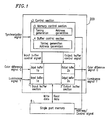
- Figure 1 illustrates a memory interface device 200 according to Example 1 of the present invention.
- the memory interface device 200 includes an input buffer section 1, an output buffer section 2 and a control section 3.
- the control section 3 controls the input buffer section 1, the output buffer section 2 and a single port memory 6.
- the control section 3 outputs an input buffer control signal to the input buffer section 1 and an output buffer control signal to the output buffer section 2 in response to a synchronization signal.
- the control section 3 receives request signals from the input buffer section 1 and the output buffer section 2 for accessing the single port memory 6, and outputs an address, a control signal, or the like, to the single port memory 6 in response to the access request signal.
- the signal input to the memory interface device 200 is a video signal which includes a luminance signal Y and a color difference signal C .
- the input buffer section 1 includes an input buffer 1a for receiving the luminance signal Y and another input buffer 1b for receiving the color difference signal C.
- the output buffer section 2 includes an output buffer 2a for outputting the luminance signal Y and another output buffer 2b for outputting the color difference signal C.
- the luminance signal Y is stored in the single port memory 6 via the input buffer 1a, and the luminance signal Y read out from the single port memory 6 is output via the output buffer 2a.
- the color difference signal C is stored in the single port memory 6 via the input buffer 1b, and the color difference signal C read out from the single port memory 6 is output via the output buffer 2b.
- the input buffer section 1 and the output buffer section 2 are preferably divided into two subsections for different signals in the present example, such division is not necessary for the present invention.
- the input buffer section 1 may include only one input buffer
- the output buffer section 2 may include only one output buffer. Such an embodiment is within the scope of the present invention.
- Figure 2 illustrates the input buffer 1a.
- the input buffer 1b preferably has the same structure as that of the input buffer 1a.
- a black dot 7 and a white dot 8 each represent a memory cell for storing one bit of data.
- the black dot 7 represents a memory cell storing one bit of data
- the white dot 8 represents an empty memory cell storing no data.
- the bit width of the signal (the luminance signal Y) input to the input buffer 1a is n bits
- the total size of the input buffer 1a is m ⁇ n bits, where n is a positive integer and m is n ⁇ 2.
- the input signal is stored in one or more columns of memory cells, starting from the 0 th column.
- the input signal is stored in the 0 th to 2 nd columns of memory cells.
- the input buffer 1a is logically divided into two areas I 1 and I 2 .
- the area I 1 includes the O th to (m-2)/2 th columns of memory cells, and the area I 2 includes the m/2 th to (m-1) th columns of memory cells.
- a write operation (transfer) of data from the input buffer 1a to the single port memory 6 occurs when one of the areas I 1 and I 2 is filled with data.
- Figure 3 shows timing diagrams illustrating an operation for writing the input signal to the single port memory 6 after the input signal is temporarily stored in the input buffer 1a.
- the timing of writing the input signal to the single port memory 6 after the input signal is temporarily stored in the input buffer 1b is substantially the same as that illustrated in Figure 3.
- a horizontal synchronization signal is used as a reference signal, though any other signal may alternatively be used as the reference signal.
- An input buffer enable signal indicates whether or not to enable a write operation to the input buffer 1a.
- a high level input buffer enable signal indicates an enabling state
- a low level input buffer enable signal indicates a disabling state.
- the control section 3 outputs the input buffer enable signal to the input buffer 1a.
- the input buffer enable signal is a type of input buffer control signal.
- a request for writing data to the single port memory 6 is generated when one of the areas I 1 and I 2 is filled with data. Therefore, while the input buffer enable signal is at the high level, the request for writing data to the single port memory 6 is generated for each cycle of m/2.
- the input buffer 1a may generally be divided into L areas (L is a natural number greater than or equal to 2).
- the input signal may have any number of bits, as long as the number of bits is equal to or less than the row address size of the input buffer 1a. The same applies to the input buffer 1b.
- FIG. 4 illustrates the output buffer 2a.
- the output buffer 2b has the same structure as that of the output buffer 2a.
- a black dot 7 and a white dot 8 each represent a memory cell for storing one bit of data.
- the black dot 7 represents a memory cell storing one bit of data
- the white dot 8 represents an empty memory cell storing no data.
- the bit width of the signal (the luminance signal Y) output from the output buffer 2a is n bits
- the total size of the output buffer 2a is m ⁇ n bits, where n and m are each a positive integer.
- the output signal is output from one or more columns of memory cells, starting from the 0 th column.
- the data has been output from the 0 th to 2 nd columns of memory cells.
- the output buffer 2a is logically divided into two areas O 1 and O 2 .
- the area O 1 includes the O th to (m-2)/2 th columns of memory cells, and the area O 2 includes the m/2 th to (m-1) th columns of memory cells.
- a read operation (transfer) of data from the single port memory 6 to the output buffer 2a occurs when one of the areas O 1 and O 2 becomes empty.
- Figure 5 shows timing diagrams illustrating an operation for externally outputting data from the memory interface device 200 after the data is read out from the single port memory 6 and temporarily stored in the output buffer 2a.
- the timing of externally outputting data from the memory interface device 200 after the data is read out from the single port memory 6 and temporarily stored in the output buffer 2b is substantially the same as that illustrated in Figure 5.
- a horizontal synchronization signal is used as a reference signal, though any other signal may alternatively be used as the reference signal.
- An output buffer enable signal indicates whether or not to enable a read operation from the output buffer 2a.
- a high level output buffer enable signal indicates an enabling state
- a low level output buffer enable signal indicates a disabling state.
- the control section 3 outputs the output buffer enable signal to the output buffer 2a.
- the output buffer enable signal is a type of output buffer control signal.
- a request for reading out data from the single port memory 6 is generated when one of the areas O 1 and O 2 becomes empty. Therefore, while the output buffer enable signal is at the high level, the request for reading out data from the single port memory 6 is generated for each cycle of m/2 (a period for accessing m/2 columns of memory cells).
- the data stored in the area O 1 of the output buffer 2a starts to be output. While the data stored in the area O 1 of the output buffer 2a is being output, another output signal is read out from the single port memory 6, and transferred to and written in the area O 2 of the output buffer 2a. Subsequently, the same process is repeated.
- the output buffer 2a may generally be divided into N areas (N is a natural number greater than or equal to 2).
- the output signal may have any number of bits, as long as the number of bits is equal to or less than the row address size of the output buffer 2a. The same applies to the output buffer 2b.
- control section 3 When the control section 3 receives a write request from the input buffers 1a and 1b, the control section 3 controls the input buffers 1a and 1b so as to transfer data from the input buffers 1a and 1b to the single port memory 6, and outputs an address and a control signal to the single port memory 6. The transferred data is stored in the address in the single port memory 6.
- control section 3 When the control section 3 receives a read request from the output buffers 2a and 2b, the control section 3 outputs an address and a control signal to the single port memory 6.
- the single port memory 6 reads out data from the address in the single port memory 6, and transfers the data to the output buffers 2a and 2b.
- the control section 3 controls the output buffers 2a and 2b so as to store the data in the output buffers 2a and 2b.
- Figure 6 shows timing diagrams illustrating an operation for performing a write operation (for writing a video signal to the single port memory 6 while storing the video signal in the input buffers 1a and 1b) and a read operation (for reading out a video signal from the single port memory 6 while storing the video signal in the output buffers 2a and 2b) in parallel using the memory interface device 200 having the structure illustrated in Figure 1.
- a horizontal synchronization signal is used as a reference signal, though any other signal may alternatively be used as the reference signal.
- a first set of requests for reading out data from the single port memory 6 (including a request for reading out the luminance signal Y and a request for reading out the color difference signal C) are sent to the control section 3.
- the control section 3 reads out the luminance signal Y and the color difference signal C from the single port memory 6 in this order, and transfers the luminance signal Y to the area O 1 of the output buffer 2a and the color difference signal C to the area O 1 of the output buffer 2b.
- the input buffer enable signal and the output buffer enable signal go high at the same time.
- the next set of requests for reading out data from the single port memory 6 (including a request for reading out the luminance signal Y and a request for reading out the color difference signal C) are sent to the control section 3.
- the control section 3 reads out the luminance signal Y and the color difference signal C from the single port memory 6 in this order, and transfers the luminance signal Y to the area O 2 of the output buffer 2a and the color difference signal C to the area O 2 of the output buffer 2b.
- the control section 3 transfers and writes the luminance signal Y (stored in the area I 1 of the input buffer 1a ) and the color difference signal C (stored in the area I 1 of the input buffer 1b ) to the single port memory 6 in this order. Then, the luminance signal Y and the color difference signal C are read out in this order from the single port memory 6. The luminance signal Y is transferred to and written in the area O 1 of the output buffer 2a, and the color difference signal C to the area O 1 of the output buffer 2b.
- the write and read operations of data to/from the single port memory 6 are each performed within one cycle (m/2).
- the signals stored in the respective areas I 1 of the input buffers 1a and 1b are transferred to the single port memory 6, while the next input signals are stored in the respective areas I 2 of the input buffers 1a and 1b.
- the signals stored in the respective areas O 2 of the output buffers 2a and 2b are externally output, while the next signals are transferred from the single port memory 6 to the respective areas O 1 of the output buffers 2a and 2b. Subsequently, the same process is repeated.
- Figure 7 illustrates an exemplary memory map of the single port memory 6.
- a luminance signal Y1 and a color difference signal C1 for the first field are stored in addresses from 0 to n1-1 and in addresses from n1 to n2-1, respectively, of the single port memory 6.
- Luminance signals Y2 to Y4 and color difference signals C2 to C4 for the second to fourth fields are stored similarly in addresses from n2 to n8-1.
- the luminance signal Y2 and the color difference signal C2 for the second field are being input to the input buffer 1a and 1b, respectively, the luminance signal Y1 and the color difference signal C1 for the first field are being read out to the output buffers 2a and 2b, respectively.
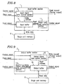
- Figure 8 illustrates the input buffer section 1.
- the input buffer section 1 is assumed to have only one input buffer 1c.
- the following description also applies to the case where the input buffer section 1 includes the two input buffers 1a and 1b, as in the example illustrated in Figure 1. It is also assumed that each input signal has 2 or 4 bits and that each word within the single port memory 6 also has 2 or 4 bits.
- the input buffer section 1 includes an input signal write control section 9, the input buffer 1c and an input data read control section 11.
- the input signal write control section 9 controls writing of an input signal.
- the input buffer 1c temporarily stores the input signal.
- the input data read control section 11 reads out the data stored in the input buffer 1c to the single port memory 6.
- FIG 9 illustrates the output buffer section 2.
- the output buffer section 2 is assumed to have only one output buffer 2c.
- the following description also applies to the case where the output buffer section 2 includes the two input buffers 2a and 2b, as in the example illustrated in Figure 1.
- the output buffer section 2 includes an output signal read control section 12, the output buffer 2c and an output data write control section 13.
- the output signal read control section 12 controls reading out of an output signal.
- the output buffer 2c temporarily stores the output signal.
- the output data write control section 13 stores the data read out from the single port memory 6 in the output buffer 2c.
- Video signals input to the input buffer section 1 are successively written in the input buffer 1c.
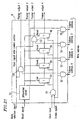
- FIG. 10 illustrates the input buffer 1c.
- the input buffer 1c includes a memory cell array 10 including memory cells 47 (each storing one bit of data).
- Reference numerals 20 to 27 each denote a pair of memory cells (each storing one bit of data).
- Reference numerals 28 to 37 each denote a wired OR.
- the input buffer 1c further includes flip flops 38 to 41, a multiplexer 42 for multiplexing data, selectors 43 and 44, and tristate buffers 45 and 46.
- the tristate buffers 45 and 46 each output the input signal intact when a control signal is at a low level. When the control signal is at a high level, the output impedance of the tristate buffers 45 and 46 becomes high and the tristate buffers 45 and 46 output no signal.
- the data bit width of the single port memory 6 is four, and one address is provided for every four bits accordingly.
- the memory cell array 10 is divided into two areas I 1 (for column addresses 0 and 1) and I 2 (for column addresses 2 and 3).
- the memory cell array 10 is also divided along the row direction into two sections having row addresses 0 and 1, respectively.
- the bits of the memory cells at each address are ORed with the corresponding bits of the memory bus.
- the input video signal has 4 bits, the signal is written in both of the row addresses 0 and 1.
- the input video signal has 2 bits, the signal is written only in the row address 0.
- the first data (2 bits) is stored in the memory cell pair 20 at the address (0 (row), 0 (column)) during one cycle, and the second data (2 bits) is stored in the memory cell pair 22 at (0, 1) during the following cycle.
- data is stored in all the memory cell pairs in the row address 1 in the area I 1 , and the data is read out to the memory bus to start writing the data to the single port memory 6.
- the data stored in the memory cell pair 20 and the data stored in the memory cell 22 are read out through the wired OR 28 and the wired OR 32, respectively, so as to form and output 4-bit data to the flip flops 38 to 41.
- a clock signal having the same frequency as the frequency with which data is written in the single port memory 6 is input to the flip flops 38 to 41.
- the select signal is switched to a low level
- the selector 43 outputs the signal from the flip flop 38 to the single port memory 6 and the selector 44 outputs the signal from the flip flop 39 to the single port memory 6.
- the tristate buffer 45 outputs the signal from the flip flop 40 to the single port memory 6, and the tristate buffer 46 outputs the signal from the flip flop 41 to the single port memory 6.
- the data output from the input buffer 1c has 4 bits, and thus the input buffer 1c can be connected to a single port memory having a bit width of 4 bits.
- a clock signal having a frequency which is one half of the frequency with which data is written in the single port memory 6 is input to the flip flops 38 to 41.
- the multiplexer 42 receives inputs from the flip flops 38 to 41.
- One of the flip flops 38 and 40 is selected to be the first output of the multiplexer 42.
- the data from the flip flop 38 is output when the clock signal is at the high level, and the data from the flip flop 40 is output when the clock signal is at the low level.
- one of the flip flops 39 and 41 is selected to be the second output of the multiplexer 42.
- the data from the flip flop 39 is output when the clock signal is at the high level, and the data from the flip flop 41 is output when the clock signal is at the low level. Therefore, the multiplexer 42 outputs data at a data rate twice as high as the clock signal.
- the selector 43 In response to the selection signal being at the high level, the selector 43 outputs the first output of the multiplexer 42 to the single port memory 6, and the selector 44 outputs the second output of the multiplexer 42 to the single port memory 6.
- the output impedance of the tristate buffers 45 and 46 becomes high. Therefore, the data output from the input buffer 1c has 2 bits, and the input buffer 1c can be connected to a single port memory having a bit width of 2 bits.
- the data output to the single port memory 6 is performed in substantially the same manner also when data is stored in both of the memory cell pairs (24 and 26) in the area I 2 .
- the input signal is a data string of 4 bits
- the first data (4 bits) is stored in the memory cell pairs 20 and 21, and the second data (4 bits) is stored in the memory cell pairs 22 and 23.
- data is stored in all the memory cell pairs in the area I 1 , and the data is read out to the memory bus to start writing the data to the single port memory 6.
- the data stored in the memory cell pair 20 and the data stored in the memory cell pair 21 are first read out through the wired OR 28 and the wired OR 29, respectively, so as to form 4-bit data. Subsequently, the data stored in the memory cell pair 22 and the data stored in the memory cell pair 23 are read out through the wired OR 30 and the wired OR 31, respectively, so as to form and output 4-bit data to the flip flops 38 to 41.
- a 2-bit input data or a 4-bit data can be written in the single port memory 6 which has either 2 bits/word or 4 bits/word.
- This can also apply to the case where the input data is n-bit data (n is a natural number) and the single port memory 6 has m bits/word (m is a natural number).
- the structure of the memory cell array 10 can also be used for the output buffer section 2.
- the order in which the data is transferred to/from the plurality of areas is not limited to that of the present example, and any other order can be employed as long as all the buffered data can be transferred.
- Figure 11 illustrates the write control sec tion 9.
- the write control section 9 includes a differential circuit 50, AND gates 51 to 55 and flip flops 57 to 60.
- the differential circuit 50 receives a reset signal and outputs a signal having a width substantially equal to one clock. While the output of the differential circuit 50 is at the high level, the flip flop 57 is set to the high level, and the other flip flops 58 to 60 are each reset to the low level. This is the initial state of the write control section 9.
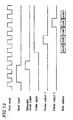
- Figure 12 shows timing diagrams illustrating an operation of the write control section 9.
- the output signals of the flip flops 58 and 60 are represented by pointer outputs 1 and 2.
- the output of the pointer 1 going high indicates that the area I 1 of the input buffer 1c is filled with data
- the output of the pointer 2 going high indicates that the area I 2 of the input buffer 1c is filled with data.
- the pointer output is output to the control section 3 as a request for writing data from the input buffer 1c to the single port memory 6.
- the pointer outputs 1 and 2 are each used to indicate that the output buffer 2c has become empty, so that a request is output to the control section 3 for reading out data from the single port memory 6.
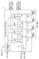
- Figure 13 illustrates the input data read control section 11.
- the read control section 11 includes AND gates 70 to 73.
- Each of the AND gates 70 to 73 decodes a control signal (address) output from the control section 3 so as to output a signal which indicates the column address of the corresponding area in the memory cell array 10.
- the structure of the output data write control section 13 may be substantially the same as that described above.
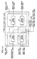
- Figure 14 illustrates the control section 3.
- the control section 3 includes a buffer control section 4 (including a timing generator 80 and an address generator 81) and a memory control section 5 (including another timing generator 82 and another address generator 83).
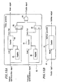
- Figure 15A illustrates the timing generator 80.
- the timing generator 80 includes counters 84 and 87, registers 85 and 88, RS flip flops 86 and 89 and an AND gate 90.
- a value of the register 85 is loaded to the counter 84.
- the counte r 84 starts counting from the next cycle, and outputs a carry out signal when the counter 84 has counted up to n.
- the carry out signal is a reset signal to the differential circuit 50 of the write control section 9 ( Figure 11) and a "set" signal to the RS flip flop 86.
- a value of the register 88 is loaded to the counter 87, and the RS flip flop 89 is reset.
- the counter 87 starts counting from the next cycle, and outputs a carry out signal when the counter 87 has counted up to m.
- the carry out signal is a "set" signal to the RS flip flop 89.
- An enable signal output from the AND gate 90 is at a high level while the outputs from the RS flip flops 86 and 89 are at a high level.
- Figure 15B illustrates the address generator 81.
- the address generator 81 includes a counter 91.
- the counter 91 In response to a pointer signal output from the input signal write control section 9, the counter 91 is reset. The counter 91 starts counting from the next cycle, and the count of the counter 91 is output to the input data read control section 11 as an address.
- the structure of the timing generator 82 and the structure of the address generator 83 may be substantially the same as the structure of the timing generator 80 and the structure of the address generator 81, respectively.
- the write control section 9 provides the two pointer outputs 1 and 2 since a buffer is divided into two areas. When a buffer is divided into more areas, more pointer outputs are provided accordingly. When a buffer is divided into L areas (L is a natural number greater than or equal to 2), L pointers are provided accordingly.
- the areas I 1 and I 2 can be further divided into four areas I 1 , I 2 , I 3 and I 4 having column addresses 0 to 4, respectively. In such a case, the outputs of the flip flops 57 to 60 are pointers 1 to 4, respectively.
- Figure 21 illustrates a write control section 9' according to a variation of the present example.
- the write control section 9' is similar to the write control section 9 but has four pointers 1 to 4.
- the write control section 9' includes the differential circuit 50, the AND gates 51 to 55, additional AND gates 130 and 131 and the flip flops 57 to 60.
- a mode selection signal is provided to the write control section 9' which is at a low level when the buffer is divided into two areas and at a high level when the buffer is divided into four areas.
- the output of the AND gate 130 is the pointer 1
- the output of the flip flop 58 is the pointer 2
- the output of the AND gate 131 is the pointer 3
- the output of the flip flop 60 is the pointer 4.
- the mode selection signal and the additional AND gates 130 and 131 are provided. Therefore, when the buffer is divided into two areas I 1 and I 2 , the mode selection signal is at the low level. Then, the pointer outputs 1 and 3 are always at the low level, thereby not starting a write operation to a memory. The write operation to the memory is initiated when the pointer output 2 or 4 goes high. When the buffer is divided into two areas I 1 and I 2 , the mode selection signal is at the high level. Then, any of the pointer outputs 1 to 4 going high initiates a write operation to the memory. In this way, it is possible to provide a section for selectively controlling a write operation to the single port memory 6 based on the size of the buffer area.
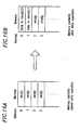
- Figures 16A and 16B each illustrate a memory map of the single port memory 6 when employing the write control section 9 illustrated in Figure 11.
- Figure 16A illustrates the initial state.
- Figure 16B illustrates the single port memory 6 when data has been written in the area I 1 .
- the minimum accessing unit of the single port memory 6 depends upon the size of the buffer area.
- Figures 17A to 17D each illustrate a memory map of the single port memory 6 when the buffer is further divided into four areas I 1 to I 4 .
- Figure 17A illustrates the initial state.
- Figure 17B illustrates the single port memory 6 when data has been written in the area I 1 .
- Figures 17C and 17D each illustrate the single port memory 6 when data has been written in the area I 2 .
- the minimum unit by which the memory address can be controlled depends upon the size of each buffer area. Therefore, by providing a section for selectively controlling the size of the buffer area, "fine" or high resolution memory address control can be performed.
- Figure 18 illustrates an arbitration circuit for arbitrating requests for writing data to the single port memory 6 and requests for reading data from the single port memory 6.
- the arbitration circuit may be included in the control section 3.
- the arbitration circuit includes registers 94 to 97 for user settings, AND gates 98 to 101 and an arbitrator 102.
- pointer outputs A to D are provided.
- the pointer output A indicates whether an input signal 1 is stored in the input buffer 1c, thereby filling up the input buffer 1c.
- the pointer output B indicates whether an input signal 2 is stored in the input buffer 1c, thereby filling up the input buffer 1c.
- the pointer output C indicates whether an output signal 1 is output from the output buffer 2c, thereby emptying the output buffer 2c.
- the pointer output D indicates whether an output signal 1 is output from the output buffer 2c, thereby emptying the output buffer 2c.
- the requests for writing and reading data to/from the single port memory 6 are prioritized, and the priority of each request is represented by the 2-bit value set in the register.
- the 2-bit value "11" indicates the first (highest) priority
- “10” indicates the second priority
- "01” indicates the third (lowest) priority
- "00" indicates "no request”.
- the priority may be represented by any suitable number of bits depending upon the particular application in which the memory interface device is used.
- the pointer output A goes high, and the value set in the register 94 is input via the AND gate 98 to the arbitrator 102 as a write request signal Write REQA.
- the value set in the register 95 is input to the arbitrator 102 as a write request signal Write REQB.
- the output signal 1 empties the first area I 1 of the output buffer 2c
- the value set in the register 96 is input to the arbitrator 102 as a read request signal Read REQA.
- the value set in the register 97 is input to the arbitrator 102 as a read request signal Read REQB.
- the arbitrator 102 has a preset priority sequence inherent within the particular arbitrator 102 hardware. Therefore, when more than one write requests or read request is issued, the requests are processed in accordance with the priority sequence.
- the signal write REQA has the first (highest) priority
- the signal Write REQB has the second priority
- the signal Read REQA has the third priority
- the signal Read REQB has the fourth (lowest) priority.
- Any other priority sequence can be applied by the user of the memory interface device by setting appropriate values in the registers 94 to 97. For example, "11" can be set in the register 97 to give the signal Read REQB the highest priority.
- Figure 19 is a chart illustrating various values output from the arbitrator 102 for various register settings.
- the first row (Row No. 1) represents a case where "11" is set in the register 94, and the pointer output A is accordingly at the high level.
- a signal Write Mode A of the single port memory 6 is always at the high level regardless of the other write and read requests being issued or the register settings.
- the arbitrator 102 processes the request from the pointer output A by the highest priority.
- the read control section 11 of the input buffer 1c processes the request for reading out data from the single port memory 6 by reading out data from the addresses (0, 0) and (0, 1). Then, the pointer output A returns to the low level.
- the second row (Row No. 2) of Figure 19 represents a case where "10" or a lower priority value is set in the register 94 while "11" is set in the register 95.
- a signal Write Mode B of the single port memory 6 is always at the high level regardless of the other write and read requests being issued or the register settings.
- the arbitrator 102 processes the request from the pointer output B as having the highest priority.
- the priority of the pointer output A is set to be "second” by setting "10” in the register 94, while the priority of the pointer output B is set to be “first” by setting "11” in the register 95.
- the other rows (Row Nos. 3 to 12) of Figure 19 show the same processing principle for different settings.
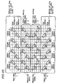
- Figure 20 illustrates a memory cell array 121 of the input buffer section 1, a write bus to the single port memory 6, a memory cell array 122 of the output buffer section 2, and a read bus from the single port memory 6.
- reference numerals 20 to 27 and 104 to 111 each denote a pair of memory cells.
- Reference numerals 28 to 36 and 112 to 120 each denote a pair of wired ORs. It is assumed in the present example that each word of the single port memory 6 has 4 bits.
- the data is normally output through the wired ORs 28 to 36 to the single port memory 6. Since a write bit line of the write memory bus and a read bit line of the read memory bus are connected together, it is possible to write data in the memory cell array 121. of the input buffer section 1 directly to the memory cell array 122 of the output buffer section 2. For example, when reading out data in the memory cell pair 20 through the wired OR 28, if the wired OR 112 is turned on, the data can be written in the memory cell pair 104.
- an input signal can be output with a delay using the input buffer 1c and the output buffer 2c.
- an input signal is delayed by 4 to 8 clocks.
- the number of bits or the number of words of the buffer of the present invention is not limited to those described above.
Landscapes
- Engineering & Computer Science (AREA)
- Theoretical Computer Science (AREA)
- Multimedia (AREA)
- Signal Processing (AREA)
- Software Systems (AREA)
- Physics & Mathematics (AREA)
- General Engineering & Computer Science (AREA)
- General Physics & Mathematics (AREA)
- Controls And Circuits For Display Device (AREA)
- Image Input (AREA)
- Dram (AREA)
- Information Transfer Systems (AREA)
Claims (5)
- Système de traitement de signaux numériques pour convertir un format de signal en temps réel en un autre et/ou pour synthétiser deux ou plus signaux en temps réel non synchrones ensembles, ledit système incluant une mémoire à un seul port, et
un dispositif d'interface mémoire (200), comprenant:une mémoire tampon d'entrée (1) incluant une pluralité de zones d'entrée ;une mémoire tampon de sortie (2) incluant une pluralité de zones de sortie; etune section de commande (3) pour commander la mémoire tampon d'entrée, la mémoire tampon de sortie et une mémoire à un seul port (6),dans lequel
la section de commande commande la mémoire tampon d'entrée (1) et la mémoire à un seul port (6) afin de transférer un signal stocké dans une des zones d'entrée de la mémoire tampon d'entrée vers la mémoire tampon à un seul port (6) tout en stockant un signal d'entrée dans une autre des zones d'entrée de la mémoire tampon d'entrée (1); et
la section de commande commande la mémoire tampon de sortie (2) et la mémoire à un seul port (6) afin de délivrer en sortie en tant que signal de sortie un signal stocké dans une des zones de sortie de la mémoire tampon de sortie (2) tout en transférant un signal stocké dans la mémoire à un seul port (6) vers une autre des zones de sortie de la mémoire tampon de sortie (2). - Système de traitement de signaux numériques selon la revendication 1, comprenant en outre un circuit de conversion de largeur de bus pour convertir une largeur de bus de sortie de la mémoire tampon d'entrée (1) en une largeur de bus d'entrée de la mémoire à un seul port (6), et convertir une largeur de bus de sortie de la mémoire à un seul port (6) en une largeur de bus d'entrée de la mémoire tampon de sortie (2).
- Système de traitement de signaux numériques selon la revendication 1, dans lequel la mémoire tampon d'entrée (1) est divisée le long d'une direction de ligne de bits et le long d'une direction d'une ligne de mots de la mémoire tampon d'entrée (1) en une pluralité de zones d'entrée, et la mémoire tampon de sortie (2) est divisée le long d'une direction de ligne de bits et le long d'une direction d'une ligne de mots de la mémoire tampon de sortie (2) en une pluralité de zones de sortie.
- Système de traitement de signaux numériques selon la revendication 1, dans lequel:chacune de la mémoire tampon d'entrée (1) et de la mémoire tampon de sortie (2) délivre en sortie vers la section de commande un signal de requête pour accéder à la mémoire à un seul port (6); etla section de commande (3) a un circuit d'arbitrage (102) pour donner une priorité d'accès aux signaux de requête en se basant sur une séquence de priorité prédéterminée.
- Système de traitement de signaux numériques selon la revendication 1, comprenant en outre un circuit pour écrire un signal provenant de la mémoire tampon d'entrée (1) directement dans la mémoire tampon de sortie (2).
Priority Applications (1)
| Application Number | Priority Date | Filing Date | Title |
|---|---|---|---|
| EP06011660A EP1691296A3 (fr) | 1997-10-03 | 1998-10-02 | Dispositif d'interface de mémoire et dispositif de génération d'adresse de la mémoire |
Applications Claiming Priority (6)
| Application Number | Priority Date | Filing Date | Title |
|---|---|---|---|
| JP271751/97 | 1997-10-03 | ||
| JP27175197 | 1997-10-03 | ||
| JP27175197A JP3343207B2 (ja) | 1997-10-03 | 1997-10-03 | メモリインターフェース装置 |
| JP358528/97 | 1997-12-25 | ||
| JP35852897A JP3455405B2 (ja) | 1997-12-25 | 1997-12-25 | メモリアドレス発生装置 |
| JP35852897 | 1997-12-25 |
Related Child Applications (1)
| Application Number | Title | Priority Date | Filing Date |
|---|---|---|---|
| EP06011660A Division EP1691296A3 (fr) | 1997-10-03 | 1998-10-02 | Dispositif d'interface de mémoire et dispositif de génération d'adresse de la mémoire |
Publications (4)
| Publication Number | Publication Date |
|---|---|
| EP0908827A2 EP0908827A2 (fr) | 1999-04-14 |
| EP0908827A3 EP0908827A3 (fr) | 2000-05-03 |
| EP0908827B1 true EP0908827B1 (fr) | 2007-01-03 |
| EP0908827B8 EP0908827B8 (fr) | 2007-05-09 |
Family
ID=26549857
Family Applications (2)
| Application Number | Title | Priority Date | Filing Date |
|---|---|---|---|
| EP98118641A Expired - Lifetime EP0908827B8 (fr) | 1997-10-03 | 1998-10-02 | Dispositif d'interface de mémoire et dispositif de génération d'adresses de mémoire |
| EP06011660A Withdrawn EP1691296A3 (fr) | 1997-10-03 | 1998-10-02 | Dispositif d'interface de mémoire et dispositif de génération d'adresse de la mémoire |
Family Applications After (1)
| Application Number | Title | Priority Date | Filing Date |
|---|---|---|---|
| EP06011660A Withdrawn EP1691296A3 (fr) | 1997-10-03 | 1998-10-02 | Dispositif d'interface de mémoire et dispositif de génération d'adresse de la mémoire |
Country Status (3)
| Country | Link |
|---|---|
| US (2) | US6453394B2 (fr) |
| EP (2) | EP0908827B8 (fr) |
| DE (1) | DE69836786T2 (fr) |
Families Citing this family (18)
| Publication number | Priority date | Publication date | Assignee | Title |
|---|---|---|---|---|
| US6301299B1 (en) | 1994-10-28 | 2001-10-09 | Matsushita Electric Industrial Co., Ltd. | Memory controller for an ATSC video decoder |
| WO2002019131A1 (fr) * | 2000-09-01 | 2002-03-07 | Op40, Inc. | Système et procédé de collaboration par utilisation de navigateurs web |
| US6915360B2 (en) * | 2001-04-06 | 2005-07-05 | Texas Instruments Incorporated | Cell buffering system with priority cache in an ATM system |
| US20040257856A1 (en) * | 2003-06-23 | 2004-12-23 | Texas Instruments Incorporated | Dual-port functionality for a single-port cell memory device |
| CN100411436C (zh) * | 2003-08-18 | 2008-08-13 | 联发科技股份有限公司 | 存储已解码宏块运动向量的存储器使用方法 |
| US7302379B2 (en) * | 2003-12-07 | 2007-11-27 | Adaptive Spectrum And Signal Alignment, Inc. | DSL system estimation and parameter recommendation |
| JP4765260B2 (ja) * | 2004-03-31 | 2011-09-07 | 日本電気株式会社 | データ処理装置およびその処理方法ならびにプログラムおよび携帯電話装置 |
| US8156276B2 (en) | 2005-08-01 | 2012-04-10 | Ati Technologies Ulc | Method and apparatus for data transfer |
| US20070204076A1 (en) * | 2006-02-28 | 2007-08-30 | Agere Systems Inc. | Method and apparatus for burst transfer |
| US7610444B2 (en) * | 2005-09-13 | 2009-10-27 | Agere Systems Inc. | Method and apparatus for disk address and transfer size management |
| US8521955B2 (en) | 2005-09-13 | 2013-08-27 | Lsi Corporation | Aligned data storage for network attached media streaming systems |
| US7461214B2 (en) * | 2005-11-15 | 2008-12-02 | Agere Systems Inc. | Method and system for accessing a single port memory |
| US7599364B2 (en) * | 2005-09-13 | 2009-10-06 | Agere Systems Inc. | Configurable network connection address forming hardware |
| US8218770B2 (en) * | 2005-09-13 | 2012-07-10 | Agere Systems Inc. | Method and apparatus for secure key management and protection |
| US7912060B1 (en) | 2006-03-20 | 2011-03-22 | Agere Systems Inc. | Protocol accelerator and method of using same |
| TWI325274B (en) * | 2006-10-12 | 2010-05-21 | Ind Tech Res Inst | Method for mapping memory addresses, memory accessing apparatus and method thereof |
| TWI627860B (zh) * | 2016-05-31 | 2018-06-21 | 晨星半導體股份有限公司 | 影音處理裝置與方法 |
| CN108647154A (zh) * | 2018-05-14 | 2018-10-12 | 国网山东省电力公司阳谷县供电公司 | 一种在集中器中进行参数修改的方法 |
Family Cites Families (21)
| Publication number | Priority date | Publication date | Assignee | Title |
|---|---|---|---|---|
| CA1228677A (fr) * | 1984-06-21 | 1987-10-27 | Cray Research, Inc. | Systeme d'interface peripherique |
| US4884069A (en) * | 1987-03-19 | 1989-11-28 | Apple Computer, Inc. | Video apparatus employing VRAMs |
| US5247627A (en) * | 1987-06-05 | 1993-09-21 | Mitsubishi Denki Kabushiki Kaisha | Digital signal processor with conditional branch decision unit and storage of conditional branch decision results |
| US5163132A (en) * | 1987-09-24 | 1992-11-10 | Ncr Corporation | Integrated controller using alternately filled and emptied buffers for controlling bi-directional data transfer between a processor and a data storage device |
| JPH0664834B2 (ja) * | 1987-12-16 | 1994-08-22 | 三洋電機株式会社 | 逆転音声再生回路 |
| US5724540A (en) * | 1988-03-28 | 1998-03-03 | Hitachi, Ltd. | Memory system having a column address counter and a page address counter |
| EP0403821B1 (fr) * | 1989-05-31 | 1995-02-01 | Fujitsu Limited | Dispositif de circuit intégré à semi-conducteurs incorporant un circuit de test |
| US5204953A (en) * | 1989-08-04 | 1993-04-20 | Intel Corporation | One clock address pipelining in segmentation unit |
| JPH03180933A (ja) * | 1989-12-08 | 1991-08-06 | Matsushita Electric Ind Co Ltd | スタックメモリ |
| CA2080210C (fr) * | 1992-01-02 | 1998-10-27 | Nader Amini | Dispositif bidirectionnel de stockage de donnees pour unite d'interfacage de bus |
| JPH06332843A (ja) | 1992-06-24 | 1994-12-02 | Seiko Epson Corp | 動画映像データ転送装置およびコンピュータシステム |
| JP3419046B2 (ja) * | 1993-09-27 | 2003-06-23 | セイコーエプソン株式会社 | 映像表示装置 |
| US5546347A (en) * | 1994-07-22 | 1996-08-13 | Integrated Device Technology, Inc. | Interleaving architecture and method for a high density FIFO |
| US5909427A (en) * | 1995-07-19 | 1999-06-01 | Fujitsu Network Communications, Inc. | Redundant switch system and method of operation |
| JPH0955869A (ja) | 1995-08-14 | 1997-02-25 | Sony Corp | 画像同期化装置および方法 |
| US5822776A (en) * | 1996-03-11 | 1998-10-13 | Mitel Corporation | Multiplexed random access memory with time division multiplexing through a single read/write port |
| US5909704A (en) * | 1997-01-09 | 1999-06-01 | Raytheon Company | High speed address generator |
| JPH10326342A (ja) | 1997-05-27 | 1998-12-08 | Canon Inc | メモリ制御回路 |
| US5909225A (en) * | 1997-05-30 | 1999-06-01 | Hewlett-Packard Co. | Frame buffer cache for graphics applications |
| JP3037220B2 (ja) * | 1997-09-03 | 2000-04-24 | 日本電気アイシーマイコンシステム株式会社 | グラフィック処理装置およびその処理方法 |
| US6145033A (en) * | 1998-07-17 | 2000-11-07 | Seiko Epson Corporation | Management of display FIFO requests for DRAM access wherein low priority requests are initiated when FIFO level is below/equal to high threshold value |
-
1998
- 1998-10-02 US US09/165,785 patent/US6453394B2/en not_active Expired - Lifetime
- 1998-10-02 DE DE69836786T patent/DE69836786T2/de not_active Expired - Lifetime
- 1998-10-02 EP EP98118641A patent/EP0908827B8/fr not_active Expired - Lifetime
- 1998-10-02 EP EP06011660A patent/EP1691296A3/fr not_active Withdrawn
-
2002
- 2002-07-16 US US10/195,975 patent/US6732252B2/en not_active Expired - Lifetime
Also Published As
| Publication number | Publication date |
|---|---|
| US6732252B2 (en) | 2004-05-04 |
| US20020184464A1 (en) | 2002-12-05 |
| EP0908827A3 (fr) | 2000-05-03 |
| US6453394B2 (en) | 2002-09-17 |
| US20010056526A1 (en) | 2001-12-27 |
| DE69836786T2 (de) | 2007-04-26 |
| EP1691296A3 (fr) | 2010-03-17 |
| EP0908827B8 (fr) | 2007-05-09 |
| EP0908827A2 (fr) | 1999-04-14 |
| EP1691296A2 (fr) | 2006-08-16 |
| DE69836786D1 (de) | 2007-02-15 |
Similar Documents
| Publication | Publication Date | Title |
|---|---|---|
| KR100276480B1 (ko) | 데이터 전송 제어장치 | |
| US4644502A (en) | Semiconductor memory device typically used as a video ram | |
| RU2134447C1 (ru) | Устройство пересылки данных и видеоигровое устройство, в котором оно используется | |
| US5434969A (en) | Video display system using memory with a register arranged to present an entire pixel at once to the display | |
| US6732252B2 (en) | Memory interface device and memory address generation device | |
| US5065369A (en) | Video memory device | |
| JPH01140863A (ja) | 表示可能な情報を重ね合わせるための方法と装置 | |
| JPH0128955B2 (fr) | ||
| US5508967A (en) | Line memory | |
| JPS642955B2 (fr) | ||
| EP0342022B1 (fr) | Système de lecture de données d'image dans un système numérique de traitement d'images | |
| EP1160671A2 (fr) | Circuit d'interface d'ordinateur central | |
| CN115426466B (zh) | 一种图像数据的读写控制系统及读写控制方法 | |
| US6020904A (en) | High speed signal conversion method and device | |
| EP0420281B1 (fr) | Dispositif d'affichage de formes d'onde avec interpolation de la luminance | |
| EP0264603B1 (fr) | Système numérique d'affichage à balayage à trame | |
| JP2920919B2 (ja) | インターフェイス装置 | |
| JP3343207B2 (ja) | メモリインターフェース装置 | |
| EP1459291B1 (fr) | Ligne numerique a retard avec memoire a port unique | |
| EP0282596B1 (fr) | Processeur d'images | |
| RU2015536C1 (ru) | Дисплей | |
| JPS60117286A (ja) | 映像表示制御装置 | |
| JP3124166B2 (ja) | Vramの表示アドレス演算回路 | |
| JPH01118885A (ja) | ビデオインターフェイス変換方式 | |
| JPS63192170A (ja) | 画像メモリ−回路 |
Legal Events
| Date | Code | Title | Description |
|---|---|---|---|
| PUAI | Public reference made under article 153(3) epc to a published international application that has entered the european phase |
Free format text: ORIGINAL CODE: 0009012 |
|
| 17P | Request for examination filed |
Effective date: 19990202 |
|
| AK | Designated contracting states |
Kind code of ref document: A2 Designated state(s): DE FR GB |
|
| AX | Request for extension of the european patent |
Free format text: AL;LT;LV;MK;RO;SI |
|
| RAP1 | Party data changed (applicant data changed or rights of an application transferred) |
Owner name: TEXAS INSTRUMENTS INCORPORATED Owner name: MATSUSHITA ELECTRIC INDUSTRIAL CO., LTD. |
|
| K1C1 | Correction of patent application (title page) published |
Effective date: 19990414 |
|
| PUAL | Search report despatched |
Free format text: ORIGINAL CODE: 0009013 |
|
| RIC1 | Information provided on ipc code assigned before grant |
Free format text: 7G 06F 13/16 A, 7G 06F 12/06 B, 7H 04N 7/52 B, 7G 09G 1/16 B |
|
| AK | Designated contracting states |
Kind code of ref document: A3 Designated state(s): AT BE CH CY DE DK ES FI FR GB GR IE IT LI LU MC NL PT SE |
|
| AX | Request for extension of the european patent |
Free format text: AL;LT;LV;MK;RO;SI |
|
| AKX | Designation fees paid |
Free format text: DE FR GB |
|
| 17Q | First examination report despatched |
Effective date: 20050422 |
|
| GRAP | Despatch of communication of intention to grant a patent |
Free format text: ORIGINAL CODE: EPIDOSNIGR1 |
|
| GRAS | Grant fee paid |
Free format text: ORIGINAL CODE: EPIDOSNIGR3 |
|
| GRAA | (expected) grant |
Free format text: ORIGINAL CODE: 0009210 |
|
| AK | Designated contracting states |
Kind code of ref document: B1 Designated state(s): DE FR GB |
|
| REG | Reference to a national code |
Ref country code: GB Ref legal event code: FG4D |
|
| REF | Corresponds to: |
Ref document number: 69836786 Country of ref document: DE Date of ref document: 20070215 Kind code of ref document: P |
|
| RIN2 | Information on inventor provided after grant (corrected) |
Inventor name: ADACHI, KENYA Inventor name: AKIYAMA, TSUYOSHI Inventor name: YAGUCHI, YUJI Inventor name: MIYAGUCHI, HIROSHI Inventor name: SOWAKA, KENTA Inventor name: TOKUNAGA, NAOYA Inventor name: NINOMIYA, KAZUKI Inventor name: TANI, MASAHIRO Inventor name: MIKI, YOICHIRO |
|
| ET | Fr: translation filed | ||
| RIN2 | Information on inventor provided after grant (corrected) |
Inventor name: ADACHI, KENYA Inventor name: AKIYAMA, TSUYOSHI Inventor name: YAGUCHI, YUJI Inventor name: MIYAGUCHI, HIROSHI Inventor name: SOKAWA, KENTA Inventor name: TOKUNAGA, NAOYA Inventor name: NINOMIYA, KAZUKI Inventor name: TANI, MASAHIRO Inventor name: MIKI, YOICHIRO |
|
| PLBE | No opposition filed within time limit |
Free format text: ORIGINAL CODE: 0009261 |
|
| STAA | Information on the status of an ep patent application or granted ep patent |
Free format text: STATUS: NO OPPOSITION FILED WITHIN TIME LIMIT |
|
| 26N | No opposition filed |
Effective date: 20071005 |
|
| PGFP | Annual fee paid to national office [announced via postgrant information from national office to epo] |
Ref country code: DE Payment date: 20100929 Year of fee payment: 13 |
|
| PGFP | Annual fee paid to national office [announced via postgrant information from national office to epo] |
Ref country code: GB Payment date: 20110928 Year of fee payment: 14 |
|
| PGFP | Annual fee paid to national office [announced via postgrant information from national office to epo] |
Ref country code: FR Payment date: 20111103 Year of fee payment: 14 |
|
| GBPC | Gb: european patent ceased through non-payment of renewal fee |
Effective date: 20121002 |
|
| REG | Reference to a national code |
Ref country code: FR Ref legal event code: ST Effective date: 20130628 |
|
| PG25 | Lapsed in a contracting state [announced via postgrant information from national office to epo] |
Ref country code: GB Free format text: LAPSE BECAUSE OF NON-PAYMENT OF DUE FEES Effective date: 20121002 Ref country code: DE Free format text: LAPSE BECAUSE OF NON-PAYMENT OF DUE FEES Effective date: 20130501 |
|
| REG | Reference to a national code |
Ref country code: DE Ref legal event code: R119 Ref document number: 69836786 Country of ref document: DE Effective date: 20130501 |
|
| PG25 | Lapsed in a contracting state [announced via postgrant information from national office to epo] |
Ref country code: FR Free format text: LAPSE BECAUSE OF NON-PAYMENT OF DUE FEES Effective date: 20121031 |