EP0908953A1 - Module à élément électroluminescent et puce - Google Patents
Module à élément électroluminescent et puce Download PDFInfo
- Publication number
- EP0908953A1 EP0908953A1 EP97116111A EP97116111A EP0908953A1 EP 0908953 A1 EP0908953 A1 EP 0908953A1 EP 97116111 A EP97116111 A EP 97116111A EP 97116111 A EP97116111 A EP 97116111A EP 0908953 A1 EP0908953 A1 EP 0908953A1
- Authority
- EP
- European Patent Office
- Prior art keywords
- light emitting
- chip
- chips
- emitting elements
- emitting element
- Prior art date
- Legal status (The legal status is an assumption and is not a legal conclusion. Google has not performed a legal analysis and makes no representation as to the accuracy of the status listed.)
- Withdrawn
Links
Images


Classifications
-
- B—PERFORMING OPERATIONS; TRANSPORTING
- B41—PRINTING; LINING MACHINES; TYPEWRITERS; STAMPS
- B41J—TYPEWRITERS; SELECTIVE PRINTING MECHANISMS, i.e. MECHANISMS PRINTING OTHERWISE THAN FROM A FORME; CORRECTION OF TYPOGRAPHICAL ERRORS
- B41J2/00—Typewriters or selective printing mechanisms characterised by the printing or marking process for which they are designed
- B41J2/435—Typewriters or selective printing mechanisms characterised by the printing or marking process for which they are designed characterised by selective application of radiation to a printing material or impression-transfer material
- B41J2/447—Typewriters or selective printing mechanisms characterised by the printing or marking process for which they are designed characterised by selective application of radiation to a printing material or impression-transfer material using arrays of radiation sources
- B41J2/45—Typewriters or selective printing mechanisms characterised by the printing or marking process for which they are designed characterised by selective application of radiation to a printing material or impression-transfer material using arrays of radiation sources using light-emitting diode [LED] or laser arrays
-
- H—ELECTRICITY
- H10—SEMICONDUCTOR DEVICES; ELECTRIC SOLID-STATE DEVICES NOT OTHERWISE PROVIDED FOR
- H10W—GENERIC PACKAGES, INTERCONNECTIONS, CONNECTORS OR OTHER CONSTRUCTIONAL DETAILS OF DEVICES COVERED BY CLASS H10
- H10W90/00—Package configurations
-
- H—ELECTRICITY
- H10—SEMICONDUCTOR DEVICES; ELECTRIC SOLID-STATE DEVICES NOT OTHERWISE PROVIDED FOR
- H10W—GENERIC PACKAGES, INTERCONNECTIONS, CONNECTORS OR OTHER CONSTRUCTIONAL DETAILS OF DEVICES COVERED BY CLASS H10
- H10W90/00—Package configurations
- H10W90/701—Package configurations characterised by the relative positions of pads or connectors relative to package parts
- H10W90/751—Package configurations characterised by the relative positions of pads or connectors relative to package parts of bond wires
- H10W90/753—Package configurations characterised by the relative positions of pads or connectors relative to package parts of bond wires between laterally-adjacent chips
Definitions
- the present invention relates to light emitting element modules and chips.
- LED module There has been known one type of light emitting element module in which a plurality of a rectangular-parallelepiped chips each including plural LEDs (Light Emitting Diodes) (i.e., "LED array”) are arranged on a board (this type of light emitting element module is hereinafter referred to as "LED module").
- LED array Light Emitting Diodes
- an LED module When an LED module is applied as a light emitting device, it is used as a light source for an LED print head for use in an electrophotographic printer, for example.
- the LED module when an LED module is applied as a light emitting device having a photosensitive (photodetecting) function as well as a light emitting function, the LED module is also usable as a reading/writing head for reading and writing characters, images, etc.
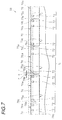
- Fig. 7 is a plan view which schematically shows a general LED module, and shows rectangular chips 70 constituting the LED module and the periphery thereof.
- Each of the rectangular chips 70 has a first aide surface 70a, a second side surface 70b, a third side surface 70c and a fourth side surface 70d.
- each chip 70 has plural light emitting elements 72 which are arranged on the chip so as to be linearly aligned in a longitudinal direction of the chip and displaced (offset) from the longitudinal center line of the chip to one side of the chip.
- the first side surface 70a is defined as one side surface of the chip 70 at which the light emitting elements 72 are arranged so as to be displaced (offset)
- the second side surface 70b is defined as another side surface of the chip 70 which intersects to the first side surface 70a
- the third side surface 70c is defined as another side surface of the chip 70 which is opposed to the first side surface 70a
- the fourth side surface 70d is defined as the residual side surface of the chip 70 which is located between the first side surface 70a and the third side surface 70c and intersects to both the first and third side surfaces 70a and 70c, that is, opposed to the second side surface 70b.
- all the plural light emitting elements 72 of each chip 70 having a substantially rectangular shape in plan view are disposed so as to be displaced (offset) from the center line of the chip 70 and located near to one side surface of the chip 70 (for example, the first side surface 70a), and also so as to be linearly aligned with one another.
- the chips 70 are arranged at a predetermined chip interval on a board 74 so that an array line L is formed by the plural light emitting elements 72 placed on all the chips 70.
- the chips 70 are arranged on the board 74 so that the first side surface 70a of each chip 70 is located at one side area with respect to the array line L while the third side surface 70c of each chip 70 is located at the other side area with respect to the array line L (i.e., the first side surface 70a and the third side surface 70c are located at opposite sides with respect to the array line L as the boundary between both the side areas).
- the chips are arranged on the board so that the side surfaces of the neighboring chips are confronted to each other over the entire width of the side surface of the chips, that is, the chips are arranged so as to be completely aligned with one another in the longitudinal direction of the chips as shown in Fig. 7. Therefore, during the mount/demount process in which a chip is disposed at a predetermined position or a defective chip is removed from the board, there is a risk that the chip concerned would come into careless contact with neighboring chips to disturb the arrangement of the chips or damage the neighboring chips.
- r represents the chip edge margin
- s represents the inter-chip distance.
- the following table shows the possible maximum inter-chip distance s for the chip edge margins of 4 ⁇ m and 8 ⁇ m when the resolution of the LED module is set to 400DPI, 600DPI, 1200DPI and 2400DPI.
- the probability that the arrangement of the neighboring chips is disturbed or the neighboring chips are damaged is more increased when a chip is disposed at a predetermined position or a defective chip is removed.
- the probability that the arrangement of the neighboring chips is disturbed or the neighboring chips are damaged is also more increased.
- the present invention has an object to provide a light emitting element module which can readily and quickly perform a process for arranging a chip at a predetermined position and a process for replacing a defective chip with a new chip even when the light emitting elements are arranged in high density (for example, 400 to 2400DPI) on each chip of the light emitting element module (for example, LED module).
- a light emitting element module which can readily and quickly perform a process for arranging a chip at a predetermined position and a process for replacing a defective chip with a new chip even when the light emitting elements are arranged in high density (for example, 400 to 2400DPI) on each chip of the light emitting element module (for example, LED module).
- the presents invention has another object to provide a light emitting element module and chips used for the light emitting element module, which can effectively prevent the printing characteristics from being deteriorated due to leakage of the light from the chip edge side surface even when the array of the light emitting elements of the light emitting element module is highly densified, and allow the margin of the inter-chip distance to be large.
- a light emitting element module having plural chips arranged on a board, each chip having plural light emitting elements, is characterized in that the plural light emitting elements are arranged on each chip so as to be displaced from the center line of the chip to one side surface of the chip (this one side surface is hereinafter referred to as "first side surface"), that is, the light emitting elements are located in the vicinity of the first side surface of the chip, and also arranged along the first side surface of the chip, and also that the plural chips are arranged on the board so that at least two neighboring chips are displaced (offset) from each other to the opposite sides (right and left sides) with respect to the alignment of the light emitting elements thereof (i.e., the chips are in a staggered arrangement).
- the plural chips are arranged such that the light emitting elements on all the chips form one arrangement line (i.e., the light emitting elements are arranged in straight alignment with one another), and at least two neighboring chips are displaced from each other to the opposite sides (right and left sides) with respect to the straight alignment of the light emitting elements so that the facing side surface of the neighboring chips are partially overlapped with each other in the alignment direction of the light emitting elements.
- the light emitting elements on the chips are straightforward aligned with one another to form substantially one arrangement line, so that the light emitting element module can implement a high-precision fight emitting function.
- the neighboring chips are arranged so as to be displaced from each other at least one position in the alignment direction of the light emitting elements, that is, there is provided at least one portion where the overlap area between the side surfaces of the neighboring chips is reduced, thereby enlarging the working space.
- the enlargement of the working space makes it possible to reduce the probability that the arrangement of neighboring chips is disturbed or neighboring chips are damaged when a chip is mounted at a predetermined position or a defective chip is replaced with a new one even when the arrangement of the light emitting elements is densified. Accordingly, the process of mounting at a predetermined position a chip having light emitting elements arranged in high density, and the process of replacing a defective chip with a new chip can be readily and quickly performed.
- the present invention it is sufficient to provide at least one position where the overlap area between the side surfaces of neighboring chips is reduced (i.e., at least two neighboring chips which are displaced from each other to the opposite directions). This is because even when there is provided only one position where the overlap area between the side surfaces of the neighboring chips is reduced, the provision of such a position can enlarge the working space by the amount corresponding to the reduced area, so that the mount process of chips and the replacement process of defective chips can be readily and quickly performed.
- the light emitting element module is defined as a module which is constructed by arranging plural chips each having plural densified light emitting elements (i.e., light emitting element array) on a board.
- the light emitting element is defined as an element for emitting/detecting light in the vertical direction to the surface of the board.
- the first side surface of the chip is one of the four side surfaces which define a chip having a rectangular shape in plan view, and it means one side surface of the chip to which the light emitting elements are located aside. Accordingly, when the planar shape of the chip is rectangular or parallelogrammatic, the first side surface of this chip corresponds to one of two longer sides of the chip.
- the provision of the light emitting elements in the vicinity of the first side surface means that the location (position) at which the light emitting elements are disposed is nearer to the first side surface. More specifically, the provision of the light emitting elements in the vicinity of the first side surface means that the light emitting elements are not brought into contact with the first side surface (that is, the surfaces of the light emitting elements and the first side surface are not on the same plane), and are disposed at a position (within a range) nearer to the first side surface of the chip than the longitudinal center line of the chip (for example, located at 350 ⁇ m from the first side surface of the chip) when the chip (the length of the second side surface intersecting to the first side surface, for example, 700 ⁇ m) is bisected along the arrangement line formed by the light emitting elements.
- the margin is set to a value in the range of about 1 to 100 ⁇ m, and optimally the margin is set to a value in the range of about 3 to 10 ⁇ m.
- the respective chips are alternately displaced (offset) to the opposite sides with respect to the longitudinal center line of the chips from one another on the board so that constant regularity is established in the arrangement. That is, the even-numbered chips are displaced (offset) to the one side surfaces (for example, the first side surfaces) thereof while the odd-numbered chips are displaced (offset) to the opposing side surfaces (for example, the third side surfaces) thereof so that the light emitting elements on the every chips are arranged in a straight line on the board.
- the overlap area between the second side surface (or the fourth side surface) of the odd-numbered chip and the second side surface (or the fourth side surface) of the even-numbered chip adjacent thereto is reduced, thereby enlarging the working space. Since the arranged chips are alternately and regularly displaced from one another as described above, there can be reduced the probability that the arrangement of the neighboring chips is disturbed or the neighboring chips are damaged when a chip is disposed at a predetermined position or a defective chip is replaced with a new one.
- the respective light emitting elements form one arrangement line as a whole, and the first side surfaces of the odd-numbered chips from the edge of the chip alignment are located in one side area of the board with respect to the arrangement line while the first side surfaces of the even-numbered chips from the edge of the chip alignment are located in the other side area of the board with respect to the arrangement line.
- the light emitting element module With the above-described construction of the light emitting element module, a more uniform arrangement line can be constructed by the light emitting element module. Therefore, when the light emitting element module as described above is applied to an LED printer head or the like, the light emitting element module exerts its print function with high precision. In addition, the overlap area between the second side surface (or the four side surface) of each odd-numbered chip and the fourth side surface (or the second side surface) of each even-numbered chip can be surely reduced, resulting in enlargement of the working space.
- the second side surface of the chip intersects to the first side surface at an angle other than 90° (not at the right angle).
- the margin (distance) between neighboring chips can be increased.
- the planar shape of each of said light emitting elements is set to a substantially parallelogram shape (containing no rectangular shape).
- the margin (distance) between neighboring chips can be certainly increased.
- the planar shape of the chips is substantially parallelogrammatic (containing no rectangle).
- the planar shape of the light emitting elements of the chips is substantially parallelogrammatic.
- each chip and the side surface of each light emitting element are preferably set to be substantially parallel to each other.
- each chip and the side surface of each light emitting element in the light emitting element module are matched with each other in shape as described above, thereby further increasing the distance from the side surface (at the edge side of the chip) of a light emitting element located at the edge portion of a chip to the second side surface (or fourth side surface) of the chip.
- the light emitting elements of the chips are preferably composed of LEDs (Light Emitting Diodes). This is because although the LED is small in dimension, it has a large light emission amount, and thus it is suitable for the light emitting element module.
- LEDs Light Emitting Diodes
- each of the light emitting elements of the chips has both a light emitting function (i.e., acts as a light emitter) and a photosensing (light receiving) function (i.e., acts as a photodetector).
- a light emitting function i.e., acts as a light emitter
- a photosensing (light receiving) function i.e., acts as a photodetector
- each light emitting element has both the light emitting function and the photosensing function as described above, when it is applied to an LED printer head or the like, there can be provided a reading/writing head for which the mount process for mounting a chip having light emitting elements and a repairing process for repairing a chip can be readily performed.
- each of the light emitting elements of the chips preferably performs the switching operation between the light emitting function and the photosensing function thereof by changing the applying direction of a bias voltage to the light emitting element (i.e., by selectively applying the bias voltage forwardly or reversely).
- both the light emitting function and the photosensing function can be readily provided to the light emitting element module of the present invention, no special device is needed and the light emitting element module can be designed in compact size.
- the light emitting element module of the present invention is preferably used as a light source for an LED printer head.
- the light emitting elements can be arranged in high density on the chips, and the chips having the highly-densified light emitting elements can be readily mounted on the board, so that the manufacturing process of LED printer heads is facilitated.
- the chip mount process for mounting a chip at a predetermined position and the chip replacement process for replacing a defective chip with a new one in a manufacturing or repairing process of a light source of a high-density LED printer head can be readily and quickly performed.
- the light emitting element module of the present invention is preferably used as a print head or a reading/writing head for an LED printer head.
- the light emitting element module of the present invention is suitably used as a printing head or a reading/writing head for an LED printer head because the light emitting elements can be designed in high density, the manufacturing process of the light emitting element module itself is easy, and each of the light emitting elements can be provided with both the light emitting function and the photosensing function.
- a chip having plural light emitting elements is characterized in that when one side surface of the chip is referred to as a first side surface and another side surface of the chip which intersects to the first side surface is referred to a second side surface, the light emitting elements are provided in the vicinity of the first side surface of the chip so as to be located along and aside to the first side surface of the chip, and the second side surface of the chip intersects to the first side surface thereof at an angle other than 90°.
- a plurality of chips thus constructed are arranged so as to be alternately displaced from one another, for example, they are disposed in a staggered arrangement so that the highly densely packed light emitting elements form one arrangement line (i.e., the light emitting elements are arranged in a straight alignment with one another), and the odd-numbered chips and the even-numbered chips from the edge of the chip alignment are arranged so that the facing side surface of these chips are partially overlapped in the chip alignment direction. That is, the light emitting element module which has an enlarged working space and is provided with highly densely packed light emitting elements can be constructed by using the above chips.
- the chip mount process for mounting a chip at a predetermined position and the chip replacement process for replacing a defective chip with a new one can be readily and quickly performed.
- the chip of the present invention is designed to be substantially parallelogram (containing no rectangle) in plan view.
- the margin of the inter-chip distance is longer than the case where the second side surface of each chip intersects to the first side surface thereof vertically.
- the mount degree of each chip on the board is enhanced, resulting in facilitation of the chip mount process and the chip replacement process.
- the light emitting elements of the chip are designed to be substantially parallelogrammatic (containing no rectangular shape) in plan view.
- the shape of the light emitting elements of the chip as described above, the distance from the side surface (at the edge side of the chip) of the light emitting element located at the edge portion of each chip to the second side surface (or fourth side surface) of the chip can be increased.
- the distance from the side surface (at the edge side of the chip) of the light emitting element located at the edge portion of each chip to the second side surface (or fourth side surface) of the chip can be more increased.
- each light emitting element of the chip is provided with both the light emitting function and the photosensing (photodetecting) function.
- the chip when the chip is applied to an LED printer head or the like, there can be provided a reading and writing head for which the manufacturing process and the repairing process can be readily performed.
- each light emitting element of the chip performs the switching operation between the light emitting function and the photosensing function by changing the bias-voltage applying direction in the chip.
- the light emitting element module of the present invention can be readily provided with both the light emitting function and the photosensing function with no special device, and also the light emitting element module can be miniaturized.
- LED module LED printer head
- LED printer head which is one type of light emitting element modules
- an embodiment of a chip will be also described together in a second embodiment.
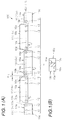
- Figs. 1(A) and 1(B) show an LED module (LED printer head) of a first embodiment according to the present invention.
- Fig. 1(A) is a plan view showing the LED module, and also shows a chip serving as a part constituting the LED module and the periphery thereof and Fig. 1(B) is a side view showing the LED module which is taken in the direction of S in Fig. 1(A).
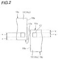
- Fig. 2 is an enlarged view showing a part which is surrounded by a one-dotted broken line in Fig. 1(A), and
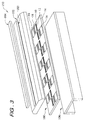
- Fig. 3 is an exploded view when the LED module shown in Figs. 1 and Fig. 2 is used as a part of an LED printer head.
- electrodes, a board, etc. are omitted from the illustration of the LED module.
- a generally-used rectangular chip for example, 700 ⁇ m in longitudinal direction (the length of the second and the fourth side surfaces), 8000 ⁇ m in lateral direction (the length of the first and third side surfaces), 300 ⁇ m in height
- 700 ⁇ m in longitudinal direction the length of the second and the fourth side surfaces
- 8000 ⁇ m in lateral direction the length of the first and third side surfaces
- 300 ⁇ m in height is used.
- each chip 10 is provided with plural light emitting elements 12 which are arrayed in high density. All the light emitting elements 12 are arranged aside in the vicinity of the first side surfaces 10a of the chips so as to be in straight alignment with one another along the first side surfaces 10a.
- Each chip 10 comprises the first side surface 10a, the second side surface 10b, the third side surface 10c and the fourth side surface 10d.
- first side surface 10a one side surface of each chip along which the light emitting elements 12 are located is referred to as a first side surface 10a.
- second side surface 10b another side surface of each chip which intersects to the first side surface 10a is referred to as a second side surface 10b.
- third side surface 10c Another side surface of each chip which is opposed to the first side surface 10a is referred to as a third side surface 10c, and the residual side surface of each chip which is opposed to the second side surface 10b is referred to as a fourth side surface 10d.
- the chips 10 are arranged (disposed) so that the distance between the neighboring chips 10 (the inter-chip distance) d 1 is fixed.
- the chips 10 are arranged (disposed) on the board so that the neighboring chips arc alternately displaced (offset) from each other (i.e., the chips are disposed in a staggered arrangement) and the plural light emitting elements 12 provided to the respective chips 10 are aligned with one another to form an arrangement line L (a row of the light emitting elements 12).
- one half group of chips which contain the leftmost chip and subsequent every other chips from the left edge of the chip alignment are set as odd-numbered chips 10x as shown in Fig. 1(A).
- the other half group which contain the second chip from the left side and subsequent every other chips are set as even-numbered chips 10y as shown in Fig. 1(B).
- the first side surfaces 10a of the odd-numbered chips 10x are located in one side area with respect to the arrangement line L of the light emitting elements 12 (in Fig. 1(A), the upper side area of the arrangement line L of the light emitting elements), and the first side surfaces 10a of the even-numbered chips 10y are located in the other side area with respect to the arrangement line L of the light emitting elements 12 (in Fig. 1(A), the lower side area of the arrangement line L of the light emitting elements).
- the odd-numbered chips 10x and the even-numbered chips 10y are arranged so as to be offset in the opposite directions with respect to the arrangement line L of the light emitting elements 12. That is, the direction from the first side surface 10a to the third side surface 10c is opposite between the odd-numbered chips 10x and the even-numbered chips 10y.
- the side surface of the LED module 100 is viewed along the extension line of the arrangement line L of the light emitting elements 12, each odd-numbered chip 10x and each even-numbered chip 10y are partially overlapped with each other as shown in Fig. 1(B) (the overlap area between the odd-numbered chip 10x and the even-numbered chip 10y is hatched in Fig. 1(B). That is, the chips are partially overlapped with each other between the first side surface 10a of each odd-numbered chip 10x and the first side surface 10a of each even-numbered chip 10y.
- the reduction of the overlap area between the neighboring chips as described above enables the working space to be enlarged. Accordingly, there can be eliminated portions at which the disturbance of the arrangement of the neighboring chips or the damage of the neighboring chips can be suppressed even when a chip is mounted at a predetermined position on a board or a defective chip is replaced with a new one.
- the chip mount process for mounting a chip at a predetermined position and the chip replacement process for replacing a defective chip with a new one can be readily and quickly performed.
- the chip has a rectangular parallelepiped body having the size of 700 ⁇ m in longitudinal direction, 8000 ⁇ m in lateral direction and 300 ⁇ m in height, and the light emitting elements are linearly aligned with one another along the side surface (first side surface 10a) of 8000 ⁇ m x 300m ⁇ in dimension on the surface of the chip having the size of 700 ⁇ m x 8000 ⁇ m.
- the light emitting elements are linearly aligned with one another, however, the light emitting elements may be arranged on two or more rows. This arrangement is preferable because the area of the light emitting elements is larger as a whole.
- each light emitting element 12 is a square whose side length is equal to 8 ⁇ m as shown in Fig. 2, and the distance y from the first side surface 10a to each light emitting element 12 is set to 6 ⁇ m.
- the overlap area between the neighboring chips can be reduced to 1/35 of that of the prior art in which the chips are arranged so that the side surfaces thereof are overlapped with one another over the full width thereof.
- the ratio of the overlap portion is preferably set to 50% or less at maximum, more preferably 25% or less, and optimally 5% or less.
- the overlap area between the neighboring chips is set to a value within the above range, the working space can be enlarged. Accordingly, even when the light emitting elements are arranged in a high density in the LED module 100, the chips 10 can be successively readily and quickly arranged on the board 14 by a die-bonding technique or the like. Further, the chip mount process and the chip replacing (the chip repairing) process can be also readily and quickly performed.
- Fig. 3 is an exploded view showing an LED printer head 110 when the LED module 100 is used as a part of the LED printer head 110 as shown in Figs. 1 and 2.
- the LED printer head 110 comprises a support portion 106, an LED module 100, a rod lens array holder 102 and a rod lens array 104 from the lower side.
- the support portion 106 serves to mechanically hold the LED module 100, and also serves as a heat sink for radiating heat which occurs in the LED module 100.
- the rod lens array holder 102 is directly provided at the upper side of the LED module 100 to accurately position the rod lens array 104 which is mounted in the opening 103 of the holder 102.
- the rod lens array 104 serves to efficiently focus an LED image onto a photosensitive member.
- the LED module 100 uses the chips each having the light emitting elements 12 which are located aside to the first side surface 10a of the chip 10 and on the surface of the chip, and arranged along the first side surface 10a.
- a plurality of these chips 10 are arranged on the board 14 while alternately displaced (offset) from one another (in a staggered arrangement).
- an IC driver 16 for driving a chip is provided on the board 14 of the LED module 100 in association with each chip.
- Each light emitting element 12 on the surface of each chip 10 is electrically connected to each terminal of the IC driver 16 by a bonding wire 18. Accordingly, in the LED printer head 110 thus constructed, each IC driver 16 controls each light emitting element 12 to exhibit its light emitting function, and data are printed on a photosensitive member through the rod lens array 104.
- the LED module 100 which constitutes a part of the LED printer head 110
- the overlap area between the neighboring chips 10 is reduced, and the working space is enlarged. Accordingly, when the LED printer head 110 is constructed, a highly densified (for example, 400 to 2400DPI) chip 10 can be readily and quickly mounted at a predetermined position. In addition, even when a defective chip occurs due to use of the LED printer head 110, the chip can be readily and quickly replaced with a new one.
- a highly densified (for example, 400 to 2400DPI) chip 10 can be readily and quickly mounted at a predetermined position.
- the chip can be readily and quickly replaced with a new one.
- Figs. 4(A) and 4(B) , Fig. 5 and Fig. 6 show an LED module according to a second embodiment of the present invention.
- Fig. 4(A) is a schematic plan view showing the LED module, and shows a chip constituting a part of the LED module and the periphery thereof.
- Fig. 4(A) is a side view showing the LED module, which is viewed from the direction of S in Fig. 4(A).
- Fig. 5 is an enlarged view showing a part surrounded by a one-dotted broken line in Fig. 4(A).
- Fig. 6 is a schematic diagram to show the comparison result between the inter-chip distance of the LED module of the second embodiment and the inter-chip distance of the LED module of the first embodiment.
- electrodes, a board, etc. are omitted from the illustration.
- each chip 50 is provided with plural light emitting elements 52 which are arranged in high density, and the light emitting elements 52 are located aside to the first side surfaces 50a of all the chips 50 and linearly aligned with one another along the first side surfaces 50a.
- the side surface of each chip 50 which intersects to the first side surface of the chip, that is, the second side surface 50b which faces the adjacent chip is set to intersect to the first side surface 50a at an angle other than 90°. Accordingly, the second side surface 50b serves as the chip edge which faces the adjacent chip.
- the inter-chip distance is maximum second side surface 50b when the intersection angle ⁇ between the second side surface 50b and the first side surface 50a is equal to 60°.
- the second embodiment will be described on the assumption that the second side surface 50b intersects to the first side surface 50a at an angle ⁇ of 60°.
- the light emitting element which is located nearest to the second side surface 50b of each chip 50 (hereinafter referred to as "chip edge light emitting element") is designed in a parallelogram shape in plan view, and the outline (contour) of the chip edge light emitting element 52 at the second side surface 50b side is parallel to the second side surface 50b.
- the planar shape of the chip edge light emitting element 52 is set to be parallelogrammatic (excluding rectangle), however, it is not limited to the parallelogrammatic shape.
- the planar shape may be triangular, trapezoidal, semi-circular or the like insofar as the second side surface (outline) of the chip edge light emitting element is parallel to the second side surface (outline) of the chip.
- the planar shape of the light emitting element is set to a shape other than the square and the rectangle, the minimum square or rectangle in which the light emitting element is accommodated (one side of the square or the rectangle must be parallel to the first side surface is assumed, and the dot pitch from the intersection point between the diagonal lines of the square or the rectangle to the adjacent light emitting element is measured.
- the chips 50 are disposed on the board 54 so that the inter-chip distance d 2 is constant, and also these chips 50 are arranged on the board so that the arrangement line L (the array of the light emitting elements 52) is formed by plural light emitting elements 52 which are provided to the chips 50 (i.e., the plural light emitting elements are linearly aligned with one another to form the arrangement line L).
- the leftmost chip and subsequent every other chips from the leftmost chip are set as odd-numbered chips 50x while the second chip from the left edge of the chip alignment and subsequent every other chips are set as even-numbered chips 50y.
- the first side surfaces 50a of the odd-numbered chips 50x are located in one side area with respect to the arrangement line L of the light emitting elements 52 on the board (print circuit board) 54 (the upper side area of the arrangement line L of the light emitting elements 52 in Fig. 4(A)). Further, the first side surfaces 50a of the even-numbered chips 50y are located in the other side area with respect to the arrangement line L of the light emitting element 52 on the board 54 (the lower side area of the arrangement line L of the light emitting elements 52 in Fig. 4(A)).
- each odd-numbered chip 50x and each even-numbered chip 50y are partially overlapped with each other when the side surface of the LED module 60 is viewed along the extension line of the arrangement line L of the light emitting elements 50 (in Fig. 4(B), the overlap area between the odd-numbered chip 50x and the even-numbered chip 50y is hatched).
- This arrangement would be readily understandable from the enlarged view (Fig. 5) of a portion which is surrounded by one-dotted broken line in Fig. 4(A). That is, with respect to the odd-numbered chip 50x and the even-numbered chip 50y which are adjacent to each other, as shown in Fig.
- the second side surface 50b of the odd-numbered chip 50x and the second side surface 50b of the even-numbered chip 50y are partially overlapped with each other.
- the length of the second side surface 50b of the odd-numbered chip 50x (the second side surface 50b of the even-numbered chip 50y has the same length) is assumed as 100%, the overlap area between the neighboring chips corresponds to about 44%.
- the process for mounting a chip at a predetermined position and the process for replacing a defective chip with a new chip can be readily and quickly performed.
- Fig. 6 shows the peripheries of the chip edges of two chips which are adjacent to each other in the LED module of the second embodiment, and also illustrates, with one dotted broken line, the LED module 60 of the second embodiment while superposing the LED module 60 of the second embodiment with the LED module 100 of the first embodiment under the condition of the same distance y from the first side surface 50a to the light emitting elements 52, the same chip edge margin z and the y same dot pitch p . That is, the illustrations of Figs. 2 and 5 are shown while overlapped with each other, and also Fig. 2 is illustrated by one-dotted broken line.
- Fig. 6 shows the case where the distance y from the first side surface to the light emitting elements is set to 6 ⁇ m, the chip edge margin z is set to 4 ⁇ m, and the dot pitch p is set to 21 ⁇ m.
- the light emitting element is designed as a square having one side of 8 ⁇ m, and the inter-chip distance d 1 is set to 5 ⁇ m.
- each side x of the minimum square in which the light emitting element is accommodated is set to 8 ⁇ m. Since the second side surface 50b intersects to the first side surface 50a at an angle ⁇ of 60° in the LED module 60 of the second embodiment, the inter-chip distance d 2 is equal to 7.2 ⁇ m.
- the margin of the inter-chip distance is increased by about 1.4 times as compared with the first embodiment in which the side surface of the chip which faces the adjacent chip intersects to the first side surface at the right angle.
- the LED module 60 of the second embodiment is also usable as a part of an LED printer head. That is, as described on the first embodiment (see Fig. 3), the LED printer head can be constructed by the LED module 60 of the second embodiment, the support member, the rod lens array holder and the rod lens array.
- each IC driver controls each light emitting element to exhibit its light emitting function, whereby print can be performed on a photosensitive member through the rod lens array.
- each of the above-described embodiments relates to an LED module which is mainly applied to an LED print head or the like.
- the present invention may be applied to an image sensor or the like which is constructed by arranging on a board chips each including plural PDs (photodiodes) as light emitting elements.
- the light emitting elements are controlled to selectively exhibit one of the light emitting function and the photosensing function by switching the application direction of a bias voltage to chips, whereby the LED module can be applied to not only an LED printer head for print (exhibiting a print function), but also a reading head for reading information from a printed medium or the like, or a reading/writing LED print head.
- the light emitting element module is constructed by arranging on a board chips each of which comprises plural light emitting elements, and when one of the side surfaces of each chip is expressed as a first side surface, the respective light emitting elements are provided on each chip so as to be located aside to the first side surface of the chip, and the light emitting elements are arranged along the first side surface of the chip.
- the respective chips are arranged on the board so that one arrangement line is formed by the light emitting elements on all the chips, and the first side surfaces of the odd-numbered chips are located in one side area with respect to the arrangement line of the light emitting elements while the first side surfaces of the even-numbered chips are located in the other side area with respect to the arrangement line of the light emitting elements.
- each odd-numbered chip and each even-numbered chip are partially overlapped with each other when viewing the side surface of the light emitting element module along the extension line of the arrangement line of the light emitting elements. That is, the odd-numbered chip and the even-numbered chip are overlapped with each other only between the first side surface of the odd-numbered chip and the first side surface of the even-numbered chip, and the neighboring chips are aligned so that the side surfaces of the chips are partially confronted to each other (i.e., they are confronted to each other only at a narrow portion extending from the alignment of the light emitting elements to the first side surface.
- the reduction of the overlap area between the neighboring chips as described above makes it possible to reduce the probability that when a chip is mounted at a predetermined position on the board or a defective chip is replaced with a new one, the arrangement of the adjacent chips would be disturbed or the adjacent chips would be damaged. That is, the process for mounting at a predetermined position a chip having light emitting elements which are arranged in high density, and the process for replacing a defective chip with a new one can be readily and quickly performed.
- the confronting second side surfaces of the adjacent chips are set to intersect to the first side surfaces thereof at an angle other than 90° (not at the right angle).
- the light emitting element chip edge light emitting element which is nearest to the second side surface of each chip is set to be parallel to the second side surface. Accordingly, under the condition that the chip edge margin is fixed, the margin of the inter-chip distance is increased to a larger value as compared with the case where the second side surfaces of the adjacent chips which are confronted to each other are set to intersect to the first side surfaces thereof at the right angle.
- the margin of the inter-chip distance is increased, the working space is enlarged, and the freedom of the chip mount on the board is enhanced. That is, a chip having plural light emitting elements which are arranged in high density can be more easily arranged with high precision.
Landscapes
- Physics & Mathematics (AREA)
- Optics & Photonics (AREA)
- Health & Medical Sciences (AREA)
- General Health & Medical Sciences (AREA)
- Toxicology (AREA)
- Led Device Packages (AREA)
- Printers Or Recording Devices Using Electromagnetic And Radiation Means (AREA)
- Led Devices (AREA)
Priority Applications (2)
| Application Number | Priority Date | Filing Date | Title |
|---|---|---|---|
| JP9812596A JPH09283808A (ja) | 1996-04-19 | 1996-04-19 | 受発光素子モジュール及びチップ |
| EP97116111A EP0908953A1 (fr) | 1996-04-19 | 1997-09-16 | Module à élément électroluminescent et puce |
Applications Claiming Priority (2)
| Application Number | Priority Date | Filing Date | Title |
|---|---|---|---|
| JP9812596A JPH09283808A (ja) | 1996-04-19 | 1996-04-19 | 受発光素子モジュール及びチップ |
| EP97116111A EP0908953A1 (fr) | 1996-04-19 | 1997-09-16 | Module à élément électroluminescent et puce |
Publications (1)
| Publication Number | Publication Date |
|---|---|
| EP0908953A1 true EP0908953A1 (fr) | 1999-04-14 |
Family
ID=26145782
Family Applications (1)
| Application Number | Title | Priority Date | Filing Date |
|---|---|---|---|
| EP97116111A Withdrawn EP0908953A1 (fr) | 1996-04-19 | 1997-09-16 | Module à élément électroluminescent et puce |
Country Status (2)
| Country | Link |
|---|---|
| EP (1) | EP0908953A1 (fr) |
| JP (1) | JPH09283808A (fr) |
Cited By (1)
| Publication number | Priority date | Publication date | Assignee | Title |
|---|---|---|---|---|
| EP1059171A1 (fr) * | 1999-06-10 | 2000-12-13 | Canon Kabushiki Kaisha | Réseaux de lentilles barreaux et tête d'imprimante et imprimante optique les utilisant |
Families Citing this family (4)
| Publication number | Priority date | Publication date | Assignee | Title |
|---|---|---|---|---|
| JP4092824B2 (ja) | 1999-09-21 | 2008-05-28 | 富士ゼロックス株式会社 | 自己走査型発光素子アレイチップの配列方法 |
| JP5061959B2 (ja) * | 2008-03-03 | 2012-10-31 | セイコーエプソン株式会社 | 記録装置および流体噴射装置 |
| TWI781193B (zh) * | 2017-08-24 | 2022-10-21 | 日商索尼股份有限公司 | 發光模組、光源單元、光造形裝置 |
| US11710942B2 (en) | 2017-12-13 | 2023-07-25 | Sony Corporation | Method of manufacturing light-emitting module, light-emitting module, and device |
Citations (6)
| Publication number | Priority date | Publication date | Assignee | Title |
|---|---|---|---|---|
| FR2420848A1 (fr) * | 1978-03-23 | 1979-10-19 | Commissariat Energie Atomique | Procede de realisation de diodes electroluminescentes et photodetectrices |
| JPS58125879A (ja) * | 1982-01-21 | 1983-07-27 | Matsushita Electric Ind Co Ltd | 固体素子アレイの製造方法 |
| EP0097261A2 (fr) * | 1982-06-19 | 1984-01-04 | AEG Olympia Aktiengesellschaft | Imprimante à tête d'impression optique pour l'enregistrement par lignes d'informations de graphiques et de textes |
| EP0319907A2 (fr) * | 1987-12-09 | 1989-06-14 | Hitachi Cable, Ltd. | Plaquette avec matrice de diodes éléctroluminescentes et méthode de fabrication |
| JPH0260767A (ja) * | 1988-08-26 | 1990-03-01 | Nec Corp | 電子写真式プリンタ用ledヘッド |
| JPH0299350A (ja) * | 1988-10-07 | 1990-04-11 | Nec Corp | Ledヘッド |
-
1996
- 1996-04-19 JP JP9812596A patent/JPH09283808A/ja not_active Withdrawn
-
1997
- 1997-09-16 EP EP97116111A patent/EP0908953A1/fr not_active Withdrawn
Patent Citations (6)
| Publication number | Priority date | Publication date | Assignee | Title |
|---|---|---|---|---|
| FR2420848A1 (fr) * | 1978-03-23 | 1979-10-19 | Commissariat Energie Atomique | Procede de realisation de diodes electroluminescentes et photodetectrices |
| JPS58125879A (ja) * | 1982-01-21 | 1983-07-27 | Matsushita Electric Ind Co Ltd | 固体素子アレイの製造方法 |
| EP0097261A2 (fr) * | 1982-06-19 | 1984-01-04 | AEG Olympia Aktiengesellschaft | Imprimante à tête d'impression optique pour l'enregistrement par lignes d'informations de graphiques et de textes |
| EP0319907A2 (fr) * | 1987-12-09 | 1989-06-14 | Hitachi Cable, Ltd. | Plaquette avec matrice de diodes éléctroluminescentes et méthode de fabrication |
| JPH0260767A (ja) * | 1988-08-26 | 1990-03-01 | Nec Corp | 電子写真式プリンタ用ledヘッド |
| JPH0299350A (ja) * | 1988-10-07 | 1990-04-11 | Nec Corp | Ledヘッド |
Non-Patent Citations (3)
| Title |
|---|
| PATENT ABSTRACTS OF JAPAN vol. 007, no. 236 (E - 205) 20 October 1983 (1983-10-20) * |
| PATENT ABSTRACTS OF JAPAN vol. 014, no. 231 (M - 0974) 16 May 1990 (1990-05-16) * |
| PATENT ABSTRACTS OF JAPAN vol. 014, no. 305 (M - 0992) 29 June 1990 (1990-06-29) * |
Cited By (3)
| Publication number | Priority date | Publication date | Assignee | Title |
|---|---|---|---|---|
| EP1059171A1 (fr) * | 1999-06-10 | 2000-12-13 | Canon Kabushiki Kaisha | Réseaux de lentilles barreaux et tête d'imprimante et imprimante optique les utilisant |
| US6473111B1 (en) | 1999-06-10 | 2002-10-29 | Canon Kabushiki Kaisha | Rod lens array and printer head and optical printer using the same |
| US6788329B2 (en) | 1999-06-10 | 2004-09-07 | Canon Kabushiki Kaisha | Rod lens array and printer head and optical printer using the same |
Also Published As
| Publication number | Publication date |
|---|---|
| JPH09283808A (ja) | 1997-10-31 |
Similar Documents
| Publication | Publication Date | Title |
|---|---|---|
| US6163036A (en) | Light emitting element module with a parallelogram-shaped chip and a staggered chip array | |
| EP0986103B1 (fr) | Module à éléments électroluminescents et tête d'impression l'utilisant | |
| EP0098382B1 (fr) | Illumination d'intensité uniforme par des lentilles en forme de barreau | |
| US6467870B2 (en) | Recording head | |
| EP0319907B1 (fr) | Plaquette avec matrice de diodes éléctroluminescentes et méthode de fabrication | |
| JP2510423B2 (ja) | 光情報書込み装置および光情報検出装置ならびにその光学レンズ系の構造 | |
| US8182069B2 (en) | Method for modular arrangement of a silicon based array and modular silicon based array | |
| KR100781910B1 (ko) | 광 프린터 헤드의 점등 방법 | |
| US20050151828A1 (en) | Xerographic printing system with VCSEL-micro-optic laser printbar | |
| US6448995B1 (en) | Image read/write head, and image processing apparatus incorporating the same | |
| CN104243756A (zh) | 图像传感器单元、图像读取装置以及图像形成装置 | |
| JP2002248803A (ja) | Ledプリントヘッド及びその調整方法 | |
| EP0468255A2 (fr) | Détecteur d'image linéaire du type à contact | |
| JP2000289250A (ja) | Ledアレイチップおよびledアレイプリントヘッド | |
| JPS62141763A (ja) | センサ・アレイの製造方法とアレイ | |
| JPS5912877A (ja) | 光プリンタ | |
| JPH09283808A (ja) | 受発光素子モジュール及びチップ | |
| JPH02212167A (ja) | Ledプリントヘッド | |
| JP2004209703A (ja) | 光書き込みヘッド | |
| JP2008227467A (ja) | 発光素子アレイチップおよび露光光源装置 | |
| JPH09283807A (ja) | 受発光素子モジュール | |
| US6677970B1 (en) | Light-emitting diode array and optical print head | |
| JPH07186444A (ja) | 画像装置 | |
| JPH08216448A (ja) | 自己走査型集積化発光素子アレイおよびこれを用いた発光装置 | |
| JPH08104030A (ja) | 画像装置 |
Legal Events
| Date | Code | Title | Description |
|---|---|---|---|
| PUAI | Public reference made under article 153(3) epc to a published international application that has entered the european phase |
Free format text: ORIGINAL CODE: 0009012 |
|
| AK | Designated contracting states |
Kind code of ref document: A1 Designated state(s): AT BE CH DE DK ES FI FR GB GR IE IT LI LU MC NL PT SE |
|
| AKX | Designation fees paid | ||
| STAA | Information on the status of an ep patent application or granted ep patent |
Free format text: STATUS: THE APPLICATION IS DEEMED TO BE WITHDRAWN |
|
| 18D | Application deemed to be withdrawn |
Effective date: 19991015 |
|
| REG | Reference to a national code |
Ref country code: DE Ref legal event code: 8566 |