EP0468255A2 - Détecteur d'image linéaire du type à contact - Google Patents
Détecteur d'image linéaire du type à contact Download PDFInfo
- Publication number
- EP0468255A2 EP0468255A2 EP91111233A EP91111233A EP0468255A2 EP 0468255 A2 EP0468255 A2 EP 0468255A2 EP 91111233 A EP91111233 A EP 91111233A EP 91111233 A EP91111233 A EP 91111233A EP 0468255 A2 EP0468255 A2 EP 0468255A2
- Authority
- EP
- European Patent Office
- Prior art keywords
- image sensor
- contact type
- pitch
- picture elements
- chip
- Prior art date
- Legal status (The legal status is an assumption and is not a legal conclusion. Google has not performed a legal analysis and makes no representation as to the accuracy of the status listed.)
- Withdrawn
Links
Images
Classifications
-
- H—ELECTRICITY
- H04—ELECTRIC COMMUNICATION TECHNIQUE
- H04N—PICTORIAL COMMUNICATION, e.g. TELEVISION
- H04N1/00—Scanning, transmission or reproduction of documents or the like, e.g. facsimile transmission; Details thereof
- H04N1/04—Scanning arrangements, i.e. arrangements for the displacement of active reading or reproducing elements relative to the original or reproducing medium, or vice versa
- H04N1/19—Scanning arrangements, i.e. arrangements for the displacement of active reading or reproducing elements relative to the original or reproducing medium, or vice versa using multi-element arrays
- H04N1/1903—Arrangements for enabling electronic abutment of lines or areas independently scanned by different elements of an array or by different arrays
-
- H—ELECTRICITY
- H04—ELECTRIC COMMUNICATION TECHNIQUE
- H04N—PICTORIAL COMMUNICATION, e.g. TELEVISION
- H04N1/00—Scanning, transmission or reproduction of documents or the like, e.g. facsimile transmission; Details thereof
- H04N1/04—Scanning arrangements, i.e. arrangements for the displacement of active reading or reproducing elements relative to the original or reproducing medium, or vice versa
- H04N1/19—Scanning arrangements, i.e. arrangements for the displacement of active reading or reproducing elements relative to the original or reproducing medium, or vice versa using multi-element arrays
- H04N1/191—Scanning arrangements, i.e. arrangements for the displacement of active reading or reproducing elements relative to the original or reproducing medium, or vice versa using multi-element arrays the array comprising a one-dimensional [1D] array
- H04N1/192—Simultaneously or substantially simultaneously scanning picture elements on one main scanning line
- H04N1/193—Simultaneously or substantially simultaneously scanning picture elements on one main scanning line using electrically scanned linear arrays, e.g. linear CCD arrays
- H04N1/1934—Combination of arrays
-
- H—ELECTRICITY
- H10—SEMICONDUCTOR DEVICES; ELECTRIC SOLID-STATE DEVICES NOT OTHERWISE PROVIDED FOR
- H10F—INORGANIC SEMICONDUCTOR DEVICES SENSITIVE TO INFRARED RADIATION, LIGHT, ELECTROMAGNETIC RADIATION OF SHORTER WAVELENGTH OR CORPUSCULAR RADIATION
- H10F39/00—Integrated devices, or assemblies of multiple devices, comprising at least one element covered by group H10F30/00, e.g. radiation detectors comprising photodiode arrays
- H10F39/10—Integrated devices
- H10F39/12—Image sensors
Definitions
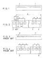
- the present invention relates to a linear image sensor of the contact type used in an image scanner and a facsimile machine etc.
- FIG. 3 is a plan view of an example of such contact type linear image sensor.
- a plurality of image sensor chips 21 are arranged linearly on a base plate 11.
- Fig. 4 shows a plan view of one image sensor chip 21.
- the chip 21 provided with a linear array of picture elements 31 arranged such that an end element is spaced an interval b from an inner adjacent element and the remaining intermediate elements are spaced an interval a from each other.
- the end interval b is set smaller than the intermediate interval a.
- the intermediate interval a is set exactly identical to a given standard reading pitch of the sensor in the horizontal or main scanning direction.
- a dimensional error of more or less one picture element order does not effect quality of a reproduced image in case of 16 dots/mm of the resolution.
- an actual arrangement pitch may be locally widened exceptionally at one or more intermediate spots, relative to the constant pitch value a' in view of optimum and efficient lead pattern layout.
- the constant pitch a' is maintained almost all of the picture elements including end ones, thereby maintaining uniform quality of a reproduced image.
- the present invention can be applied not only to an image sensor having a single line of picture elements, but also to those having multiple lines of picture elements.
Landscapes
- Engineering & Computer Science (AREA)
- Multimedia (AREA)
- Signal Processing (AREA)
- Facsimile Heads (AREA)
- Solid State Image Pick-Up Elements (AREA)
Applications Claiming Priority (2)
| Application Number | Priority Date | Filing Date | Title |
|---|---|---|---|
| JP2198286A JP3013189B2 (ja) | 1990-07-26 | 1990-07-26 | 密着型イメージセンサ |
| JP198286/90 | 1990-07-26 |
Publications (2)
| Publication Number | Publication Date |
|---|---|
| EP0468255A2 true EP0468255A2 (fr) | 1992-01-29 |
| EP0468255A3 EP0468255A3 (en) | 1992-03-11 |
Family
ID=16388598
Family Applications (1)
| Application Number | Title | Priority Date | Filing Date |
|---|---|---|---|
| EP19910111233 Withdrawn EP0468255A3 (en) | 1990-07-26 | 1991-07-05 | Linear image sensor of the contact type |
Country Status (6)
| Country | Link |
|---|---|
| US (1) | US5619345A (fr) |
| EP (1) | EP0468255A3 (fr) |
| JP (1) | JP3013189B2 (fr) |
| KR (1) | KR100212030B1 (fr) |
| CA (1) | CA2047930A1 (fr) |
| TW (1) | TW198768B (fr) |
Cited By (5)
| Publication number | Priority date | Publication date | Assignee | Title |
|---|---|---|---|---|
| DE4317945A1 (de) * | 1993-03-22 | 1994-09-29 | Paul Dr Debbage | Verfahren und Vorrichtung zur Untersuchung eines Objektes |
| DE4325724A1 (de) * | 1993-07-30 | 1995-02-02 | Paul Dr Debbage | Vorrichtung und Verfahren zur Untersuchung eines Objektes und zur Einwirkung auf das Objekt |
| EP0657938A1 (fr) * | 1993-12-06 | 1995-06-14 | Minnesota Mining And Manufacturing Company | Panneau détecteur de radiation à l'état solide comprenant des détecteurs photosensibles disposés les uns à côté des autres pour minimiser les effets de bord entre ceux-ci |
| EP0975143A3 (fr) * | 1998-07-22 | 2000-12-20 | Hewlett-Packard Company | Ensemble photosensible linéaire à plusieurs segments de lecture |
| EP1091558A4 (fr) * | 1998-01-30 | 2003-01-15 | Rohm Co Ltd | Microplaquette de detection d'image et dispositif de lecture d'image la comportant |
Families Citing this family (6)
| Publication number | Priority date | Publication date | Assignee | Title |
|---|---|---|---|---|
| US6556315B1 (en) | 1999-07-30 | 2003-04-29 | Hewlett-Packard Company | Digital image scanner with compensation for misalignment of photosensor array segments |
| JP2003143381A (ja) * | 2001-08-22 | 2003-05-16 | Canon Inc | 画像処理装置 |
| JP2003115984A (ja) * | 2001-10-05 | 2003-04-18 | Seiko Instruments Inc | 画像読み取り装置 |
| JP3829853B2 (ja) * | 2004-03-31 | 2006-10-04 | 三菱電機株式会社 | イメージセンサ |
| JP4179329B2 (ja) | 2006-03-17 | 2008-11-12 | セイコーエプソン株式会社 | ラインセンサチップ、ラインセンサ、画像情報読取装置、ファクシミリ、スキャナ及び複写機 |
| JP6822010B2 (ja) * | 2016-08-29 | 2021-01-27 | セイコーエプソン株式会社 | スキャナーおよび画像データの生成方法 |
Family Cites Families (5)
| Publication number | Priority date | Publication date | Assignee | Title |
|---|---|---|---|---|
| FR2110763A5 (fr) * | 1970-10-29 | 1972-06-02 | Comp Generale Electricite | |
| US4652743A (en) * | 1984-11-30 | 1987-03-24 | Brother Kogyo Kabushiki Kaisha | Optical image-reading apparatus |
| US4748516A (en) * | 1985-03-15 | 1988-05-31 | Brother Kogyo Kabushiki Kaisha | Input/output device for image reading and printing |
| US4692812A (en) * | 1985-03-26 | 1987-09-08 | Kabushiki Kaisha Toshiba | Picture image reader |
| JPH0287869A (ja) * | 1988-09-26 | 1990-03-28 | Ricoh Co Ltd | 千鳥配列マルチチツプ型イメージセンサ |
-
1990
- 1990-07-26 JP JP2198286A patent/JP3013189B2/ja not_active Expired - Lifetime
-
1991
- 1991-07-02 TW TW080105140A patent/TW198768B/zh not_active IP Right Cessation
- 1991-07-05 EP EP19910111233 patent/EP0468255A3/en not_active Withdrawn
- 1991-07-15 KR KR1019910012069A patent/KR100212030B1/ko not_active Expired - Lifetime
- 1991-07-16 US US07/731,741 patent/US5619345A/en not_active Expired - Lifetime
- 1991-07-25 CA CA002047930A patent/CA2047930A1/fr not_active Abandoned
Cited By (5)
| Publication number | Priority date | Publication date | Assignee | Title |
|---|---|---|---|---|
| DE4317945A1 (de) * | 1993-03-22 | 1994-09-29 | Paul Dr Debbage | Verfahren und Vorrichtung zur Untersuchung eines Objektes |
| DE4325724A1 (de) * | 1993-07-30 | 1995-02-02 | Paul Dr Debbage | Vorrichtung und Verfahren zur Untersuchung eines Objektes und zur Einwirkung auf das Objekt |
| EP0657938A1 (fr) * | 1993-12-06 | 1995-06-14 | Minnesota Mining And Manufacturing Company | Panneau détecteur de radiation à l'état solide comprenant des détecteurs photosensibles disposés les uns à côté des autres pour minimiser les effets de bord entre ceux-ci |
| EP1091558A4 (fr) * | 1998-01-30 | 2003-01-15 | Rohm Co Ltd | Microplaquette de detection d'image et dispositif de lecture d'image la comportant |
| EP0975143A3 (fr) * | 1998-07-22 | 2000-12-20 | Hewlett-Packard Company | Ensemble photosensible linéaire à plusieurs segments de lecture |
Also Published As
| Publication number | Publication date |
|---|---|
| KR100212030B1 (ko) | 1999-08-02 |
| TW198768B (fr) | 1993-01-21 |
| JPH0483462A (ja) | 1992-03-17 |
| US5619345A (en) | 1997-04-08 |
| EP0468255A3 (en) | 1992-03-11 |
| JP3013189B2 (ja) | 2000-02-28 |
| KR920003535A (ko) | 1992-02-29 |
| CA2047930A1 (fr) | 1992-01-27 |
Similar Documents
| Publication | Publication Date | Title |
|---|---|---|
| EP0468255A2 (fr) | Détecteur d'image linéaire du type à contact | |
| US5691760A (en) | Photosensitive silicon chip having photosites spaced at varying pitches | |
| US5552828A (en) | Geometries for photosites in a photosensitive silicon chip | |
| EP0986103B1 (fr) | Module à éléments électroluminescents et tête d'impression l'utilisant | |
| US6448995B1 (en) | Image read/write head, and image processing apparatus incorporating the same | |
| JPS6344759A (ja) | 光電変換装置 | |
| EP0872892A2 (fr) | Matrice de LED et tête d impression d une imprimante électrophotographiqueutilisant cette matrice de LED | |
| EP0507366A1 (fr) | Tête d'exposition à diodes luminescentes | |
| US5305021A (en) | Thermal head | |
| JP3771368B2 (ja) | イメージセンサチップの配置方法およびこの配置方法を用いた画像読み取り装置 | |
| EP0544607A2 (fr) | Tête d'enregistrement thermique et sa méthode de fabrication | |
| JP3316252B2 (ja) | 光プリントヘッド | |
| EP0908953A1 (fr) | Module à élément électroluminescent et puce | |
| JP2001339574A (ja) | 画像読み取り装置 | |
| EP0449477A1 (fr) | Détecteur d'images en couleurs | |
| JPH0211193B2 (fr) | ||
| JPS621357A (ja) | 読取装置 | |
| JPH05227367A (ja) | 密着型イメージセンサ | |
| JPS6322990B2 (fr) | ||
| JPH06270470A (ja) | 光プリントヘッド | |
| JPS60218968A (ja) | 光学的読取装置 | |
| JPH09283807A (ja) | 受発光素子モジュール | |
| JPS60218967A (ja) | 光学的読取装置 | |
| JPH01110783A (ja) | Ledアレイチツプ | |
| JPH022295A (ja) | 一次元イメージセンサ |
Legal Events
| Date | Code | Title | Description |
|---|---|---|---|
| PUAI | Public reference made under article 153(3) epc to a published international application that has entered the european phase |
Free format text: ORIGINAL CODE: 0009012 |
|
| PUAL | Search report despatched |
Free format text: ORIGINAL CODE: 0009013 |
|
| AK | Designated contracting states |
Kind code of ref document: A2 Designated state(s): DE FR GB IT |
|
| AK | Designated contracting states |
Kind code of ref document: A3 Designated state(s): DE FR GB IT |
|
| 17P | Request for examination filed |
Effective date: 19920813 |
|
| 17Q | First examination report despatched |
Effective date: 19950207 |
|
| STAA | Information on the status of an ep patent application or granted ep patent |
Free format text: STATUS: THE APPLICATION IS DEEMED TO BE WITHDRAWN |
|
| 18D | Application deemed to be withdrawn |
Effective date: 19950620 |