EP0910090A2 - Connection d'interface pour machine hÔte - Google Patents
Connection d'interface pour machine hÔte Download PDFInfo
- Publication number
- EP0910090A2 EP0910090A2 EP98302142A EP98302142A EP0910090A2 EP 0910090 A2 EP0910090 A2 EP 0910090A2 EP 98302142 A EP98302142 A EP 98302142A EP 98302142 A EP98302142 A EP 98302142A EP 0910090 A2 EP0910090 A2 EP 0910090A2
- Authority
- EP
- European Patent Office
- Prior art keywords
- card
- host machine
- supply voltage
- card device
- terminal
- Prior art date
- Legal status (The legal status is an assumption and is not a legal conclusion. Google has not performed a legal analysis and makes no representation as to the accuracy of the status listed.)
- Granted
Links
Images


Classifications
-
- G—PHYSICS
- G11—INFORMATION STORAGE
- G11C—STATIC STORES
- G11C5/00—Details of stores covered by group G11C11/00
- G11C5/14—Power supply arrangements, e.g. power down, chip selection or deselection, layout of wirings or power grids, or multiple supply levels
- G11C5/143—Detection of memory cassette insertion or removal; Continuity checks of supply or ground lines; Detection of supply variations, interruptions or levels ; Switching between alternative supplies
Definitions
- the present invention relates generally to a peripheral device which is connected to a host machine and, more particularly, to an improved means of connecting and interfacing the peripheral device to the host machine.
- a card-type expansion device like PC cards have been used to connect a peripheral device to a host machine such as a microcomputer in order to expand the functions of the host machine.
- a card-type expansion device includes a memory card which provides a host machine with a memory function and a communication card which provides the host machine with an interface circuit function.
- Such card-type expansion devices generally comprise a credit card sized board with functional circuits mounted thereon.
- a host machine has a card slot for installing the card-type expansion device.
- the card-type expansion device receives drive power from the host machine via the connectors and communicates with the host machine to provide a predetermined function.
- the connectors match in shape with each other, the physical specifications such as the supply voltage of both the expansion device and the host machine may not match with each other.
- a card-type expansion device which is supplied with an operational supply voltage of 3 V cannot be used in a host machine passes an operational supply voltage of 5 V to connected devices.
- each user should check the specifications of a host machine and select a card-type expansion device suitable for use in the host machine.
- embodiments of the present invention provide an improved connection between a host machine and a card device, which does not require the user to check for supply voltage compatibility.
- the present invention provides a method or reading information stored in a card device attachable to a host machine.
- the card device receives an operational supply voltage from the host machine.
- the method includes the steps of: attaching the card device to the host machine; the card device generating a voltage signal corresponding to the card information stored in the card device; and the host machine acquiring the card information from the generated voltage signal, prior to supplying the operational supply voltage to the card device.
- the present invention provides a card device which receives an operational supply voltage from a host machine
- the card device includes: a card main circuit for providing a host machine with a predetermined function when the card device is connected to the host machine and receives the operational supply voltage from the host machine; and a card information holding circuit for storing predetermined card information, the card information holding circuit generating an analog signal corresponding to the predetermined card information when the card device is connected to the host machine and prior to the card device receiving the operational supply voltage from the host machine.
- the present invention provides a host machine for acquiring a predetermined Function from a card device having a predetermined function when the card device is connected to the host machine and receiving an operational supply voltage from the host machine.
- the card device has stored thereon specification information and generating an analog signal corresponding to the specification information when the card device is connected to the host machine.
- the host machine includes a card information reading circuit for receiving the analog signal from the card device and determining the specification information based on the analog signal, prior to the host machine supplying the operational supply voltage to the card device.
- the present invention provides a drive unit connectable between a card dice and a host machine.
- the card device stores card information and generates a first signal corresponding to the card information when connected to the drive unit.
- the card device receives an operational supply voltage from one of the drive unit and the host machine.
- the drive unit comprising a card information reading circuit for receiving the first signal from the card device, determining the card information therefrom, and supplying the card information to the host machine, prior to the card device receiving the operational supply voltage.
- the present invention provides a method of interfacing a card-type peripheral device to a host machine.
- the method includes the steps of: connecting the peripheral device to a connector of the host machine; the host machine reading information stored on the peripheral device; the host machine generating an operational voltage based on the information read from the peripheral device; and the host machine providing the generated operational voltage to the peripheral device, thereby allowing the peripheral device to perform its intended function.
- the present invention provides a card devise connectable to a host machine which receives an an operational supply voltage from the host machine.
- the card device includes: a card main circuit for performing a predetermined function when supplied with the operational supply voltage from the host machine; and a card information holding circuit for storing card device specification information, wherein the card information holding circuit, generates an analog voltage signal corresponding to the card device specification information when the card device is connected to the host machine and prior to the card device receiving the operational supply voltage from the host machine.
- FIG. 1 presents a schematic block diagram of a host machine 11 such as a personal computer, and a card-type expansion device 21.
- the host machine 11 has a card slot 12 which has a host connector 13 for receiving the card-type expansion device 21.
- the card-type expansion device 12 has a card connector 22 connectable to the host connector 13.
- the host machine 11 includes a host main circuit 14, a card control section 15 and a card information reading section 16.
- the card-type expansion device 21 includes a card main circuit 23 and a card information holding section 24.
- the host main circuit 14 includes various circuits (not shown) , such as a CPU, a memory and an interface circuit, which provide the main functions of the host machine 11.
- the host main circuit 14 includes a card controller (not shown) which exchanges data with the card main circuit 23 of the card-type expansion device 21 via connectors 13 and 22.
- a preset function e.g., a memory function of a RAM, ROM or the like or an interface function for the expansion device 21 of an external unit 25.
- the card information holding section 24 stores card information preset for various associated card-type expansion devices. Card information includes the function of the card main circuit 23 and the physical specification of the operational supply voltage of the card main circuit 23.
- the card information holding section 24, connected to the connector 22, sends an analog signal Vi indicative of the card information, to the connector 22 when the card-type expansion device 21 is connected to the host machine 11.
- the card information reading section 16 detects the installment and uninstallment of the card-type expansion device 21, and reads the card information held in the card information holding section 24 when the card-type expansion device 21 is inserted in the card slot 12 and connected to the host machine 11.
- the card information reading section 16 recognizes the function and the physical specification of the card-type expansion device 21, based on the read card information transmitted thereto via the analog signal Vi. Based on the recognition of the function and the physical specification, the card information reading section 16 sends an instruction signal S2 to the card control section 15.
- the card control section 15 outputs a card control signal to the expansion device 21 for controlling the card main circuit 23 in response to the instruction signal S2.
- the card main circuit 23 is enabled when receiving the card control signal from the card control section 15 via the connectors 13 and 22. That is, the host machine 11 determines the function and the physical specification of the card-type expansion device 21 and outputs the card control signal for operating the particular card-type expansion device 21 that has been connected to the host machine 11. According to the present embodiment, a card voltage Vc having a value corresponding to the operational supply voltage is supplied to the card-type expansion device 21 from the host machine 11. This allows a user to install the expansion device 21 in the host machine 11 without having to specify the function and the physical specification of the expansion device 21. Instead of the card main circuit 23 receiving the card control signal, the host main circuit 14 may receive the card control signal and access the card main circuit 23 directly.
- the host connector 13 and the card connector 22 have the same numbers of (four in this case) terminals Ta1 to Ta4 and Tb1 to Tb4.
- the first terminals Ta1 and Tb1 are used to supply a high-potential supply voltage (the operational supply voltage of the host main circuit 14) Vdd to the card-type expansion device 21 from the host machine 11.
- the second terminals Ta2 and Tb2 are used to supply card information (e.g., data), stored in the card information holding section 24, to the card information reading section 16.
- the third terminals Ta3 and Tb3 are used to supply the card control signal to the card-type expansion device 21 from the host machine 11.
- the fourth terminals Ta4 and Tb4 are used to supply a low-potential supply voltage (0 V or ground GND in this embodiment) to the card-type expansion device 21 from the host machine 11.
- the card information holding section 24 preferably includes a resistor Rc whose resistance corresponds to the card information of the card-type expansion device 21.
- the resistor Rc has a first terminal connected to the second terminal Tb2 of the card connector 22 and a second terminal connected to the ground GND.
- the second terminal Tb2 of the card connector 22 is connected to the card information reading section 16 via the second terminal Ta2 of the host connector 13.
- the card information reading section 16 includes an AD (Analog to Digital) converter (AbC) 31, a CPU 32, a card detector 34, a resistor Rh and a first switch SW1.
- the ADC 31 has an input terminal connected to the second terminal Ta2 of the connector 13.
- the resistor Rh has a first terminal also connected to the second terminal Ta2 and a second terminal connected via the first switch SW1 to the high-potential power supply Vdd.
- the CPU 32 switches on (closes) the first switch SW1 to read the card information.
- the resistors Rc and Rh are connected in series between the high-potential power supply Vdd and the ground GND. Consequently, the potential difference between the high-potential power supply Vdd and the ground GND is divided in accordance with the resistances of the resistors Rc and Rh, and the divided voltage is applied to the second terminal Ta2 and the first terminal of the resistor Rc.
- the ADC 31 receives a voltage signal Vi of the resistor Rc (analog signal representing the card information), and converts the analog signal to a digital signal which is in turn supplied to the CPU 32.
- the voltage at the second terminal Ta2 of the connector 13 is held at the high-potential supply voltage Vdd.
- the card detector 34 includes a resistor R1, a second switch SW2 and a flip-flop (FF) circuit 35.
- the resistor R1 and the switch SW2 are connected in series between the high-potential power supply Vdd and the ground GND.
- the FF circuit 35 has a clock input terminal CK connected to a node between the resistor R1 and the switch SW2, a data input terminal D, an output terminal Q for outputting a detection signal S3, an inverting output terminal /Q connected to the data input terminal D, and a reset terminal R for receiving a reset signal RST from the CPU 32.
- the second switch SW2 which preferably comprises a momentary switch, is normally switched off.
- the second switch SW2 is continuously switched on or off when the card-type expansion device 21 is inserted or is detached.
- the insertion or detachment of the card-type expansion device 21 therefore causes a pulse signal S4 to be supplied to the clock input terminal CK of the FF circuit 35.
- the FF circuit 35 outputs the detection signal S3 having a high (H) level or a low (L) level.
- the FF circuit 35 outputs the detection signal S3 of an H level when the card-type expansion device 21 is inserted and connected to the host machine 11 and outputs the detection signal S3 of an L level when the card-type expansion device 21 is detached from the host machine 11.
- the CPU 32 ( Figure 2) receives the detection signal S3 from the card detector 34, and determines in accordance with the level of the detection signal S3 whether or not the card-type expansion device 21 is connected.
- the CPU 32 includes a ROM 33 where a card detection program has previously been stored.
- the card detection program includes a program for detecting the card insertion/detachment of the card-type expansion device 21, and a program for reading the card information.
- the CPU 32 receives power from the high-potential power supply Vdd, executes the proper program and supplies the instruction signal S2 to the card control section 15.
- the card control section 15 preferably includes a card voltage generator which generates a drive voltage Vc for operating the card main circuit 23 in the present embodiment.
- the card control section 15 may comprises a circuit for generating the card control signal or a combination of a card voltage generator and a card control signal generator.
- the card control section 15 generates the card voltage Vc having a value as specified by the supply voltage specification included in the card information.
- the card control section 15 supplies the card voltage Vc to the card main circuit 23 via the third terminals Ta3 and Tb3.
- the card main circuit 23 receives power from the card voltage Vc which allows it to provide the host machine 11 with a predetermined function.
- step 41 when the host machine 11 is powered on, the CPU 32 initializes data stored in internal registers (not shown), as is known by those of ordinary skill in the art. Then, the CPU 32 switches on the first switch SW1 in Figure 2 in step 42. In the next step 43, the CPU 32 outputs the reset signal RST to reset the FF circuit 35, which initializes the card detector 34.
- step 44 the CPU 32 determines if the card-type expansion device 21 was attached to the host machine 11 when powered on. Specifically, when the card-type expansion device 21 is attached to the host machine 11, the digital signal S1 produced by the ADC 31 from the voltage-divided voltage signal obtained by the resistor Rh of the host machine 11 and the resistor Rc of the expansion device 21 is supplied to the CPU 32. When the card-type expansion device 21 is not attached to the host machine 11, the digital signal S1 produced by the ADC 31 from the voltage signal from the high-potential power supply Vdd is supplied to the CPU 32. Based on the value of the digital signal S1 received from the ADC 31, therefore, the CPU 32 determines whether the card-type expansion device 21 is present.
- the CPU 32 determines in step 45 if the card-type expansion device 21 has later been inserted in the card slot 12, based on the detection signal S3 from the card detector 34. The CPU 32 repeatedly executes step 45 until the expansion device 21 is connected to the host machine 11. Upon detection of the card-type expansion device 21 in the card slot 12, the CPU 32 proceeds to step 46.
- the CPU 32 reads the card information in step 46, based on the digital signal S1 from the ADC 31, which converts the analog voltage signal received from the card information holding section 24.
- the CPU 32 then supplies the instruction signal S2 to the card control section 15 in accordance with the read card information.
- the CPU 32 be connected to a display device 36, such as an LED, LCD or the like, so that the card information or a message indicating that the voltage specification is wrong may be displayed.
- a display device 36 such as an LED, LCD or the like, so that the card information or a message indicating that the voltage specification is wrong may be displayed.
- communication means for informing another device of the card information or the message may be used.
- the card control section 15 In response to the instruction signal S2, the card control section 15 generates the card drive voltage Vc having a value as specified by the card specifications, and supplies the card drive voltage Vc to the card main circuit 23 via the connectors 13 and 22.
- the card main circuit 23 receives power from the card voltage Vc and provides the host machine 11 with the function of the card. Therefore, even the attachment of the card-type expansion device 21 to the host machine 11 without checking its specifications will not damage the card-type expansion device 21 or cause the device 21 to malfunction.
- step 47 the CPU 32 switches off the first switch SW1 in order to inhibit the flow of the current across the resistor Rh while the card-type expansion device 21 is attached. This suppresses power dissipation of the host machine 11.
- step 48 based on the detection signal S3 from the card detector 34, the CPU 32 determines whether the card-type expansion device 21 remains inserted or has been detached or disconnected. The CPU 32 repeats step 48 as long as the card-type expansion device 21 is inserted, and proceeds to step 49 when the expansion device 21 is detached or disconnected from the card slot 12.
- the CPU 32 sets the first switch SW1 on in step 49, and then goes to step 45.
- the step 45 is repeated until the card-type expansion device 21 is reconnected to the host machine 11.
- the card-type expansion device 21 no power is supplied from the operational supply voltage Vc to the card main circuit 23 at the time of reading card information. Even if the card-type expansion device 21 is inserted in the card slot 12 without checking the specifications of the card-type expansion device 21, the card-type expansion device 21 does not malfunction. Since the ordinary method of reading card information (discussed below) supplies power from the operational supply voltage to the card main circuit 23 as soon as the expansion device 21 is connected, the expansion device 21 may malfunction when the specification on the operational supply voltage for the host machine 11 differs from that for the card-type expansion device 21 (particularly when the operational supply voltage of the card-type expansion device 21 is lower than that of the host machine 11).
- card information prestored in the ROM of the card main circuit 23 is supplied as parallel data or serial data to the host machine 11.
- the card main circuit 23 needs power from the operational supply voltage in order to read card information from the ROM and send it to the host machine 11.
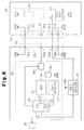
- the present embodiment may be modified as illustrated in Figure 6.
- the resistor Rc is connected between the high-potential power supply Vdd and the second terminal Tb2.
- the resistor Rh in the card information reading section 16 is connected between the second terminal Ta2 and the ground GND.
- the ADC 31 receives the voltage-divided voltage signal, obtained via the resistors Rc and Rh, as the analog signal Vi, and sends the digital signal S1 to the CPU 32. It is preferable that the first switch SW1 be connected between the second terminal Ta2 and the resistor Rh.
- the card information holding section 24 may be modified as follows.
- the card information holding section 24 shown in Figure 7A includes a plurality of diodes D connected in series between the second terminal Tb2 and the ground GND.
- the card information holding section 24 in Figure 7D includes a plurality of diodes D connected in series between the high-potential power supply Vdd and the second terminal Tb2.
- the contents of card information may be changed by changing the number of the diodes D to generate different analog voltage signals Vi.
- the analog voltage signal Vi in use is determined by the forward voltage of the diodes D times the number of the diodes D.
- the number of the diodes D is easily changed by connecting or disconnecting the diodes D.
- the CPU 32 accurately detects different analog voltage signals Vi or card information.
- the forward voltage of a silicon diode is approximately 0.6 V.
- the analog voltage signal Vi has a value of N (which is the number of the diodes D) x 0.6 V in Figure 7A and a value of Vdd - (N x 0.6 V) in Figure 7D.
- the forward voltage of a germanium diode is approximately 0.2 V.
- the analog voltage signal Vi has a value of N x 0.2 V in Figure 7A and a value of Vdd - (N x 0.2 V) in Figure 7D.
- the forward voltage of a Schottky barrier diode is about 0.3 V.
- the analog voltage signal Vi has a value of N x 0.3 V in Figure 7A and a value of Vdd - (N x 0.3 V) in Figure 7D.
- the card information holding section 24 in Figure 7B includes a plurality of Zener diodes ZD connected in series between the second terminal Tb2 and the ground GND.
- the card information holding section 24 in Figure 7E includes a plurality of Zener diodes ZD connected in series between the high-potential power supply Vdd and the second terminal Tb2.
- the analog voltage signal Vi has a value of N (which is the number of the Zener diodes ZD) x Vz (Zener voltage) in Figure 7B and a value of Vdd (N x Vz) in Figure 7E.
- the card information holding section 24 in Figure 7C includes a plurality of diodes D, a plurality of Zener diodes ZD and a resistor Rc all connected in series between the second terminal Tb2 and the ground GND.
- the card information holding section 24 in Figure 7F includes a plurality of diodes D, a plurality of Zener diodes ZD and a resistor Rc all connected in series between the high-potential power supply Vdd and the second terminal Tb2.
- the present invention may be adapted to a card-type expansion device which operates on the same operational supply voltage as the operational supply voltage Vdd of the host machine 11.
- the card main circuit 23 operates on power obtained from the high-potential supply voltage Vdd.
- the present invention may also be adapted to the host machine 11 or the card-type expansion device 21, which has a board with a pad at one edge to be connected to the associated connector.
- the card-type expansion device 21 may be connected to a host machine 11 via a drive unit (not shown). It is preferable to provide the card information reading section 16 in the drive unit.
- the drive unit reads card information from the card-type expansion device 21 and sends the read card information to the host machine 11.
- the present invention may be embodied in many other specific forms.
- the present invention may be adapted to a host machine which includes a digital camera, a digital video camera, an audio unit or the like. Therefore, the present examples and embodiments are to be considered as illustrative and not restrictive.
Landscapes
- Engineering & Computer Science (AREA)
- Power Engineering (AREA)
- Power Sources (AREA)
Applications Claiming Priority (3)
| Application Number | Priority Date | Filing Date | Title |
|---|---|---|---|
| JP28401697 | 1997-10-16 | ||
| JP284016/97 | 1997-10-16 | ||
| JP28401697A JP3364133B2 (ja) | 1997-10-16 | 1997-10-16 | カード、ホスト装置、及び、ドライブ装置 |
Publications (3)
| Publication Number | Publication Date |
|---|---|
| EP0910090A2 true EP0910090A2 (fr) | 1999-04-21 |
| EP0910090A3 EP0910090A3 (fr) | 2000-05-24 |
| EP0910090B1 EP0910090B1 (fr) | 2005-07-20 |
Family
ID=17673216
Family Applications (1)
| Application Number | Title | Priority Date | Filing Date |
|---|---|---|---|
| EP98302142A Expired - Lifetime EP0910090B1 (fr) | 1997-10-16 | 1998-03-23 | Connection d'interface pour machine hôte |
Country Status (5)
| Country | Link |
|---|---|
| US (1) | US6052742A (fr) |
| EP (1) | EP0910090B1 (fr) |
| JP (1) | JP3364133B2 (fr) |
| CN (1) | CN1106017C (fr) |
| DE (1) | DE69830881T2 (fr) |
Cited By (3)
| Publication number | Priority date | Publication date | Assignee | Title |
|---|---|---|---|---|
| EP1117026A3 (fr) * | 1999-12-29 | 2003-03-05 | Wincor Nixdorf International GmbH | Accroisement automatique de tension de fonctionnement dans des dispositifs périphériques |
| EP1158399A3 (fr) * | 2000-05-24 | 2005-08-31 | Nintendo Co., Limited | Dispositif de traitement de données et dispositif de stockage associé |
| EP1736992A1 (fr) * | 2005-06-17 | 2006-12-27 | Samsung Electronics Co., Ltd. | Dispositif et procédé de traitment de données dans un terminal sans fil avec une mémoire extern |
Families Citing this family (24)
| Publication number | Priority date | Publication date | Assignee | Title |
|---|---|---|---|---|
| US6470284B1 (en) | 1999-08-05 | 2002-10-22 | 02 Micro International Limited | Integrated PC card host controller for the detection and operation of a plurality of expansion cards |
| US6718274B2 (en) * | 1999-08-05 | 2004-04-06 | 2Micro International Limited | Integrated PC Card host controller for the detection and operation of a plurality of expansion cards |
| CN1142669C (zh) * | 2000-01-20 | 2004-03-17 | 国际商业机器公司 | 手持设备、智能卡接口设备及数据传输方法 |
| JP4378847B2 (ja) * | 2000-05-26 | 2009-12-09 | ソニー株式会社 | 電子装置を使用する機器 |
| US7269746B1 (en) * | 2000-11-27 | 2007-09-11 | Hewlett-Packard Development Company L.P. | Method of transmitting identification data from an option pack to a main unit before the option pack is fully powered |
| US6766401B2 (en) * | 2001-04-27 | 2004-07-20 | International Business Machines Corporation | Increasing control information from a single general purpose input/output (GPIO) mechanism |
| US20030051178A1 (en) * | 2001-09-12 | 2003-03-13 | Ping Liu | Mechanism for wireless modem power control |
| CN1151415C (zh) * | 2001-10-23 | 2004-05-26 | 深圳市朗科科技有限公司 | 电脑外部设备中附加存储功能的方法及其体系结构 |
| KR100433397B1 (ko) * | 2001-11-20 | 2004-06-02 | 삼성전자주식회사 | 보조전원장치 겸용 카드형장치 및 그 카드형장치를이용하는 호스트 |
| KR100440972B1 (ko) * | 2002-07-27 | 2004-07-21 | 삼성전자주식회사 | 카드 삽입 인식에 의한 데이터 전송 상태 자동 설정 장치및 방법 |
| KR100477670B1 (ko) * | 2002-09-26 | 2005-03-18 | 삼성전자주식회사 | 스마트 카드를 이용한 모니터 보안 장치 및 그 방법 |
| JP2004227239A (ja) * | 2003-01-22 | 2004-08-12 | Fujitsu Ltd | 変換装置 |
| US7073078B2 (en) * | 2003-12-12 | 2006-07-04 | Hewlett-Packard Development Company, L.P. | Power control unit that provides one of a plurality of voltages on a common power rail |
| WO2006057049A1 (fr) * | 2004-11-26 | 2006-06-01 | Kabushiki Kaisha Toshiba | Carte et dispositif hote |
| JP2008059466A (ja) * | 2006-09-01 | 2008-03-13 | Toshiba Corp | 電子機器、およびその制御方法 |
| CN201348781Y (zh) * | 2008-12-26 | 2009-11-18 | 鸿富锦精密工业(深圳)有限公司 | 电路板 |
| US8154320B1 (en) * | 2009-03-24 | 2012-04-10 | Lockheed Martin Corporation | Voltage level shifter |
| US9952791B2 (en) * | 2013-12-06 | 2018-04-24 | Samsung Electronics Co., Ltd. | Memory cards and interface circuits to communicate with memory cards |
| JP2017097825A (ja) | 2015-11-16 | 2017-06-01 | 株式会社東芝 | ホスト機器および拡張デバイス |
| JP2019046343A (ja) * | 2017-09-06 | 2019-03-22 | ブラザー工業株式会社 | 画像形成装置 |
| EP4254211A4 (fr) * | 2020-11-24 | 2024-05-01 | Panasonic Intellectual Property Management Co., Ltd. | Dispositif hôte, dispositif esclave et système de transfert de données |
| CN112816810A (zh) * | 2020-12-28 | 2021-05-18 | 国网北京市电力公司 | 数据采集装置和数据采集方法 |
| JP7722171B2 (ja) * | 2021-12-23 | 2025-08-13 | 株式会社リコー | 画像形成装置 |
| CN115421578B (zh) * | 2022-07-28 | 2025-10-17 | 飞腾信息技术有限公司 | 一种电压处理电路、方法及计算机可读存储介质 |
Family Cites Families (17)
| Publication number | Priority date | Publication date | Assignee | Title |
|---|---|---|---|---|
| JPS62232058A (ja) * | 1986-04-02 | 1987-10-12 | Meidensha Electric Mfg Co Ltd | モジユ−ルの実装枚数認識装置 |
| US5440244A (en) * | 1993-02-10 | 1995-08-08 | Cirrus Logic, Inc. | Method and apparatus for controlling a mixed voltage interface in a multivoltage system |
| JP3477781B2 (ja) * | 1993-03-23 | 2003-12-10 | セイコーエプソン株式会社 | Icカード |
| US5329491A (en) * | 1993-06-30 | 1994-07-12 | Intel Corporation | Nonvolatile memory card with automatic power supply configuration |
| US5768605A (en) * | 1994-03-16 | 1998-06-16 | Itel Corporation | Method and apparatus for power management of a PCMCIA card |
| JP3306639B2 (ja) * | 1994-04-06 | 2002-07-24 | 株式会社ワイ・イー・データ | 周辺装置 |
| US5532945A (en) * | 1994-06-17 | 1996-07-02 | Intel Corporation | Power budgetting in a computer system having removable devices |
| US5546590A (en) * | 1994-09-19 | 1996-08-13 | Intel Corporation | Power down state machine for PCMCIA PC card applications |
| US5650973A (en) * | 1994-09-27 | 1997-07-22 | Micrel, Inc. | PCMCIA power multiplexer integrated circuit with programmable decode |
| US5606704A (en) * | 1994-10-26 | 1997-02-25 | Intel Corporation | Active power down for PC card I/O applications |
| US5613130A (en) * | 1994-11-10 | 1997-03-18 | Vadem Corporation | Card voltage switching and protection |
| JPH08211973A (ja) * | 1995-01-26 | 1996-08-20 | Mitsubishi Electric Corp | Pcカード |
| US5634132A (en) * | 1995-06-23 | 1997-05-27 | Dell Usa Lp | Operating system independent support for mixed voltage devices |
| US5758171A (en) * | 1995-07-05 | 1998-05-26 | Cirrus Logic, Inc. | Apparatus and method for reading back socket power status information |
| US5805473A (en) * | 1995-08-30 | 1998-09-08 | International Business Machines Corporation | PCMCIA voltage loss detection |
| JPH1049257A (ja) * | 1996-08-05 | 1998-02-20 | Yokogawa Electric Corp | 情報処理装置 |
| US5862393A (en) * | 1996-10-07 | 1999-01-19 | Lxe, Inc. | System for managing power of a computer with removable devices |
-
1997
- 1997-10-16 JP JP28401697A patent/JP3364133B2/ja not_active Expired - Fee Related
-
1998
- 1998-03-18 US US09/040,371 patent/US6052742A/en not_active Expired - Fee Related
- 1998-03-23 EP EP98302142A patent/EP0910090B1/fr not_active Expired - Lifetime
- 1998-03-23 DE DE69830881T patent/DE69830881T2/de not_active Expired - Fee Related
- 1998-05-15 CN CN98108444.3A patent/CN1106017C/zh not_active Expired - Fee Related
Cited By (4)
| Publication number | Priority date | Publication date | Assignee | Title |
|---|---|---|---|---|
| EP1117026A3 (fr) * | 1999-12-29 | 2003-03-05 | Wincor Nixdorf International GmbH | Accroisement automatique de tension de fonctionnement dans des dispositifs périphériques |
| EP1158399A3 (fr) * | 2000-05-24 | 2005-08-31 | Nintendo Co., Limited | Dispositif de traitement de données et dispositif de stockage associé |
| EP1736992A1 (fr) * | 2005-06-17 | 2006-12-27 | Samsung Electronics Co., Ltd. | Dispositif et procédé de traitment de données dans un terminal sans fil avec une mémoire extern |
| US7552281B2 (en) | 2005-06-17 | 2009-06-23 | Samsung Electronics Co., Ltd. | Apparatus and method for processing data in a wireless terminal with external memory |
Also Published As
| Publication number | Publication date |
|---|---|
| EP0910090A3 (fr) | 2000-05-24 |
| DE69830881D1 (de) | 2005-08-25 |
| JPH11119863A (ja) | 1999-04-30 |
| US6052742A (en) | 2000-04-18 |
| EP0910090B1 (fr) | 2005-07-20 |
| CN1106017C (zh) | 2003-04-16 |
| CN1215210A (zh) | 1999-04-28 |
| JP3364133B2 (ja) | 2003-01-08 |
| DE69830881T2 (de) | 2006-04-06 |
Similar Documents
| Publication | Publication Date | Title |
|---|---|---|
| US6052742A (en) | Host machine interface for reading information stored in peripheral card prior to providing operational supply voltage to the card | |
| US6810481B1 (en) | Electronic device, control method therefor, and storage medium providing power supply control function | |
| JPS63240451A (ja) | スマート制御及びセンサデバイス付シングルワイヤバスの多重化装置 | |
| US6691201B1 (en) | Dual mode USB-PS/2 device | |
| CN108228509B (zh) | 一种usb接口切换装置和电子设备 | |
| US6832324B2 (en) | Method for providing a device communicating to a backplane the current status of an associated power supply unit connected to the backplane | |
| US6353523B1 (en) | Hot-swap protection circuitry | |
| US6883106B2 (en) | System for communicating a signal to a device indicating an output supply level being provided to a backplane from a power supply unit | |
| JP2003241730A (ja) | 表示装置 | |
| US5689430A (en) | Internal state determining apparatus | |
| US6266049B1 (en) | One-chip microcomputer system | |
| US20030056048A1 (en) | Protocol for a power supply unit controller | |
| US20120092044A1 (en) | Circuit for swapping a memory card in an electronic device | |
| CN210119772U (zh) | 复用接口设备 | |
| JPS6125593A (ja) | 洗浄機 | |
| CN114414913B (zh) | 一种工作状态的高边负载检测方法 | |
| US9013200B2 (en) | Circuitry for hot-swappable circuit boards | |
| US6822841B2 (en) | Circuit board with protection capability and method of protecting a circuit board | |
| US6154067A (en) | Methods of and apparatus for monitoring the termination status of a SCSI bus | |
| CN117240986A (zh) | 显示信号提供方法、分辨率设定装置及显示系统 | |
| KR20050069745A (ko) | 영상 표시 기기의 edid 데이터 포맷 절환 장치 | |
| CN223513642U (zh) | Hdmi接口扩展电路和显示装置 | |
| KR101139135B1 (ko) | I2c 또는 단일 와이어 브로드캐스트 인터페이스를 위한구성 가능한 데이터 포트 | |
| KR200156524Y1 (ko) | 모니터에서 온스크린디스플레이 리셋회로 | |
| CN121281403A (zh) | 一种显示屏fpc插入检测装置、方法及显示系统 |
Legal Events
| Date | Code | Title | Description |
|---|---|---|---|
| PUAI | Public reference made under article 153(3) epc to a published international application that has entered the european phase |
Free format text: ORIGINAL CODE: 0009012 |
|
| AK | Designated contracting states |
Kind code of ref document: A2 Designated state(s): DE FR GB |
|
| AX | Request for extension of the european patent |
Free format text: AL;LT;LV;MK;RO;SI |
|
| PUAL | Search report despatched |
Free format text: ORIGINAL CODE: 0009013 |
|
| AK | Designated contracting states |
Kind code of ref document: A3 Designated state(s): AT BE CH DE DK ES FI FR GB GR IE IT LI LU MC NL PT SE |
|
| AX | Request for extension of the european patent |
Free format text: AL;LT;LV;MK;RO;SI |
|
| RIC1 | Information provided on ipc code assigned before grant |
Free format text: 7G 11C 5/14 A, 7G 06K 7/00 B |
|
| 17P | Request for examination filed |
Effective date: 20001120 |
|
| AKX | Designation fees paid |
Free format text: DE FR GB |
|
| 17Q | First examination report despatched |
Effective date: 20030217 |
|
| GRAP | Despatch of communication of intention to grant a patent |
Free format text: ORIGINAL CODE: EPIDOSNIGR1 |
|
| GRAS | Grant fee paid |
Free format text: ORIGINAL CODE: EPIDOSNIGR3 |
|
| GRAA | (expected) grant |
Free format text: ORIGINAL CODE: 0009210 |
|
| AK | Designated contracting states |
Kind code of ref document: B1 Designated state(s): DE FR GB |
|
| REG | Reference to a national code |
Ref country code: GB Ref legal event code: FG4D |
|
| REF | Corresponds to: |
Ref document number: 69830881 Country of ref document: DE Date of ref document: 20050825 Kind code of ref document: P |
|
| ET | Fr: translation filed | ||
| PLBE | No opposition filed within time limit |
Free format text: ORIGINAL CODE: 0009261 |
|
| STAA | Information on the status of an ep patent application or granted ep patent |
Free format text: STATUS: NO OPPOSITION FILED WITHIN TIME LIMIT |
|
| 26N | No opposition filed |
Effective date: 20060421 |
|
| PGFP | Annual fee paid to national office [announced via postgrant information from national office to epo] |
Ref country code: GB Payment date: 20080326 Year of fee payment: 11 |
|
| PGFP | Annual fee paid to national office [announced via postgrant information from national office to epo] |
Ref country code: FR Payment date: 20080311 Year of fee payment: 11 Ref country code: DE Payment date: 20080407 Year of fee payment: 11 |
|
| GBPC | Gb: european patent ceased through non-payment of renewal fee |
Effective date: 20090323 |
|
| REG | Reference to a national code |
Ref country code: FR Ref legal event code: ST Effective date: 20091130 |
|
| PG25 | Lapsed in a contracting state [announced via postgrant information from national office to epo] |
Ref country code: DE Free format text: LAPSE BECAUSE OF NON-PAYMENT OF DUE FEES Effective date: 20091001 |
|
| PG25 | Lapsed in a contracting state [announced via postgrant information from national office to epo] |
Ref country code: GB Free format text: LAPSE BECAUSE OF NON-PAYMENT OF DUE FEES Effective date: 20090323 Ref country code: FR Free format text: LAPSE BECAUSE OF NON-PAYMENT OF DUE FEES Effective date: 20091123 |