EP0913863A2 - Procédé de fabrication d'un dispositif à semi-conducteur possédant des conducteurs en cuivre - Google Patents
Procédé de fabrication d'un dispositif à semi-conducteur possédant des conducteurs en cuivre Download PDFInfo
- Publication number
- EP0913863A2 EP0913863A2 EP98119950A EP98119950A EP0913863A2 EP 0913863 A2 EP0913863 A2 EP 0913863A2 EP 98119950 A EP98119950 A EP 98119950A EP 98119950 A EP98119950 A EP 98119950A EP 0913863 A2 EP0913863 A2 EP 0913863A2
- Authority
- EP
- European Patent Office
- Prior art keywords
- film
- copper
- copper wiring
- opening
- insulating film
- Prior art date
- Legal status (The legal status is an assumption and is not a legal conclusion. Google has not performed a legal analysis and makes no representation as to the accuracy of the status listed.)
- Withdrawn
Links
Images




Classifications
-
- H—ELECTRICITY
- H10—SEMICONDUCTOR DEVICES; ELECTRIC SOLID-STATE DEVICES NOT OTHERWISE PROVIDED FOR
- H10W—GENERIC PACKAGES, INTERCONNECTIONS, CONNECTORS OR OTHER CONSTRUCTIONAL DETAILS OF DEVICES COVERED BY CLASS H10
- H10W20/00—Interconnections in chips, wafers or substrates
- H10W20/40—Interconnections external to wafers or substrates, e.g. back-end-of-line [BEOL] metallisations or vias connecting to gate electrodes
- H10W20/41—Interconnections external to wafers or substrates, e.g. back-end-of-line [BEOL] metallisations or vias connecting to gate electrodes characterised by their conductive parts
- H10W20/425—Barrier, adhesion or liner layers
-
- H—ELECTRICITY
- H10—SEMICONDUCTOR DEVICES; ELECTRIC SOLID-STATE DEVICES NOT OTHERWISE PROVIDED FOR
- H10W—GENERIC PACKAGES, INTERCONNECTIONS, CONNECTORS OR OTHER CONSTRUCTIONAL DETAILS OF DEVICES COVERED BY CLASS H10
- H10W20/00—Interconnections in chips, wafers or substrates
- H10W20/01—Manufacture or treatment
- H10W20/031—Manufacture or treatment of conductive parts of the interconnections
- H10W20/056—Manufacture or treatment of conductive parts of the interconnections by filling conductive material into holes, grooves or trenches
-
- H—ELECTRICITY
- H10—SEMICONDUCTOR DEVICES; ELECTRIC SOLID-STATE DEVICES NOT OTHERWISE PROVIDED FOR
- H10P—GENERIC PROCESSES OR APPARATUS FOR THE MANUFACTURE OR TREATMENT OF DEVICES COVERED BY CLASS H10
- H10P50/00—Etching of wafers, substrates or parts of devices
- H10P50/20—Dry etching; Plasma etching; Reactive-ion etching
- H10P50/28—Dry etching; Plasma etching; Reactive-ion etching of insulating materials
- H10P50/282—Dry etching; Plasma etching; Reactive-ion etching of insulating materials of inorganic materials
- H10P50/283—Dry etching; Plasma etching; Reactive-ion etching of insulating materials of inorganic materials by chemical means
-
- H—ELECTRICITY
- H10—SEMICONDUCTOR DEVICES; ELECTRIC SOLID-STATE DEVICES NOT OTHERWISE PROVIDED FOR
- H10P—GENERIC PROCESSES OR APPARATUS FOR THE MANUFACTURE OR TREATMENT OF DEVICES COVERED BY CLASS H10
- H10P52/00—Grinding, lapping or polishing of wafers, substrates or parts of devices
- H10P52/40—Chemomechanical polishing [CMP]
- H10P52/403—Chemomechanical polishing [CMP] of conductive or resistive materials
-
- H—ELECTRICITY
- H10—SEMICONDUCTOR DEVICES; ELECTRIC SOLID-STATE DEVICES NOT OTHERWISE PROVIDED FOR
- H10W—GENERIC PACKAGES, INTERCONNECTIONS, CONNECTORS OR OTHER CONSTRUCTIONAL DETAILS OF DEVICES COVERED BY CLASS H10
- H10W20/00—Interconnections in chips, wafers or substrates
- H10W20/01—Manufacture or treatment
- H10W20/031—Manufacture or treatment of conductive parts of the interconnections
- H10W20/062—Manufacture or treatment of conductive parts of the interconnections by smoothing of conductive parts, e.g. by planarisation
-
- H—ELECTRICITY
- H10—SEMICONDUCTOR DEVICES; ELECTRIC SOLID-STATE DEVICES NOT OTHERWISE PROVIDED FOR
- H10W—GENERIC PACKAGES, INTERCONNECTIONS, CONNECTORS OR OTHER CONSTRUCTIONAL DETAILS OF DEVICES COVERED BY CLASS H10
- H10W20/00—Interconnections in chips, wafers or substrates
- H10W20/01—Manufacture or treatment
- H10W20/071—Manufacture or treatment of dielectric parts thereof
- H10W20/081—Manufacture or treatment of dielectric parts thereof by forming openings in the dielectric parts
-
- H—ELECTRICITY
- H10—SEMICONDUCTOR DEVICES; ELECTRIC SOLID-STATE DEVICES NOT OTHERWISE PROVIDED FOR
- H10W—GENERIC PACKAGES, INTERCONNECTIONS, CONNECTORS OR OTHER CONSTRUCTIONAL DETAILS OF DEVICES COVERED BY CLASS H10
- H10W72/00—Interconnections or connectors in packages
- H10W72/01—Manufacture or treatment
- H10W72/019—Manufacture or treatment of bond pads
-
- H—ELECTRICITY
- H10—SEMICONDUCTOR DEVICES; ELECTRIC SOLID-STATE DEVICES NOT OTHERWISE PROVIDED FOR
- H10W—GENERIC PACKAGES, INTERCONNECTIONS, CONNECTORS OR OTHER CONSTRUCTIONAL DETAILS OF DEVICES COVERED BY CLASS H10
- H10W72/00—Interconnections or connectors in packages
- H10W72/50—Bond wires
- H10W72/551—Materials of bond wires
- H10W72/552—Materials of bond wires comprising metals or metalloids, e.g. silver
- H10W72/5522—Materials of bond wires comprising metals or metalloids, e.g. silver comprising gold [Au]
-
- H—ELECTRICITY
- H10—SEMICONDUCTOR DEVICES; ELECTRIC SOLID-STATE DEVICES NOT OTHERWISE PROVIDED FOR
- H10W—GENERIC PACKAGES, INTERCONNECTIONS, CONNECTORS OR OTHER CONSTRUCTIONAL DETAILS OF DEVICES COVERED BY CLASS H10
- H10W72/00—Interconnections or connectors in packages
- H10W72/50—Bond wires
- H10W72/551—Materials of bond wires
- H10W72/552—Materials of bond wires comprising metals or metalloids, e.g. silver
- H10W72/5524—Materials of bond wires comprising metals or metalloids, e.g. silver comprising aluminium [Al]
-
- H—ELECTRICITY
- H10—SEMICONDUCTOR DEVICES; ELECTRIC SOLID-STATE DEVICES NOT OTHERWISE PROVIDED FOR
- H10W—GENERIC PACKAGES, INTERCONNECTIONS, CONNECTORS OR OTHER CONSTRUCTIONAL DETAILS OF DEVICES COVERED BY CLASS H10
- H10W72/00—Interconnections or connectors in packages
- H10W72/50—Bond wires
- H10W72/551—Materials of bond wires
- H10W72/552—Materials of bond wires comprising metals or metalloids, e.g. silver
- H10W72/5525—Materials of bond wires comprising metals or metalloids, e.g. silver comprising copper [Cu]
-
- H—ELECTRICITY
- H10—SEMICONDUCTOR DEVICES; ELECTRIC SOLID-STATE DEVICES NOT OTHERWISE PROVIDED FOR
- H10W—GENERIC PACKAGES, INTERCONNECTIONS, CONNECTORS OR OTHER CONSTRUCTIONAL DETAILS OF DEVICES COVERED BY CLASS H10
- H10W72/00—Interconnections or connectors in packages
- H10W72/50—Bond wires
- H10W72/59—Bond pads specially adapted therefor
-
- H—ELECTRICITY
- H10—SEMICONDUCTOR DEVICES; ELECTRIC SOLID-STATE DEVICES NOT OTHERWISE PROVIDED FOR
- H10W—GENERIC PACKAGES, INTERCONNECTIONS, CONNECTORS OR OTHER CONSTRUCTIONAL DETAILS OF DEVICES COVERED BY CLASS H10
- H10W72/00—Interconnections or connectors in packages
- H10W72/90—Bond pads, in general
- H10W72/921—Structures or relative sizes of bond pads
-
- H—ELECTRICITY
- H10—SEMICONDUCTOR DEVICES; ELECTRIC SOLID-STATE DEVICES NOT OTHERWISE PROVIDED FOR
- H10W—GENERIC PACKAGES, INTERCONNECTIONS, CONNECTORS OR OTHER CONSTRUCTIONAL DETAILS OF DEVICES COVERED BY CLASS H10
- H10W72/00—Interconnections or connectors in packages
- H10W72/90—Bond pads, in general
- H10W72/921—Structures or relative sizes of bond pads
- H10W72/923—Bond pads having multiple stacked layers
-
- H—ELECTRICITY
- H10—SEMICONDUCTOR DEVICES; ELECTRIC SOLID-STATE DEVICES NOT OTHERWISE PROVIDED FOR
- H10W—GENERIC PACKAGES, INTERCONNECTIONS, CONNECTORS OR OTHER CONSTRUCTIONAL DETAILS OF DEVICES COVERED BY CLASS H10
- H10W72/00—Interconnections or connectors in packages
- H10W72/90—Bond pads, in general
- H10W72/941—Dispositions of bond pads
- H10W72/9415—Dispositions of bond pads relative to the surface, e.g. recessed, protruding
-
- H—ELECTRICITY
- H10—SEMICONDUCTOR DEVICES; ELECTRIC SOLID-STATE DEVICES NOT OTHERWISE PROVIDED FOR
- H10W—GENERIC PACKAGES, INTERCONNECTIONS, CONNECTORS OR OTHER CONSTRUCTIONAL DETAILS OF DEVICES COVERED BY CLASS H10
- H10W72/00—Interconnections or connectors in packages
- H10W72/90—Bond pads, in general
- H10W72/951—Materials of bond pads
- H10W72/952—Materials of bond pads comprising metals or metalloids, e.g. PbSn, Ag or Cu
-
- H—ELECTRICITY
- H10—SEMICONDUCTOR DEVICES; ELECTRIC SOLID-STATE DEVICES NOT OTHERWISE PROVIDED FOR
- H10W—GENERIC PACKAGES, INTERCONNECTIONS, CONNECTORS OR OTHER CONSTRUCTIONAL DETAILS OF DEVICES COVERED BY CLASS H10
- H10W72/00—Interconnections or connectors in packages
- H10W72/90—Bond pads, in general
- H10W72/981—Auxiliary members, e.g. spacers
- H10W72/983—Reinforcing structures, e.g. collars
Definitions
- the present invention relates to a manufacturing method of a semiconductor device and, more particularly, to a manufacturing method of a semiconductor device using a copper wiring film.
- a copper wiring film is promised as the new wiring material after the subquarter micron generation, since copper has a low resistivity and a high electromigration resistance.
- a groove wiring method (damascene method) is used in which grooves are formed on an interlayer insulating film and wiring films are formed by using a chemical mechanical polishing (CMP) method.
- CMP chemical mechanical polishing
- the damascene method is promised as a method of realizing such copper wiring films.
- the damascene method is described in "Ultra-Low Resistance Direct Contact Cu Via Technology Using In-situ Chemical Vapor Cleaning" by Y. Tsuchiya et al., (1997 Symposium on VLSI Technology Digest of Technical Papers, pp. 59 - 60).
- FIG. 1 A case where a protective insulating film is formed and a bonding pad region is opened is shown in Fig. 1.
- reference numeral 101 denotes a Si substrate; 102 (102-1, 102-2 and 102-3) TiN films functioning as a barrier film to prevent diffusion of copper atoms and to improve fitness; 103 a copper wiring film; 104 (104-1, 104-2 and 104-3) SiO 2 films functioning as an interlayer insulating film; 105 (105-1 and 105-2) SiN films functioning as a barrier insulating film to prevent the diffusion of copper atoms; 6 a protective insulating film (it is desirable to use SiN); and 8 a copper oxide layer.
- the damascene method is a method in which after grooves are formed, the copper film 103 is deposited by a CVD (Chemical Vapor Deposition) method, a plating method, or the like. After that, the copper film 103 is polished by the CMP method with the interlayer insulating films each serving as a stopper. Thus, the excessive copper film is removed from the regions other than the wiring region. Therefore, it is difficult to form a barrier metal film on the surface of the copper wiring film. If the bonding pad portion is opened after the protective insulating films 106 is formed, the copper wiring film 103 is exposed.
- CVD Chemical Vapor Deposition
- the foregoing conventional damascene method has the following problems. That is, in particular, the copper wiring film is easily oxidized in an etching for the formation of the opening portion in the interlayer insulating film or a peeling step of a photo-resist, so that a copper oxide film 108 is formed in the bonding pad portion as shown in Fig. 1.
- a structure as shown in Fig. 2 is disclosed in Japanese Laid Open Patent Application (JP-A-Heisei 2-123740).
- TiN films 202 (202-1 and 202-2) are formed as a barrier film under the copper film and an Al film 207 is laminated on the surface of the copper wiring film 203.
- reference numeral 209 denotes a plug of material such as tungsten or the like with which a through-hole is filled.
- an object of the present invention is to provide a method of manufacturing a semiconductor device, in which a semiconductor device having good bonding performance in an assembling step is formed by using a copper wiring film by the damascene method which is excellent in the step coating performance and the flatness.
- a method of manufacturing a semiconductor device includes the steps of:
- the method may further include the step of patterning the Al containing film. Instead, the method may further include the step of performing a CMP (chemical mechanical polishing) method to the Al containing film to embed the Al containing film in the opening.
- CMP chemical mechanical polishing
- the Al containing film is selected from the group consisting of Al, Al-Si, and Al-Si-Cu.
- a whole surface of the copper wiring film other than the opening is desirably surrounded by a film for preventing copper atoms from diffusing.
- the film for preventing copper atoms from diffusing is composed of a nitride film.
- a copper oxide is removed from the copper film by a dry etching method after the formation of the opening.
- O 2 plasma etching is performed using a diluted Hf gas and a H (hfac) gas.
- the opening is an opening for an Al bonding pad.
- a method of manufacturing a semiconductor device includes the steps of:
- a method of manufacturing a semiconductor device includes the steps of:
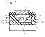
- Fig. 3 shows the cross sectional view of the structure of the semiconductor device manufactured by the method according to the first embodiment of the present invention.
- the semiconductor device is formed to have a double layer wiring film.
- a device such as MOS transistor, bipolar transistor, or the like has been formed on the Si substrate 1, it is omitted on the drawing for simplicity of explanation.
- the copper wiring film 3 is formed above the Si substrate 1 by the damascene method and a protective insulating film 6 is opened in order to form a bonding pad.
- the Al film 7 is formed on the copper wiring film 3 in the opened bonding pad portion.
- the Al film has conventionally been widely used as a metal wiring film of semiconductor device.
- the Al film has a good fitness with the bonding wire of Au, Al, or the like, and it is hard to cause the problem on the defective bonding in the assembling step.
- Figs. 4A to 4E are cross sectional views of the semiconductor device of Fig. 3 manufactured the method according to the first embodiment of the present invention in accordance with the order of manufacturing steps.
- a SiO 2 insulating film 4-1 is formed as an interlayer film by the CVD process to have the film thickness of 1 ⁇ m
- a groove having the depth of 550 nm is formed in the insulating film 4-1 by using the lithography step and dry etching step. Although its explanation is omitted here, after that, a contact hole is formed to obtain an electrode of the device.
- a TiN nitride film 2-1 is formed to have the film thickness of 50 nm, and then a copper wiring film 3 having the film thickness of 500 nm is formed by a CVD method.
- the nitride film 2-1 is formed for the purpose of prevention of the diffusion of copper and the improvement of the fitness.
- the TiN nitride film 2-1 and the copper wiring film 3 are removed from the regions other than the wiring region by a CMP (Chemical Mechanical Polishing) method.
- CMP Chemical Mechanical Polishing
- a plurality of films are formed by the CVD processes. That is, a SiN nitride film 5-1 having a film thickness of 100 nm for the prevention of diffusion of copper atoms of the copper wiring film 3, and then a SiO 2 film 4-2 is formed as an interlayer insulating film to have the film thickness of 500 nm. Subsequently, a SiN nitride 5-2 having the film thickness of 300 nm is formed for prevention of diffusion of copper atoms of the copper wiring film 3 and then a SiO 2 film 4-3 is formed as an interlayer insulating film to have the film thickness of 500 nm.
- a groove having a depth of 700 nm is formed to reach the inside of the SiN nitride film 5-2.
- a groove of 600 nm is formed as a viahole to connect to the first copper wiring film 3 which has been formed in the interlayer insulating film 4-1.
- the groove and the viahole are formed by the lithography step and dry etching step.
- the groove and the viahole are subjected to the CVD process to deposite a TiN nitride film.
- An etching-back process is performed as an anisotropic etching process to form TiN nitride films 2-2 and 2-3 having the film thickness of 50 nm on only the side walls of the groove and viahole.
- the TiN nitride films 2-2 and 2-3 prevent the diffusion of copper atoms of the copper wiring film 3 to be formed later.
- a copper oxide film is formed on the surface of the first copper wiring film 3 exposed after the etching-back process. For this reason, the copper oxide film and deposition substances formed due to the etching are removed by O 2 plasma and a diluted HF gas and a H (hfac) gas.
- a copper film is formed by a CVD process to have the film thickness of 1.3 ⁇ m. Then, the copper film is removed by a CMP process from the regions other than the wiring region. Thus, the upper portion of the copper wiring films 3 is formed by the damascene method.
- a protective insulating films (a SiN nitride film in this example) 6 is formed by a CVD process to have the film thickness of 500 nm. Then, the patterning of the protective insulating film 6 is performed by a lithography step and a dry etching step to open a bonding pad portion in the protective insulating film 6.
- a copper oxide film is formed on the surface of the upper portion of the copper wiring film 3 exposed in the etching for the opening of the bonding pad portion.
- the copper oxide film is removed by the O 2 plasma using a diluted HF gas and a H (hfac) gas.
- an Al film is deposited by a sputtering method to have the film thickness of 1 ⁇ m.
- the Al film is patterned by the lithography step and etching step to form an Al film 7 covering the bonding pad portion.
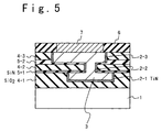
- Fig. 5 is a cross sectional diagram illustrating the structure of the semiconductor device manufactured by the method according to the second embodiment of the present invention.
- the Al film 7 is also formed by the damascene method.
- the semiconductor device manufacturing method in the second embodiment is the same as that of the first embodiment in Figs. 4A to 4D.
- the Al film is deposited by the sputtering method to have the film thickness of 1 ⁇ m.
- the Al film is subjected to the CMP process such that the Al film is left in only the bonding pad portion.
- the embedded Al film 7 is formed.
- the copper wiring film is formed by the damascene method and a protective insulating film is opened. Then, only the bonding pad portion is coated by the Al containing film.
- a copper wiring film is formed by the damascene method, and the protective insulating film is formed. Then, the bonding pad portion is formed through the protective insulating film. Thus, the copper wiring film surface is exposed.
- the Al containing film is deposited and then the CMP step or the lithography step and etching step are performed so that the Al containing film is left in only the bonding pad portion. Therefore, the problem on the fitness between the bonding wire and the bonding pad at the time of assembling is eliminated, because the Al film has good bonding performance.
- the wiring film is formed by the damascene method, the wiring having good step coating performance and flatness can be formed.
- the copper wiring film is surrounded by the copper atom diffusion preventing film formed of the nitride films such as the SiN film and the TiN film.
- the bonding pad portion of the semiconductor device on which the copper wiring film has been formed is covered by the Al film having good bonding performance, the problem about the fitness between the bonding wire and the bonding pad in the assembling step hardly occurs, so that the reliability and yield are improved.
- the copper wiring film can be formed by the damascene method, the wiring having the good step coating performance and flatness can be formed.
Landscapes
- Internal Circuitry In Semiconductor Integrated Circuit Devices (AREA)
- Wire Bonding (AREA)
Applications Claiming Priority (2)
| Application Number | Priority Date | Filing Date | Title |
|---|---|---|---|
| JP9316089A JPH11135506A (ja) | 1997-10-31 | 1997-10-31 | 半導体装置の製造方法 |
| JP316089/97 | 1997-10-31 |
Publications (2)
| Publication Number | Publication Date |
|---|---|
| EP0913863A2 true EP0913863A2 (fr) | 1999-05-06 |
| EP0913863A3 EP0913863A3 (fr) | 1999-05-19 |
Family
ID=18073129
Family Applications (1)
| Application Number | Title | Priority Date | Filing Date |
|---|---|---|---|
| EP98119950A Withdrawn EP0913863A3 (fr) | 1997-10-31 | 1998-10-21 | Procédé de fabrication d'un dispositif à semi-conducteur possédant des conducteurs en cuivre |
Country Status (5)
| Country | Link |
|---|---|
| EP (1) | EP0913863A3 (fr) |
| JP (1) | JPH11135506A (fr) |
| KR (1) | KR19990037442A (fr) |
| CN (1) | CN1216398A (fr) |
| TW (1) | TW423076B (fr) |
Cited By (13)
| Publication number | Priority date | Publication date | Assignee | Title |
|---|---|---|---|---|
| WO1999030363A3 (fr) * | 1997-12-10 | 1999-08-26 | Koninkl Philips Electronics Nv | Dispositif a semiconducteur et procede de fabrication de ce dernier |
| WO2000077853A1 (fr) * | 1999-06-10 | 2000-12-21 | Infineon Technologies Ag | CONFIGURATION DE FUSIBLES DANS DES STRUCTURES A SEMI-CONDUCTEUR A METALLISATION Cu |
| FR2798512A1 (fr) * | 1999-09-14 | 2001-03-16 | Commissariat Energie Atomique | Procede de realisation d'une connexion en cuivre au travers d'une couche de materiau dielectrique d'un circuit integre |
| US6399477B2 (en) | 2000-02-03 | 2002-06-04 | Seiko Epson Corporation | Semiconductor devices and methods for manufacturing semiconductor devices |
| EP1119046A3 (fr) * | 2000-01-21 | 2002-07-03 | Lucent Technologies Inc. | Technique pour connexion de fils et architecture pour la métallisation en cuivre pour structures semi-conductrices |
| US6498090B2 (en) | 2000-02-03 | 2002-12-24 | Seiko Epson Corporation | Semiconductor devices and methods for manufacturing the same |
| US6727590B2 (en) | 2001-11-01 | 2004-04-27 | Renesas Technology Corp. | Semiconductor device with internal bonding pad |
| DE10059773B4 (de) * | 2000-06-07 | 2004-04-29 | Mitsubishi Denki K.K. | Halbleitervorrichtung |
| US7279790B2 (en) | 2001-08-29 | 2007-10-09 | Fujitsu Limited | Semiconductor device and a manufacturing method thereof |
| US7485962B2 (en) | 2002-12-10 | 2009-02-03 | Fujitsu Limited | Semiconductor device, wiring substrate forming method, and substrate processing apparatus |
| EP2290686A3 (fr) * | 2009-08-28 | 2011-04-20 | STMicroelectronics S.r.l. | Procédé pour effectuer le test électrique et l'assemblage de dispositifs électroniques |
| US8378346B2 (en) | 2008-08-07 | 2013-02-19 | Stmicroelectronics S.R.L. | Circuit architecture for the parallel supplying during electric or electromagnetic testing of a plurality of electronic devices integrated on a semiconductor wafer |
| EP3301711A3 (fr) * | 2016-09-30 | 2018-06-06 | Semiconductor Manufacturing International Corporation (Beijing) | Procédé pour améliorer la résistance de soudure de fils d'un capteur d'images |
Families Citing this family (18)
| Publication number | Priority date | Publication date | Assignee | Title |
|---|---|---|---|---|
| KR100333712B1 (ko) * | 1999-06-24 | 2002-04-24 | 박종섭 | 반도체 소자의 상감형 금속배선 형성방법 |
| GB2364170B (en) * | 1999-12-16 | 2002-06-12 | Lucent Technologies Inc | Dual damascene bond pad structure for lowering stress and allowing circuitry under pads and a process to form the same |
| JP3602024B2 (ja) * | 2000-01-21 | 2004-12-15 | シャープ株式会社 | 半導体装置及びその製造方法 |
| KR100370238B1 (ko) * | 2000-10-20 | 2003-01-30 | 삼성전자 주식회사 | 반도체 소자의 본드패드 및 그 형성방법 |
| US6693343B2 (en) * | 2000-12-28 | 2004-02-17 | Infineon Technologies Ag | Self-passivating Cu laser fuse |
| US6727593B2 (en) | 2001-03-01 | 2004-04-27 | Kabushiki Kaisha Toshiba | Semiconductor device with improved bonding |
| JP2002329722A (ja) | 2001-04-27 | 2002-11-15 | Nec Corp | 半導体装置及びその製造方法 |
| JP2003031575A (ja) * | 2001-07-17 | 2003-01-31 | Nec Corp | 半導体装置及びその製造方法 |
| JP2003142579A (ja) * | 2001-11-07 | 2003-05-16 | Hitachi Ltd | 半導体装置の製造方法および半導体装置 |
| CN100547741C (zh) * | 2002-12-10 | 2009-10-07 | 富士通株式会社 | 半导体装置、布线衬底的形成方法和衬底处理装置 |
| JP2004221098A (ja) | 2003-01-09 | 2004-08-05 | Renesas Technology Corp | 半導体装置およびその製造方法 |
| JP4170103B2 (ja) * | 2003-01-30 | 2008-10-22 | Necエレクトロニクス株式会社 | 半導体装置、および半導体装置の製造方法 |
| JP2007042662A (ja) * | 2003-10-20 | 2007-02-15 | Renesas Technology Corp | 半導体装置 |
| JP2008091454A (ja) * | 2006-09-29 | 2008-04-17 | Rohm Co Ltd | 半導体装置及び半導体装置の製造方法 |
| JP2008135692A (ja) * | 2006-10-24 | 2008-06-12 | Denso Corp | 半導体装置 |
| US7741218B2 (en) * | 2007-02-27 | 2010-06-22 | Freescale Semiconductor, Inc. | Conductive via formation utilizing electroplating |
| JP5805708B2 (ja) * | 2013-06-05 | 2015-11-04 | 株式会社神戸製鋼所 | タッチパネルセンサー用配線膜、およびタッチパネルセンサー |
| JP7319075B2 (ja) * | 2019-03-29 | 2023-08-01 | ローム株式会社 | 半導体装置および半導体パッケージ |
Family Cites Families (8)
| Publication number | Priority date | Publication date | Assignee | Title |
|---|---|---|---|---|
| JPS6376455A (ja) * | 1986-09-19 | 1988-04-06 | Fujitsu Ltd | 半導体装置の製造方法 |
| JPH02123740A (ja) * | 1988-11-02 | 1990-05-11 | Mitsubishi Electric Corp | 半導体装置 |
| JP3072807B2 (ja) * | 1992-07-15 | 2000-08-07 | 日本電信電話株式会社 | 半導体装置の製造方法 |
| JP3326698B2 (ja) * | 1993-03-19 | 2002-09-24 | 富士通株式会社 | 集積回路装置の製造方法 |
| JP2560625B2 (ja) * | 1993-10-29 | 1996-12-04 | 日本電気株式会社 | 半導体装置およびその製造方法 |
| JPH0878410A (ja) * | 1994-09-05 | 1996-03-22 | Mitsubishi Electric Corp | 配線接続部及びその製造方法 |
| EP0751566A3 (fr) * | 1995-06-30 | 1997-02-26 | Ibm | Couche de barrière comprenant un film métallique mince pour des interconnexions électriques |
| US5785236A (en) * | 1995-11-29 | 1998-07-28 | Advanced Micro Devices, Inc. | Advanced copper interconnect system that is compatible with existing IC wire bonding technology |
-
1997
- 1997-10-31 JP JP9316089A patent/JPH11135506A/ja active Pending
-
1998
- 1998-10-08 TW TW087116767A patent/TW423076B/zh not_active IP Right Cessation
- 1998-10-21 EP EP98119950A patent/EP0913863A3/fr not_active Withdrawn
- 1998-10-26 CN CN98120479A patent/CN1216398A/zh active Pending
- 1998-10-28 KR KR1019980045358A patent/KR19990037442A/ko not_active Ceased
Cited By (24)
| Publication number | Priority date | Publication date | Assignee | Title |
|---|---|---|---|---|
| WO1999030363A3 (fr) * | 1997-12-10 | 1999-08-26 | Koninkl Philips Electronics Nv | Dispositif a semiconducteur et procede de fabrication de ce dernier |
| US6201291B1 (en) | 1997-12-10 | 2001-03-13 | U.S. Philips Corporation | Semiconductor device and method of manufacturing such a device |
| WO2000077853A1 (fr) * | 1999-06-10 | 2000-12-21 | Infineon Technologies Ag | CONFIGURATION DE FUSIBLES DANS DES STRUCTURES A SEMI-CONDUCTEUR A METALLISATION Cu |
| US6774456B2 (en) | 1999-06-10 | 2004-08-10 | Infineon Technologies Ag | Configuration of fuses in semiconductor structures with Cu metallization |
| FR2798512A1 (fr) * | 1999-09-14 | 2001-03-16 | Commissariat Energie Atomique | Procede de realisation d'une connexion en cuivre au travers d'une couche de materiau dielectrique d'un circuit integre |
| WO2001020665A1 (fr) * | 1999-09-14 | 2001-03-22 | Commissariat A L'energie Atomique | Procede de realisation d'une connexion en cuivre |
| US6521533B1 (en) | 1999-09-14 | 2003-02-18 | Commissariat A L'energie Atomique | Method for producing a copper connection |
| EP1119046A3 (fr) * | 2000-01-21 | 2002-07-03 | Lucent Technologies Inc. | Technique pour connexion de fils et architecture pour la métallisation en cuivre pour structures semi-conductrices |
| US6399477B2 (en) | 2000-02-03 | 2002-06-04 | Seiko Epson Corporation | Semiconductor devices and methods for manufacturing semiconductor devices |
| US6498090B2 (en) | 2000-02-03 | 2002-12-24 | Seiko Epson Corporation | Semiconductor devices and methods for manufacturing the same |
| US6559545B2 (en) * | 2000-02-03 | 2003-05-06 | Seiko Epson Corporation | Semiconductor devices and methods for manufacturing semiconductor devices |
| US6710460B2 (en) | 2000-02-03 | 2004-03-23 | Seiko Epson Corporation | Semiconductor devices and methods for manufacturing the same |
| DE10059773B4 (de) * | 2000-06-07 | 2004-04-29 | Mitsubishi Denki K.K. | Halbleitervorrichtung |
| US7279790B2 (en) | 2001-08-29 | 2007-10-09 | Fujitsu Limited | Semiconductor device and a manufacturing method thereof |
| US6727590B2 (en) | 2001-11-01 | 2004-04-27 | Renesas Technology Corp. | Semiconductor device with internal bonding pad |
| US7485962B2 (en) | 2002-12-10 | 2009-02-03 | Fujitsu Limited | Semiconductor device, wiring substrate forming method, and substrate processing apparatus |
| US7648907B2 (en) | 2002-12-10 | 2010-01-19 | Fujitsu Limited | Semiconductor device, wiring substrate forming method, and substrate processing apparatus |
| US7704856B2 (en) | 2002-12-10 | 2010-04-27 | Fujitsu Limited | Semiconductor device, wiring substrate forming method, and substrate processing apparatus |
| US8378346B2 (en) | 2008-08-07 | 2013-02-19 | Stmicroelectronics S.R.L. | Circuit architecture for the parallel supplying during electric or electromagnetic testing of a plurality of electronic devices integrated on a semiconductor wafer |
| EP2290686A3 (fr) * | 2009-08-28 | 2011-04-20 | STMicroelectronics S.r.l. | Procédé pour effectuer le test électrique et l'assemblage de dispositifs électroniques |
| US8362620B2 (en) | 2009-08-28 | 2013-01-29 | Stmicroelectronics S.R.L. | Electronic devices with extended metallization layer on a passivation layer |
| US8941108B2 (en) | 2009-08-28 | 2015-01-27 | Stmicroelectronics S.R.L. | Method to perform electrical testing and assembly of electronic devices |
| EP3301711A3 (fr) * | 2016-09-30 | 2018-06-06 | Semiconductor Manufacturing International Corporation (Beijing) | Procédé pour améliorer la résistance de soudure de fils d'un capteur d'images |
| US11133275B2 (en) | 2016-09-30 | 2021-09-28 | Semiconductor Manufacturing International (Beijing) Corporation | Method for improving wire bonding strength of an image sensor |
Also Published As
| Publication number | Publication date |
|---|---|
| KR19990037442A (ko) | 1999-05-25 |
| JPH11135506A (ja) | 1999-05-21 |
| CN1216398A (zh) | 1999-05-12 |
| EP0913863A3 (fr) | 1999-05-19 |
| TW423076B (en) | 2001-02-21 |
Similar Documents
| Publication | Publication Date | Title |
|---|---|---|
| EP0913863A2 (fr) | Procédé de fabrication d'un dispositif à semi-conducteur possédant des conducteurs en cuivre | |
| US6294835B1 (en) | Self-aligned composite insulator with sub-half-micron multilevel high density electrical interconnections and process thereof | |
| US6143672A (en) | Method of reducing metal voidings in 0.25 μm AL interconnect | |
| US6355555B1 (en) | Method of fabricating copper-based semiconductor devices using a sacrificial dielectric layer | |
| US6261963B1 (en) | Reverse electroplating of barrier metal layer to improve electromigration performance in copper interconnect devices | |
| US7154182B2 (en) | Localized slots for stress relieve in copper | |
| CN100499067C (zh) | 适用于形成互连的方法和装置 | |
| KR20030035909A (ko) | 반도체장치 및 그 제조방법 | |
| JP2004064046A (ja) | 半導体装置及びその製造方法 | |
| JP2002329722A (ja) | 半導体装置及びその製造方法 | |
| US6169028B1 (en) | Method fabricating metal interconnected structure | |
| US4920403A (en) | Selective tungsten interconnection for yield enhancement | |
| US20010001742A1 (en) | Method of fabricating a dual -damascene structure in an integrated cirtcuit with multilevel-interconnect strcture | |
| JP3012187B2 (ja) | 半導体装置の製造方法 | |
| US6033984A (en) | Dual damascene with bond pads | |
| JPH11186391A (ja) | 半導体装置およびその製造方法 | |
| US6313037B1 (en) | Semiconductor device and method for manufacturing the same | |
| JP3063338B2 (ja) | 半導体装置およびその製造方法 | |
| US6180506B1 (en) | Upper redundant layer for damascene metallization | |
| US20020061644A1 (en) | Method of manufacturing an amorphized barrier layer for integrated circuit interconnects | |
| US20020106895A1 (en) | Method for forming copper interconnect and enhancing electromigration resistance | |
| US6200890B1 (en) | Method of fabricating copper damascene | |
| US20020127849A1 (en) | Method of manufacturing dual damascene structure | |
| US6479898B1 (en) | Dielectric treatment in integrated circuit interconnects | |
| US6509257B1 (en) | Semiconductor device and process for making the same |
Legal Events
| Date | Code | Title | Description |
|---|---|---|---|
| PUAI | Public reference made under article 153(3) epc to a published international application that has entered the european phase |
Free format text: ORIGINAL CODE: 0009012 |
|
| PUAL | Search report despatched |
Free format text: ORIGINAL CODE: 0009013 |
|
| AK | Designated contracting states |
Kind code of ref document: A2 Designated state(s): DE FR GB |
|
| AX | Request for extension of the european patent |
Free format text: AL;LT;LV;MK;RO;SI |
|
| AK | Designated contracting states |
Kind code of ref document: A3 Designated state(s): AT BE CH CY DE DK ES FI FR GB GR IE IT LI LU MC NL PT SE |
|
| AX | Request for extension of the european patent |
Free format text: AL;LT;LV;MK;RO;SI |
|
| 17P | Request for examination filed |
Effective date: 19990408 |
|
| AKX | Designation fees paid |
Free format text: DE FR GB |
|
| 17Q | First examination report despatched |
Effective date: 20020129 |
|
| STAA | Information on the status of an ep patent application or granted ep patent |
Free format text: STATUS: THE APPLICATION IS DEEMED TO BE WITHDRAWN |
|
| 18D | Application deemed to be withdrawn |
Effective date: 20020611 |