EP0914028A2 - Zwischenstück - Google Patents
Zwischenstück Download PDFInfo
- Publication number
- EP0914028A2 EP0914028A2 EP98308773A EP98308773A EP0914028A2 EP 0914028 A2 EP0914028 A2 EP 0914028A2 EP 98308773 A EP98308773 A EP 98308773A EP 98308773 A EP98308773 A EP 98308773A EP 0914028 A2 EP0914028 A2 EP 0914028A2
- Authority
- EP
- European Patent Office
- Prior art keywords
- contact
- spring
- projection
- noses
- assembly according
- Prior art date
- Legal status (The legal status is an assumption and is not a legal conclusion. Google has not performed a legal analysis and makes no representation as to the accuracy of the status listed.)
- Granted
Links
- 210000001331 nose Anatomy 0.000 claims abstract description 19
- 230000014759 maintenance of location Effects 0.000 claims abstract description 17
- 229910052751 metal Inorganic materials 0.000 claims abstract description 5
- 239000002184 metal Substances 0.000 claims abstract description 5
- 238000003780 insertion Methods 0.000 abstract description 3
- 230000037431 insertion Effects 0.000 abstract description 3
- 230000000295 complement effect Effects 0.000 abstract 1
- 230000000712 assembly Effects 0.000 description 10
- 238000000429 assembly Methods 0.000 description 10
- 239000000919 ceramic Substances 0.000 description 5
- 238000005452 bending Methods 0.000 description 2
- 238000003491 array Methods 0.000 description 1
- DMFGNRRURHSENX-UHFFFAOYSA-N beryllium copper Chemical compound [Be].[Cu] DMFGNRRURHSENX-UHFFFAOYSA-N 0.000 description 1
- 210000000887 face Anatomy 0.000 description 1
- 230000005484 gravity Effects 0.000 description 1
- 238000009434 installation Methods 0.000 description 1
- 239000011810 insulating material Substances 0.000 description 1
- 238000004519 manufacturing process Methods 0.000 description 1
- 230000000284 resting effect Effects 0.000 description 1
- 239000000758 substrate Substances 0.000 description 1
Images

Classifications
-
- H—ELECTRICITY
- H01—ELECTRIC ELEMENTS
- H01R—ELECTRICALLY-CONDUCTIVE CONNECTIONS; STRUCTURAL ASSOCIATIONS OF A PLURALITY OF MUTUALLY-INSULATED ELECTRICAL CONNECTING ELEMENTS; COUPLING DEVICES; CURRENT COLLECTORS
- H01R13/00—Details of coupling devices of the kinds covered by groups H01R12/70 or H01R24/00 - H01R33/00
- H01R13/02—Contact members
- H01R13/22—Contacts for co-operating by abutting
- H01R13/24—Contacts for co-operating by abutting resilient; resiliently-mounted
- H01R13/2435—Contacts for co-operating by abutting resilient; resiliently-mounted with opposite contact points, e.g. C beam
-
- H—ELECTRICITY
- H01—ELECTRIC ELEMENTS
- H01R—ELECTRICALLY-CONDUCTIVE CONNECTIONS; STRUCTURAL ASSOCIATIONS OF A PLURALITY OF MUTUALLY-INSULATED ELECTRICAL CONNECTING ELEMENTS; COUPLING DEVICES; CURRENT COLLECTORS
- H01R12/00—Structural associations of a plurality of mutually-insulated electrical connecting elements, specially adapted for printed circuits, e.g. printed circuit boards [PCB], flat or ribbon cables, or like generally planar structures, e.g. terminal strips, terminal blocks; Coupling devices specially adapted for printed circuits, flat or ribbon cables, or like generally planar structures; Terminals specially adapted for contact with, or insertion into, printed circuits, flat or ribbon cables, or like generally planar structures
- H01R12/70—Coupling devices
- H01R12/7082—Coupling device supported only by cooperation with PCB
-
- H—ELECTRICITY
- H05—ELECTRIC TECHNIQUES NOT OTHERWISE PROVIDED FOR
- H05K—PRINTED CIRCUITS; CASINGS OR CONSTRUCTIONAL DETAILS OF ELECTRIC APPARATUS; MANUFACTURE OF ASSEMBLAGES OF ELECTRICAL COMPONENTS
- H05K7/00—Constructional details common to different types of electric apparatus
- H05K7/02—Arrangements of circuit components or wiring on supporting structure
- H05K7/10—Plug-in assemblages of components, e.g. IC sockets
- H05K7/1053—Plug-in assemblages of components, e.g. IC sockets having interior leads
- H05K7/1061—Plug-in assemblages of components, e.g. IC sockets having interior leads co-operating by abutting
- H05K7/1069—Plug-in assemblages of components, e.g. IC sockets having interior leads co-operating by abutting with spring contact pieces
-
- H—ELECTRICITY
- H01—ELECTRIC ELEMENTS
- H01R—ELECTRICALLY-CONDUCTIVE CONNECTIONS; STRUCTURAL ASSOCIATIONS OF A PLURALITY OF MUTUALLY-INSULATED ELECTRICAL CONNECTING ELEMENTS; COUPLING DEVICES; CURRENT COLLECTORS
- H01R12/00—Structural associations of a plurality of mutually-insulated electrical connecting elements, specially adapted for printed circuits, e.g. printed circuit boards [PCB], flat or ribbon cables, or like generally planar structures, e.g. terminal strips, terminal blocks; Coupling devices specially adapted for printed circuits, flat or ribbon cables, or like generally planar structures; Terminals specially adapted for contact with, or insertion into, printed circuits, flat or ribbon cables, or like generally planar structures
- H01R12/70—Coupling devices
- H01R12/71—Coupling devices for rigid printing circuits or like structures
- H01R12/712—Coupling devices for rigid printing circuits or like structures co-operating with the surface of the printed circuit or with a coupling device exclusively provided on the surface of the printed circuit
- H01R12/714—Coupling devices for rigid printing circuits or like structures co-operating with the surface of the printed circuit or with a coupling device exclusively provided on the surface of the printed circuit with contacts abutting directly the printed circuit; Button contacts therefore provided on the printed circuit
Definitions
- the invention relates to interposer assemblies used for forming electrical connections between contact pads on circuit members.
- Interposer assemblies are used for forming electrical connections between densely spaced contact pads on adjacentparallel circuit members.
- the pads on the members are arranged in identical patterns.
- the circuit members are a circuit board and a ceramic plate carrying integrated circuits.
- the interposer assembly includes an insulating plate and a plurality of through-contacts carried in the plate and arranged in the same pattern as the pads on the circuit members.
- the contacts project above the top and bottom of the plate.
- the assembly is sandwiched between the two members which are held together with the contacts forming electric connections between appropriate aligned pairs of pads.
- Interposer assemblies are used for forming electricalconnections between contact pads arranged in a very close proximity to each other.
- the pads may be arranged on a one millimeter center-to-center grid.
- the contacts In addition to requiringcontacts which can be spaced very close to each other, the contacts must form reliable electrical connections with the pads when the assemblies are sandwiched between the circuit members.
- a low mechanical closure force is required in order to prevent undue stress to a ceramic circuit member.
- a high closure force could distort or possibly break the ceramic member.
- interposer assemblies must occupy a minimum width space between the circuit members, requiring that the individual electrical contacts in the assembly have a limited height yet possess the required spring properties for establishing reliable electrical connections between the pads without undue closing force.
- the invention is an improved interposer assembly including metal contacts loosely confined in closely spaced passages extending through an insulating plate.
- the contacts include arcuate spring portions which are elastically bent to form wiped connections with the pads and reduce the force necessary to sandwich the interposer assembly between the circuit members.
- the low closure force reduces the risk of damage to an overlying ceramic substrate and allows a large number of contacts in the assembly.
- the wiped electrical connections between the contacts and the circuit pads form reliable electrical connections between the adjacent pairs of pads and permit installation of the interposer assemblies in user's facilities. The assemblies need not be installed in clean rooms.
- the disclosed interposer assembly uses plates and contacts which are easily and inexpensively manufactured and assembled.
- the plate is a one-piece design and includes through passages with contact retention projections extending into the passages.
- the contacts are generally D-shaped and are readily inserted into the passages to snap or latch over the projections, which then hold the contacts loosely in place in the passages prior to sandwiching of the assemblies between circuit members.
- the contacts are compact, permitting use of the assembly to form electrical connections between very closely spaced contact pads.
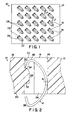
- Interposer assembly 10 includes a flat plate 12 formed of insulating material with a plurality of metal contacts 14 positioned in passages 16 extending through the thickness of the plate between opposed plate top and bottom surfaces 18 and 20. As shown in Figure 1, passages 16 are each provided with a reduced width side 22 and a uniform width portion 24 away from side 22. Flat side wall 26 extends across the uniform width portions 24 opposite the reduced width side 22.
- Contact retention projections are provided in the reduced width sides 22 of passages 16.
- Projections 28 extend a distance into the passages and include contact retention surfaces 30 and 32 facing plate top and bottom 18 and 20, respectively.
- the surfaces 30 and 32 are spaced in from the top and bottom of the plate.
- a sloped cam surface 34 extends from each retention surface 30 to the inner end of the projection 28 and faces upwardly. Surface 34 facilitates insertion of contact 14 into passage 16.
- Each metal contact 14 is preferably formed from uniformthickness strip stock, which may be suitably plated beryllium copper.
- the contact is generally D-shaped and includes a arcuate, convex spring 36 with a pair of opposed contact noses 38 at the ends of the springs. The noses are spaced apart a distance greater than the thickness of the plate 12.
- Short retention legs 40 extend inwardly from the noses to free ends 42. The legs 40 extend away from spring 36 so that the noses 38 are located between the free ends 42 and the spring.
- spring 36 has a maximum width midway between noses 36 and includes two tapered width spring portions or arms 44 each extending from the center of the spring to a nose 38, in order to reduce stress concentration when the spring is stressed.
- Contacts 14 are inserted into passages 16 as shown in Figure 6.
- One nose of the contact is extended into the end of the passage opening at plate top 18 and is positioned between the projection 28 and end wall 26.
- the contact is inserted into the passage and leg 40 is guided by surface 34 to the end of the projection and spring 36 engages wall 26.
- the contact is then inserted further into the passage with the result that the lower spring arm 44 is elastically stressed, leg 40 is moved past projection 28 and snaps back under retention surface 32.
- end 42 of the upper retention leg 40 is above the upper retention surface 30, end 42 of the lower retention leg 40 is located below the lower retention surface 32 and the center 41 of the arcuate spring is adjacent the flat end wall 26.
- Spring 36 is bowed toward wall 26.
- FIG. 1 illustrates the position of the contact in the passage when plate 12 is horizontal and the loose contact 14 is supported in the cavity against gravity with the end of the upper leg 40 resting on upper retention surface 30 of projection 28.
- the passages 16 are arranged close to each other in a dense array on plate 12 in order to permit forming of electrical connections between similar arrays of contact pads on circuit elements located above and below the assembly.
- assembly 10 is used for forming electrical connections between contact pads on a ceramic integrated circuit and contact pads of a circuit board.
- the assembly may be used for forming electrical connections between contact pads on two circuit boards or between contact pads on other types of circuit members.
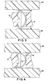
- Figure 3 illustrates the interposer assembly 10 positioned between upper and lower circuit members 46 and 48 with contact, pads 50 and 52 on the members located above and below each contact in the assembly. The contacts lightly engage the pads and are not stressed.
- Figure 4 illustrates the assembly 10 when fully sandwiched between member 46 and 48 with the members held tightly against the assembly plate 12.
- the two contact pads 50 and 52 are moved together to reduce the height of contacts 14 and elastically bend the two tapered spring arms 44 of arcuate spring 36.
- the center of the spring engages the side wall 26 as shown in Figure 4. Bending of the arcuate spring and foreshortening of the contact moves or wipes the contact noses 38 a distance along the contact pads toward side 22 to make clean, low resistance pressure electrical connections between the contact noses 38 and the pads 50 and 52.
- the connections assure that the contact 14 provides a reliable, low resistance electrical path between the pads.
Landscapes
- Engineering & Computer Science (AREA)
- Microelectronics & Electronic Packaging (AREA)
- Coupling Device And Connection With Printed Circuit (AREA)
Priority Applications (1)
| Application Number | Priority Date | Filing Date | Title |
|---|---|---|---|
| EP01104395A EP1111977B1 (fr) | 1997-10-30 | 1998-10-27 | Pièce d'interposition |
Applications Claiming Priority (2)
| Application Number | Priority Date | Filing Date | Title |
|---|---|---|---|
| US96095397A | 1997-10-30 | 1997-10-30 | |
| US960953 | 1997-10-30 |
Related Child Applications (1)
| Application Number | Title | Priority Date | Filing Date |
|---|---|---|---|
| EP01104395A Division EP1111977B1 (fr) | 1997-10-30 | 1998-10-27 | Pièce d'interposition |
Publications (3)
| Publication Number | Publication Date |
|---|---|
| EP0914028A2 true EP0914028A2 (fr) | 1999-05-06 |
| EP0914028A3 EP0914028A3 (fr) | 2000-03-15 |
| EP0914028B1 EP0914028B1 (fr) | 2005-02-09 |
Family
ID=25503869
Family Applications (2)
| Application Number | Title | Priority Date | Filing Date |
|---|---|---|---|
| EP01104395A Expired - Lifetime EP1111977B1 (fr) | 1997-10-30 | 1998-10-27 | Pièce d'interposition |
| EP19980308773 Expired - Lifetime EP0914028B1 (fr) | 1997-10-30 | 1998-10-27 | Zwischenstück |
Family Applications Before (1)
| Application Number | Title | Priority Date | Filing Date |
|---|---|---|---|
| EP01104395A Expired - Lifetime EP1111977B1 (fr) | 1997-10-30 | 1998-10-27 | Pièce d'interposition |
Country Status (4)
| Country | Link |
|---|---|
| EP (2) | EP1111977B1 (fr) |
| JP (1) | JP2967087B2 (fr) |
| CA (1) | CA2249885C (fr) |
| DE (2) | DE69828937T2 (fr) |
Cited By (5)
| Publication number | Priority date | Publication date | Assignee | Title |
|---|---|---|---|---|
| US6921270B2 (en) | 2003-06-11 | 2005-07-26 | Cinch Connectors, Inc. | Electrical connector |
| US7455556B2 (en) | 2003-06-11 | 2008-11-25 | Cinch Connectors, Inc. | Electrical contact |
| US7625216B2 (en) | 2003-06-11 | 2009-12-01 | Cinch Connectors, Inc. | Electrical connector |
| CN112290334A (zh) * | 2019-07-23 | 2021-01-29 | 泰科电子日本合同会社 | 内插器 |
| CN113540855A (zh) * | 2020-04-22 | 2021-10-22 | 泰科电子(上海)有限公司 | 弹性端子、弹性端子的制作方法、电连接器和电子设备 |
Families Citing this family (2)
| Publication number | Priority date | Publication date | Assignee | Title |
|---|---|---|---|---|
| US9583426B2 (en) * | 2014-11-05 | 2017-02-28 | Invensas Corporation | Multi-layer substrates suitable for interconnection between circuit modules |
| CN117353064A (zh) * | 2022-06-28 | 2024-01-05 | 中兴智能科技南京有限公司 | 端子、连接器及电子设备 |
Family Cites Families (8)
| Publication number | Priority date | Publication date | Assignee | Title |
|---|---|---|---|---|
| US4513353A (en) | 1982-12-27 | 1985-04-23 | Amp Incorporated | Connection of leadless integrated circuit package to a circuit board |
| US4647124A (en) | 1985-10-16 | 1987-03-03 | Amp Incorporated | Electrical connector for interconnecting arrays of conductive areas |
| US4699593A (en) | 1986-01-14 | 1987-10-13 | Amp Incorporated | Connector having contact modules for a substrate such as an IC chip carrier |
| US4906194A (en) | 1989-04-13 | 1990-03-06 | Amp Incorporated | High density connector for an IC chip carrier |
| FR2655484B1 (fr) * | 1989-12-06 | 1995-06-09 | Amp Inc | Ensemble connecteur pour puces a circuits integres et modules de contact pour cet ensemble. |
| JPH0713191Y2 (ja) * | 1991-02-20 | 1995-03-29 | 日本航空電子工業株式会社 | コネクタ |
| EP0742682B1 (fr) * | 1995-05-12 | 2005-02-23 | STMicroelectronics, Inc. | Système de conditionnement pour circuit intégré par socle à profil bas |
| US5653598A (en) * | 1995-08-31 | 1997-08-05 | The Whitaker Corporation | Electrical contact with reduced self-inductance |
-
1998
- 1998-10-08 CA CA002249885A patent/CA2249885C/fr not_active Expired - Fee Related
- 1998-10-27 EP EP01104395A patent/EP1111977B1/fr not_active Expired - Lifetime
- 1998-10-27 DE DE1998628937 patent/DE69828937T2/de not_active Expired - Lifetime
- 1998-10-27 DE DE1998630081 patent/DE69830081T2/de not_active Expired - Lifetime
- 1998-10-27 EP EP19980308773 patent/EP0914028B1/fr not_active Expired - Lifetime
- 1998-10-29 JP JP10308243A patent/JP2967087B2/ja not_active Expired - Lifetime
Cited By (10)
| Publication number | Priority date | Publication date | Assignee | Title |
|---|---|---|---|---|
| US6921270B2 (en) | 2003-06-11 | 2005-07-26 | Cinch Connectors, Inc. | Electrical connector |
| US7094066B2 (en) | 2003-06-11 | 2006-08-22 | Cinch Connectors, Inc. | Electrical connector |
| US7261567B2 (en) | 2003-06-11 | 2007-08-28 | Cinch Connectors, Inc. | Electrical connector |
| US7263770B2 (en) | 2003-06-11 | 2007-09-04 | Cinch Connectors, Inc. | Electrical connector |
| US7455556B2 (en) | 2003-06-11 | 2008-11-25 | Cinch Connectors, Inc. | Electrical contact |
| US7614883B2 (en) | 2003-06-11 | 2009-11-10 | Cinch Connectors, Inc. | Electrical connector |
| US7625216B2 (en) | 2003-06-11 | 2009-12-01 | Cinch Connectors, Inc. | Electrical connector |
| CN112290334A (zh) * | 2019-07-23 | 2021-01-29 | 泰科电子日本合同会社 | 内插器 |
| CN112290334B (zh) * | 2019-07-23 | 2024-03-08 | 泰科电子日本合同会社 | 内插器 |
| CN113540855A (zh) * | 2020-04-22 | 2021-10-22 | 泰科电子(上海)有限公司 | 弹性端子、弹性端子的制作方法、电连接器和电子设备 |
Also Published As
| Publication number | Publication date |
|---|---|
| JP2967087B2 (ja) | 1999-10-25 |
| JPH11204215A (ja) | 1999-07-30 |
| DE69830081T2 (de) | 2005-09-22 |
| DE69828937T2 (de) | 2005-07-07 |
| DE69830081D1 (de) | 2005-06-09 |
| EP1111977A1 (fr) | 2001-06-27 |
| CA2249885A1 (fr) | 1999-04-30 |
| EP0914028B1 (fr) | 2005-02-09 |
| EP1111977B1 (fr) | 2005-05-04 |
| CA2249885C (fr) | 2002-05-14 |
| EP0914028A3 (fr) | 2000-03-15 |
| DE69828937D1 (de) | 2005-03-17 |
Similar Documents
| Publication | Publication Date | Title |
|---|---|---|
| EP1043807B1 (fr) | Pièce d' interposition | |
| US6315576B1 (en) | Interposer assembly | |
| US6290507B1 (en) | Interposer assembly | |
| CA2464055C (fr) | Assemblage d'interposeur pour connexions electriques soudees | |
| JP2685287B2 (ja) | 多接点組立体および可撓接点部材 | |
| US4161346A (en) | Connecting element for surface to surface connectors | |
| JP3746106B2 (ja) | 基板用電気コネクタ | |
| EP0867980A2 (fr) | Connecteur électrique intermédiaire | |
| WO1997011514A1 (fr) | Connecteur electrique et procede pour le fabriquer | |
| EP0902994A1 (fr) | Connecteur de batterie rechargeable | |
| EP0407531B1 (fr) | Fiche extra-plate pour support intermediaire | |
| US4477133A (en) | Miniature cam driven connector for a circuit board edge | |
| US7402049B2 (en) | Contact for an interposer-type connector array | |
| EP1111977B1 (fr) | Pièce d'interposition | |
| KR960030482A (ko) | 무삽발력 전기 커넥터 및 단자 | |
| EP0095877A1 (fr) | Connecteur électrique | |
| JPS61179080A (ja) | プリント回路板に用いる厚みの薄い積層コネクタ | |
| US6315592B1 (en) | Zero insertion force socket | |
| EP0949724A2 (fr) | Connecteur électrique | |
| JP3287462B2 (ja) | 電気コネクタ | |
| JP2603084Y2 (ja) | コネクタ | |
| JPH1012206A (ja) | 電池収納構造 | |
| US20010044237A1 (en) | Electrical jumper connector | |
| MXPA00003288A (es) | Conjunto de interposicion |
Legal Events
| Date | Code | Title | Description |
|---|---|---|---|
| PUAI | Public reference made under article 153(3) epc to a published international application that has entered the european phase |
Free format text: ORIGINAL CODE: 0009012 |
|
| AK | Designated contracting states |
Kind code of ref document: A2 Designated state(s): DE FR GB IT |
|
| AX | Request for extension of the european patent |
Free format text: AL;LT;LV;MK;RO;SI |
|
| PUAL | Search report despatched |
Free format text: ORIGINAL CODE: 0009013 |
|
| AK | Designated contracting states |
Kind code of ref document: A3 Designated state(s): AT BE CH CY DE DK ES FI FR GB GR IE IT LI LU MC NL PT SE |
|
| AX | Request for extension of the european patent |
Free format text: AL;LT;LV;MK;RO;SI |
|
| RIC1 | Information provided on ipc code assigned before grant |
Free format text: 7H 05K 7/10 A, 7H 01R 13/24 B, 7H 01R 23/68 B |
|
| 17P | Request for examination filed |
Effective date: 20000626 |
|
| AKX | Designation fees paid |
Free format text: DE FR GB IT |
|
| GRAP | Despatch of communication of intention to grant a patent |
Free format text: ORIGINAL CODE: EPIDOSNIGR1 |
|
| GRAS | Grant fee paid |
Free format text: ORIGINAL CODE: EPIDOSNIGR3 |
|
| GRAA | (expected) grant |
Free format text: ORIGINAL CODE: 0009210 |
|
| AK | Designated contracting states |
Kind code of ref document: B1 Designated state(s): DE FR GB IT |
|
| REG | Reference to a national code |
Ref country code: GB Ref legal event code: FG4D |
|
| RIC1 | Information provided on ipc code assigned before grant |
Ipc: 7H 01R 12/16 B Ipc: 7H 01R 13/24 B Ipc: 7H 05K 7/10 A |
|
| REF | Corresponds to: |
Ref document number: 69828937 Country of ref document: DE Date of ref document: 20050317 Kind code of ref document: P |
|
| PLBE | No opposition filed within time limit |
Free format text: ORIGINAL CODE: 0009261 |
|
| STAA | Information on the status of an ep patent application or granted ep patent |
Free format text: STATUS: NO OPPOSITION FILED WITHIN TIME LIMIT |
|
| ET | Fr: translation filed | ||
| 26N | No opposition filed |
Effective date: 20051110 |
|
| REG | Reference to a national code |
Ref country code: FR Ref legal event code: PLFP Year of fee payment: 18 |
|
| REG | Reference to a national code |
Ref country code: FR Ref legal event code: PLFP Year of fee payment: 19 |
|
| PGFP | Annual fee paid to national office [announced via postgrant information from national office to epo] |
Ref country code: GB Payment date: 20161124 Year of fee payment: 19 Ref country code: FR Payment date: 20161124 Year of fee payment: 19 |
|
| PGFP | Annual fee paid to national office [announced via postgrant information from national office to epo] |
Ref country code: IT Payment date: 20161124 Year of fee payment: 19 |
|
| PGFP | Annual fee paid to national office [announced via postgrant information from national office to epo] |
Ref country code: DE Payment date: 20170102 Year of fee payment: 19 |
|
| REG | Reference to a national code |
Ref country code: DE Ref legal event code: R119 Ref document number: 69828937 Country of ref document: DE |
|
| GBPC | Gb: european patent ceased through non-payment of renewal fee |
Effective date: 20171027 |
|
| REG | Reference to a national code |
Ref country code: FR Ref legal event code: ST Effective date: 20180629 |
|
| PG25 | Lapsed in a contracting state [announced via postgrant information from national office to epo] |
Ref country code: DE Free format text: LAPSE BECAUSE OF NON-PAYMENT OF DUE FEES Effective date: 20180501 Ref country code: GB Free format text: LAPSE BECAUSE OF NON-PAYMENT OF DUE FEES Effective date: 20171027 |
|
| PG25 | Lapsed in a contracting state [announced via postgrant information from national office to epo] |
Ref country code: FR Free format text: LAPSE BECAUSE OF NON-PAYMENT OF DUE FEES Effective date: 20171031 |
|
| PG25 | Lapsed in a contracting state [announced via postgrant information from national office to epo] |
Ref country code: IT Free format text: LAPSE BECAUSE OF NON-PAYMENT OF DUE FEES Effective date: 20171027 |