EP0914659B1 - Memoire non volatile combinee programme et donnees permettant une lecture de programme et une ecriture de donnees concurrentes - Google Patents
Memoire non volatile combinee programme et donnees permettant une lecture de programme et une ecriture de donnees concurrentes Download PDFInfo
- Publication number
- EP0914659B1 EP0914659B1 EP98903669A EP98903669A EP0914659B1 EP 0914659 B1 EP0914659 B1 EP 0914659B1 EP 98903669 A EP98903669 A EP 98903669A EP 98903669 A EP98903669 A EP 98903669A EP 0914659 B1 EP0914659 B1 EP 0914659B1
- Authority
- EP
- European Patent Office
- Prior art keywords
- memory
- address
- memory array
- data
- array
- Prior art date
- Legal status (The legal status is an assumption and is not a legal conclusion. Google has not performed a legal analysis and makes no representation as to the accuracy of the status listed.)
- Expired - Lifetime
Links
Images


Classifications
-
- G—PHYSICS
- G11—INFORMATION STORAGE
- G11C—STATIC STORES
- G11C11/00—Digital stores characterised by the use of particular electric or magnetic storage elements; Storage elements therefor
- G11C11/005—Digital stores characterised by the use of particular electric or magnetic storage elements; Storage elements therefor comprising combined but independently operative RAM-ROM, RAM-PROM, RAM-EPROM cells
-
- G—PHYSICS
- G11—INFORMATION STORAGE
- G11C—STATIC STORES
- G11C16/00—Erasable programmable read-only memories
- G11C16/02—Erasable programmable read-only memories electrically programmable
- G11C16/06—Auxiliary circuits, e.g. for writing into memory
- G11C16/10—Programming or data input circuits
-
- G—PHYSICS
- G11—INFORMATION STORAGE
- G11C—STATIC STORES
- G11C16/00—Erasable programmable read-only memories
- G11C16/02—Erasable programmable read-only memories electrically programmable
- G11C16/06—Auxiliary circuits, e.g. for writing into memory
- G11C16/26—Sensing or reading circuits; Data output circuits
Definitions
- the present invention relates to nonvolatile semiconductor memories (e.g., EPROMs, Flash Memory, E 2 PROMs), and in particular relates to a plural memory bank architecture with addressing and read/write circuitry that enables simultaneous read and write operations.
- EPROMs e.g., EPROMs, Flash Memory, E 2 PROMs
- a plural memory bank architecture with addressing and read/write circuitry that enables simultaneous read and write operations.
- Butler describes a memory that has two address decoders, one decoder for read operations and a separate decoder for write operations.
- the memory also has separate input and output data buses.
- Both address decoders receive sequentially ordered addresses from an address counter, but decode the address bits so as to scan the rows of memory cells in the opposite direction. Thus, the rows of memory may be written sequentially in ascending order and read from in descending order (or vice versa).
- the address counter is a binary counter whose outputs supplied to the write decoder are shifted by one bit from the outputs supplied to the read decoder, so that read cycle occurs at twice the rate of the write cycle.
- the number of memory rows is a multiple of (n+1) , where "n" is the ratio of the read frequency to the write frequency (e.g., 2:1) , to ensure that no row of memory will be both written to and read from in the same interval.
- Marchioro describes a dual-port data cache memory that uses two row decoders, one on each side of the word lines or rows.
- Each row decoder enables a given word line when its address input indicated that the corresponding row is to be accessed (read from or written to).
- the storage cells of the activated word line are then accessed by bit lines connected to sense amplifiers or write control circuitry, as appropriate.
- the rows are organized into words of a given bit length, with column boundaries dividing each row into four words. There are two data ports, each accessing through data multiplexers a different one of the four possible word columns.
- access switches are placed in each of the rows at the boundaries between the words. These access switches are normally closed, so that each word line is fully connected. However, when the same row is to be accessed by both row decoders, an access switch is opened by control logic (which includes an address comparator) so as to disconnect that row's word line into two separate sections. In this way, the memory circuit allows independent concurrent access to two different words in the memory array.
- Control signals include a read/write signal, address strobe, data in strobe and data out strobe, which are sent to all memory banks, and multi-bit address bank, data in and data out bank address signals, which are first decoded then sent to only a selected memory bank. These control signals enable a selected memory bank to latch in an address, latch in data and drive output data, as requested. This scheme thereby allows time-overlapping memory access of the different memory banks.
- a read operation may take only 150 to 200 ns per address, while a write operation may have a byte load cycle time of about 150 ⁇ s and a complete page write may take as much as 10 ms.
- the added logic, addressing (and data) circuitry allows one to free up the address lines (and data lines) for read operations, while a write operation is going on at another address with a different set of data bits.
- the semiconductor memory device of US 5,553,016, on which the preamble of claim 1 is based includes different types of memory arrays on a single substrate.
- a nonvolatile memory device comprising two memory arrays therein, for example, one intended to be used as a relatively permanent program memory and the other intended to be used as a more frequently updated data memory.
- the device further includes a single set of address lines and a single set of data lines which are used for both memory arrays.
- the memory device also has address decoding means that includes a shared row decoder common to both memory arrays, with row address latch means associated with at least the data memory for holding a decoded row address during a write operation so as to free the shared row decoder for use in read operations with the program memory.
- control logic is responsive to input control signals and controls the various elements of the device to carry out a selected read or write operation in a selected memory array.
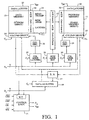
- a nonvolatile memory device of the present invention combines a program memory 11 with a data memory 13.
- the program memory 11 may be a flash memory array, which is meant to be initially programmed with program instruction codes and only infrequently updated (or not at all).
- the data memory 13 may be an E 2 PROM array which is programmed and more frequently updated with data parameters.
- the two memory arrays 11 and 13 need not be the same size and normally the program memory 11 is much larger than the data memory 13.
- the program memory 11 might be a 512K x 8 flash array (i.e., 4 Mbits) divided for write purposes into 2K 256-byte sectors, while the data memory 13 might be a 32K x 8 full-featured E 2 PROM capable of both single byte and 16-byte page writes.
- Other memory sizes and data widths are possible.
- the two memories 11 and 13 in the device share common address input lines A i , a considerable amount of address decoding circuitry, in particular, a common row decoder 15, common data input/output lines D j , and considerable data circuitry, including shared sense amplifiers 17 and I/O buffer circuitry 19.
- Control signals for read or output enable OE and write enable WE are also shared, but there are separate chip enable signals CEF and CEE corresponding to the flash and E 2 PROM memory arrays 11 and 13.
- Control logic 21 for the device is essentially shared by both memory arrays. This degree of resource sharing enables a smaller device to be built with fewer pins required for the address and data, since unnecessary duplication of circuitry and signal paths is avoided. Yet the device is still capable of concurrent access to the two memory arrays 11 and 13. Concurrent access is achieved despite shared addressing and data resources by providing the data memory 13 with a number of latch circuits 23, 24 and 27, especially row address latches 24 that free up the shared row decoder 15 for use by the program memory 11 during write operations to
- the address inputs A i are received by address buffers 25, 27 and 29.
- the address buffer 27 may take the form of read-transparent latches to hold these address bits for the duration of a byte write cycle of the data memory.
- the latching function for the data memory column address could be made part of the column select circuitry 37 after decoding.
- the other address buffers 25 and 29 could also take the form of latching circuits or may be simple tristate buffers that hold the address signals only for as long as they remain asserted on the address input lines A i . In either case, all address buffers are enabled in response to control signals C 1 -C 3 from the control logic 21.
- the control logic 21 in turn derives its control signals C k from the signals CEE , CEF , OE and WE received from the input pins of the device.
- the row address buffer 25 is enabled by signal C 1 whenever either chip enable CEE or CEF (but not both) is active (low) and either output enable or write enable signal OE or WE (but not both) is also active (low).
- the column address buffer 27 for the data memory 13 is enabled by signal C 2 whenever the E 2 PROM chip enable signal CEE is active and either output enable or write enable signal OE or WE is also active.
- the column address buffer 29 for the program memory 11 is enabled by signal C 3 whenever the Flash memory chip enable signal CEF is active and either output enable or write enable signal OE or WE is also active.
- the address information is input into the buffers 23, 27, 29 on the falling edge of appropriate chip enable signal CEE or CEF and appropriate output enable or write enable signal OE or WE , whichever occurs last.
- the condition where both chip enable signals are low or both output and write enable signals are low is invalid and generates no control signals from the logic 21.
- the row address buffer 25 is assigned the bulk of the address bits, e.g. bits A4 to A14 corresponding to a sector of the 512K x 8 flash memory array 11 and a page of the 32K x 8 E 2 PROM array 13.
- the column address buffers 27 and 29 are assigned the remaining address bits, e.g. bits A0 to A3 of the E 2 PROM array, and bits A0 to A3 and A15 to A18 of the flash array. Other arrangements of row and column address bits are possible, depending on the size and configuration of the respective memory arrays.
- the address information is supplied by the buffers 25, 27 and 29 to address decoding circuitry 15, 31 and 33.
- address decoding is carried out in two or more stages, including a first pre-decoding stage followed by a final decoding stage. For simplicity, all stages have been shown lumped together in Fig. 1 into corresponding single decoder circuits 15, 31, and 33.
- the shared row decoder 15 connects to both memory arrays 11 and 13. In the case of the program memory 11, the row decoder 15 communicates directly with row drivers 32 that activate a selected word line or row corresponding to the decoded row address bits. In the case of the data memory 13, the row decoder 15 connects to a read-transparent latching circuit 24.
- the latch circuit 24 in turn connects to row drivers 34 that activate a selected word line corresponding to the decoded row address received from the row decoder.
- the latch circuit 24 is effectively transparent so that the row decoder 15 communicates directly with the selected row driver.
- the latches 24 hold the decoded row address for writing to the data memory 13, so that the selected word line continues to be asserted with the programming voltage V pp .
- the column decoder 31 for the data memory 13 is connected to a column select circuit 35.
- the column decoder 33 for the program memory 11 is connected to a column select circuit 37.
- the column select circuits 35 and 37 are bidirectional multiplexing and gating circuits that control access of the data paths to a selected column of eight bit lines of the respective memory arrays 11 and 13.
- the operation of the select circuits 35 and 37 are controlled by signals C 4 and C 5 from the control logic 21.
- the selected column of bit lines corresponding to the column address in the enabled memory array 11 or 13 is connected to sense amplifiers 17.
- a data input/output buffer 19 responsive to another control signal C 6 outputs the sensed byte of data into the data lines D j .
- the enable column select circuit 35 or 37 (either CEE or CEF is low) connects the input/output buffer 19 to data latches 23 or 39 for the selected column of bit lines in the enabled memory array 11 or 13.
- Data received from the data lines D j J is loaded into the selected data latches 23 or 39 from which they can be loaded into the row and column of memory corresponding to the received and decoded address bits A i .
- the control logic 21 in addition to generating appropriate control signals C k in response to the input signals CEE , CEF , OE and WE , also controls generation of the high voltage V pp for programming data into the memory cells.
- the device may include JEDEC standard software data protection (W.P.).
- W.P. JEDEC standard software data protection
- each programming sequence for a sector of flash memory or a byte or page of the E 2 PROM must be preceded by a three-byte program command sequence in order for actual programming to take place. This sequence might consist of a specific combination of data bits D j and address bits A i , typically alternating zeros and ones.
- a write operation to the program memory begins with a three-byte write enable code to override the software write protection.
- the chip enable signal CEF for the flash memory and the write enable signal WE pulse low, while a sequence of three addresses and three corresponding sets of data are input into the device.
- address bits A18-A15 are ignored, since the write protect logic is also shared by the smaller E 2 PROM array 13. No actual writing to the flash memory occurs yet, but the sequence causes the control logic to begin allowing generation of a program voltage V pp and starts internal write timers.
- the flash memory is programmed in 256-byte sectors.
- a byte load is performed by applying a low pulse on CEF and WE with a CEE and OE high.
- the address is latched on the falling edge of CEF or WE whichever occurs last, while data is latched on the first rising edge of CEF or WE .
- the byte write cycle time typically is about 150 ⁇ s, although actual loads may take less time. After the first data byte has been programmed, successive bytes are entered in the same manner.
- Each new byte to be programmed must have its WE (or CEF ) high to low transition within 150 ⁇ s of the preceding bytes low to high transition of WE (or CEF ) or the load period will end.
- the total write cycle time for a sector of flash memory is typically about 10 ms. No read operations on the E 2 PROM array are allowed during flash memory's write period and attempts to read the flash memory will effectively be polling operations of the current byte being loaded.
- modifications to the device of Fig. 1 which include decoded row address latching circuits for the flash memory 11, as well as the E 2 PROM 13, would allow E 2 PROM reads during flash memory write operations, if desired.
- a flash memory read operation 52 occurs when the flash memory's chip enable signal CEF and the output enable signal OE pulse low, while CEE and WE remain high.
- the flash memory array 11 is read like a static RAM. Reading is carried out on individual bytes, rather than whole sectors. Moreover, for read operations the sectors appear seamless and sector boundaries need not be taken into account. That is, bytes from different sectors may be read successively.
- CEF and OE are low, the data DATA-OUT to be output that is stored at the flash memory location determined by the address inputs A 18 to A 0 is asserted on the data lines.
- the maximum read time is typically only 150 to 200 ns per byte.
- the E 2 PROM write operation 54 in Fig. 2 illustrates the capability provided by the memory architecture of the present invention of concurrently reading flash memory 11 during the write cycle period of the E 2 PROM array 13.
- Write protection is disabled by a 3-byte write enable code sequence, which is typically the same as that for the flash memory, except that now CEE pulses low, while CEF remains high.
- Read operations from the flash memory may interrupt loading of the write enable code sequence, as shown, provided the byte load cycle time of 150 ⁇ s is not violated. Since a read operation generally takes less than 200 ns to complete, there can be many bytes read from the flash memory between each byte of the code sequence.
- the write cycle is initiated by both CEE and WE going low. Once again, the address is latched by the falling edge of CEE or WE whichever occurs last, while data is latched into latches 23 of Fig. 1 on the rising edge of CEE or WE whichever occurs first.
- All write operations to the E 2 PROM array must conform to the limits of a page write. That is, while anywhere from a single byte of data to up to sixteen bytes of data may be written, all such bytes during a write cycle must reside on the same page, as defined by the address bits A14-A4. For each high to low transition of the signal WE , the bits A14-A4 must be the same (PAGE in Fig. 2). The A3 to A0 address bits are used to specify which bytes within the page are to be written. Address bits A18 to A15 do not apply to the smaller E 2 PROM array and will be ignored. For an entire page write operation, the bytes are normally written sequentially as indicated in Fig.
- Reads 56 from the flash memory array are allowed throughout the E 2 PROM write cycle time (up to 10 ms) so long as the byte load cycle time of 150 ⁇ s for the E 2 PROM write is not violated.
- a flash memory read occurs when CEF and OE pulse low.
- the data (BYTE) stored at the flash memory location (F.ADDR) determined by the address inputs A18 to A0 will be sensed and output on the data lines. Many reads can be performed in the time available. Attempts to read the E 2 PROM array ( CEE and OE low) during the E 2 PROM write cycle will produce a polling operation of the data held in the latches 23.
- the data (BYTE) stored at the memory location (E 2 ADDR.) determined by the address inputs A14-A0 will be sensed and output onto the data lines.
- An E 2 PROM read cannot be performed during any of the write cycles.
- the device of the present invention is intended to be used to store infrequently updated program information in one memory array and more frequently updated data parameters in another memory array.
- the architecture allows concurrent reading of the program memory during writes to the data memory, while eliminating much duplication in addressing and data hardware.
- the data memory's address latches free up the row decoder for performing read operation decoding for the program memory during the time period when data held in the data memory's data latches are actually programmed into memory cells. Thus, only one row decoder is needed.
- Alternative devices could have both memory arrays with independent address latches and drivers, so that read operations can be performed in either memory array while the other is completing a write operation. Only a single set of data and address inputs are needed for read and write of both arrays.
Landscapes
- Engineering & Computer Science (AREA)
- Computer Hardware Design (AREA)
- Read Only Memory (AREA)
Claims (10)
- Dispositif de mémoire non volatile, comprenant :une première matrice de mémoire non volatile (13),une seconde matrice de mémoire non volatile (11),une seule série de lignes d'adresse (Ai), dont au moins une partie est commune aux deux matrices de mémoire (11, 13),des moyens de sélection et de décodage d'adresse (15, 25, 27, 29, 35, 37) connectés aux dites lignes d'adresse (Ai) pour recevoir des signaux d'adresse provenant de ces dernières afin d'accéder à un emplacement de la mémoire dans l'une desdites matrices de mémoire (11, 13) sélectionnée, lesdits moyens de sélection et de décodage d'adresse comprenant :un décodeur de ligne partagé (15) commun aux deux matrices de mémoire pour accéder dans les deux matrices de mémoire à une ligne de mot(s) correspondant aux dits signaux d'adresse,un premier décodeur de colonne (31) et un premier circuit de sélection de colonne (35) couplés à ladite première matrice de mémoire (13), etun second décodeur de colonne (33) et un second circuit de sélection de colonne (37) couplés à ladite seconde matrice de mémoire (11),une seule série de lignes de données (Dj) commune aux deux matrices de mémoire (11, 13),une seule série d'amplificateurs de détection (17) commune aux deux matrices de mémoire (11, 13) et pouvant communiquer au moyen desdits moyens de sélection et de décodage d'adresse avec des lignes de bits sélectionnées correspondant aux emplacements adressés de ladite matrice de mémoire sélectionnée, lesdits amplificateurs de détection (17) connectant lesdites lignes de bits sélectionnées aux dites lignes de données (Dj) pour une opération de lecture de ladite matrice de mémoire sélectionnée,des premier et second moyens de verrouillage (23, 39) pouvant être connectés au moyen desdits moyens de sélection et de décodage d'adresse à ladite seule série de lignes de données (Dj) et aux lignes de bits desdites première et seconde matrices de mémoire respectives (11, 13) pour conserver des données reçues desdites lignes de données pendant une opération d'écriture vers ladite matrice de mémoire sélectionnée, etdes moyens de commande (21) réceptifs à des signaux de commande d'entrée (CEE, CEF, OE, WE) pour sélectionner l'une desdites matrices de mémoire (11, 13) et sélectionner une opération de lecture ou d'écriture pour ladite matrice de mémoire sélectionnée, caractérisés par la fourniture de moyens de verrouillage d'adresse (24), couplés à ladite première matrice de mémoire (13) et en communication avec lesdits moyens de décodage d'adresse, qui conservent une adresse décodée par le décodeur de ligne (15) pendant une opération d'écriture vers ladite première matrice de mémoire, moyennant quoi lesdits moyens de sélection et de décodage d'adresse sont libres d'accéder à d'autres emplacements de la mémoire pour des opérations de lecture simultanées à partir de ladite seconde matrice de mémoire (11).
- Dispositif de mémoire selon la revendication 1 dans lequel ladite première matrice de mémoire (13) est une matrice d'E2PROM.
- Dispositif selon la revendication 2 dans lequel ladite matrice d'E2PROM possède des fonctionnalités d'écriture sur un seul octet et en mode page.
- Dispositif de mémoire selon la revendication 1, 2 ou 3, dans lequel ladite seconde matrice de mémoire (11) est une matrice de mémoire flash.
- Dispositif de mémoire selon l'une quelconque des revendications précédentes, dans lequel lesdits moyens de verrouillage d'adresse (24) pour ladite première matrice de mémoire (13) sont en réalité transparents pendant une opération de lecture de ladite première matrice de mémoire (11) et isolent ladite adresse décodée et conservée desdits moyens de sélection et de décodage d'adresse jusqu'à la fin d'une opération d'écriture pour ladite première matrice de mémoire (13).
- Dispositif de mémoire selon la revendication 1 comprenant en outre des seconds moyens de verrouillage d'adresse couplés à ladite seconde matrice de mémoire (11) pour conserver une adresse décodée pendant une opération d'écriture pour ladite seconde matrice de mémoire.
- Dispositif de mémoire selon la revendication 1, dans lequel lesdites matrices de mémoire (11, 13) possèdent des tailles différentes, la plus grande desdites matrices de mémoire nécessitant toutes lesdites lignes d'adresse (Ai) pour accéder aux emplacements sélectionnés de cette matrice de mémoire plus grande, la plus petite desdites matrices de mémoire nécessitant uniquement une série secondaire desdites lignes d'adresse pour accéder aux emplacements sélectionnés de cette matrice de mémoire plus petite.
- Dispositif selon la revendication 7 dans lequel ladite seconde matrice de mémoire (11) possède une capacité de mémoire plus grande que ladite première matrice de mémoire (13), ladite seconde matrice de mémoire nécessitant toutes les lignes d'adresse (Ai) pour y accéder, ladite première matrice de mémoire requérant moins que toutes les lignes d'adresse pour accéder à cette dernière.
- Dispositif de mémoire selon l'une quelconque des revendications précédentes, dans lequel lesdits signaux de commande d'entrée (CEE, CEF, OE, WE) comprennent une première série de signaux sélectionnant une et seulement une desdites matrices de mémoire (11, 13) et une seconde série de signaux permettant une et seulement une opération de lecture ou d'écriture.
- Dispositif selon la revendication 1 dans lequel lesdits premier et second circuits de sélection et de décodage de colonne (31, 33, 35, 37) comprennent des circuits portes directionnels pour connecter les lignes de bits sélectionnées aux dits amplificateurs de détection (17) pour une opération de lecture et pour connecter lesdites lignes de données (Dj) aux verrous de données correspondant aux lignes de bit sélectionnées pour une opération d'écriture.
Applications Claiming Priority (3)
| Application Number | Priority Date | Filing Date | Title |
|---|---|---|---|
| US829378 | 1997-03-31 | ||
| US08/829,378 US5732017A (en) | 1997-03-31 | 1997-03-31 | Combined program and data nonvolatile memory with concurrent program-read/data write capability |
| PCT/US1998/001305 WO1998044511A1 (fr) | 1997-03-31 | 1998-01-22 | Memoire non volatile combinee programme et donnees permettant une lecture de programme et une ecriture de donnees concurrentes |
Publications (3)
| Publication Number | Publication Date |
|---|---|
| EP0914659A1 EP0914659A1 (fr) | 1999-05-12 |
| EP0914659A4 EP0914659A4 (fr) | 2002-01-23 |
| EP0914659B1 true EP0914659B1 (fr) | 2005-01-12 |
Family
ID=25254375
Family Applications (1)
| Application Number | Title | Priority Date | Filing Date |
|---|---|---|---|
| EP98903669A Expired - Lifetime EP0914659B1 (fr) | 1997-03-31 | 1998-01-22 | Memoire non volatile combinee programme et donnees permettant une lecture de programme et une ecriture de donnees concurrentes |
Country Status (7)
| Country | Link |
|---|---|
| US (1) | US5732017A (fr) |
| EP (1) | EP0914659B1 (fr) |
| JP (1) | JP2001526819A (fr) |
| CN (1) | CN1195303C (fr) |
| DE (1) | DE69828564T2 (fr) |
| TW (1) | TW459232B (fr) |
| WO (1) | WO1998044511A1 (fr) |
Families Citing this family (42)
| Publication number | Priority date | Publication date | Assignee | Title |
|---|---|---|---|---|
| US5661677A (en) | 1996-05-15 | 1997-08-26 | Micron Electronics, Inc. | Circuit and method for on-board programming of PRD Serial EEPROMS |
| US5901086A (en) * | 1996-12-26 | 1999-05-04 | Motorola, Inc. | Pipelined fast-access floating gate memory architecture and method of operation |
| JPH10326493A (ja) * | 1997-05-23 | 1998-12-08 | Ricoh Co Ltd | 複合化フラッシュメモリ装置 |
| FR2771839B1 (fr) * | 1997-11-28 | 2000-01-28 | Sgs Thomson Microelectronics | Memoire non volatile programmable et effacable electriquement |
| US6032248A (en) * | 1998-04-29 | 2000-02-29 | Atmel Corporation | Microcontroller including a single memory module having a data memory sector and a code memory sector and supporting simultaneous read/write access to both sectors |
| US6091620A (en) * | 1999-07-06 | 2000-07-18 | Virage Logic Corporation | Multi-bank memory with word-line banking, bit-line banking and I/O multiplexing utilizing tilable interconnects |
| JP3530425B2 (ja) * | 1999-08-20 | 2004-05-24 | Necマイクロシステム株式会社 | 半導体記憶装置 |
| US6178132B1 (en) * | 1999-09-09 | 2001-01-23 | Macronix International Co., Ltd. | Non-volatile integrated circuit having read while write capability using one address register |
| US6851026B1 (en) | 2000-07-28 | 2005-02-01 | Micron Technology, Inc. | Synchronous flash memory with concurrent write and read operation |
| JP2001344986A (ja) * | 2000-06-05 | 2001-12-14 | Mitsubishi Electric Corp | 不揮発性半導体記憶装置 |
| US6883044B1 (en) * | 2000-07-28 | 2005-04-19 | Micron Technology, Inc. | Synchronous flash memory with simultaneous access to one or more banks |
| US6552935B2 (en) | 2001-08-02 | 2003-04-22 | Stmicroelectronics, Inc. | Dual bank flash memory device and method |
| US6728159B2 (en) * | 2001-12-21 | 2004-04-27 | International Business Machines Corporation | Flexible multibanking interface for embedded memory applications |
| CN100336133C (zh) * | 2002-02-10 | 2007-09-05 | 台湾积体电路制造股份有限公司 | 隐藏式更新存储器功能的1-t存储器结构及其操作方法 |
| JP2003263421A (ja) * | 2002-03-07 | 2003-09-19 | Mitsubishi Electric Corp | マイクロコンピュータ |
| US6799256B2 (en) * | 2002-04-12 | 2004-09-28 | Advanced Micro Devices, Inc. | System and method for multi-bit flash reads using dual dynamic references |
| US8108588B2 (en) * | 2003-04-16 | 2012-01-31 | Sandisk Il Ltd. | Monolithic read-while-write flash memory device |
| JP4350431B2 (ja) * | 2003-06-10 | 2009-10-21 | パナソニック株式会社 | 半導体メモリ装置 |
| US7184315B2 (en) * | 2003-11-04 | 2007-02-27 | Micron Technology, Inc. | NROM flash memory with self-aligned structural charge separation |
| US7092288B2 (en) * | 2004-02-04 | 2006-08-15 | Atmel Corporation | Non-volatile memory array with simultaneous write and erase feature |
| JP2005332502A (ja) * | 2004-05-20 | 2005-12-02 | Renesas Technology Corp | 半導体装置およびicカード |
| JP4795660B2 (ja) * | 2004-09-29 | 2011-10-19 | ルネサスエレクトロニクス株式会社 | 半導体装置 |
| US7200049B2 (en) | 2004-11-18 | 2007-04-03 | Samsung Electronics Co., Ltd. | Methods for accelerated erase operations in non-volatile memory devices and related devices |
| TWI290302B (en) * | 2005-02-02 | 2007-11-21 | Mitac Int Corp | Recording card for flash memory |
| US7206230B2 (en) * | 2005-04-01 | 2007-04-17 | Sandisk Corporation | Use of data latches in cache operations of non-volatile memories |
| CN1963787A (zh) * | 2005-11-10 | 2007-05-16 | 其乐达科技股份有限公司 | 嵌入式系统的快闪存储器存取方法及存取电路 |
| JP2007141286A (ja) * | 2005-11-15 | 2007-06-07 | Nec Electronics Corp | 半導体集積回路装置及びその制御方法 |
| US7558907B2 (en) * | 2006-10-13 | 2009-07-07 | Spansion Llc | Virtual memory card controller |
| WO2009079478A1 (fr) * | 2007-12-14 | 2009-06-25 | Virident Systems, Inc. | Distribution de métadonnées au sein de différentes zones de rupture dans un système de mémoire asymétrique |
| CN101694780B (zh) * | 2009-10-14 | 2012-04-18 | 上海宏力半导体制造有限公司 | 存储阵列结构、嵌入式存储器及系统级芯片 |
| DE102010028231A1 (de) * | 2010-04-27 | 2011-10-27 | Robert Bosch Gmbh | Speichermodul zur gleichzeitigen Bereitstellung wenigstens eines sicheren und wenigstens eines unsicheren Speicherbereichs |
| JP2012198965A (ja) * | 2011-03-22 | 2012-10-18 | Toshiba Corp | 不揮発性半導体記憶装置 |
| TWI587142B (zh) * | 2012-11-23 | 2017-06-11 | 普誠科技股份有限公司 | 介面傳輸方法以及資料結構產品 |
| US9502125B2 (en) * | 2014-09-08 | 2016-11-22 | Micron Technology, Inc. | Concurrently reading first and second pages of memory cells having different page addresses |
| TWI626658B (zh) * | 2016-06-14 | 2018-06-11 | 旺宏電子股份有限公司 | 記憶體裝置及其操作方法 |
| US10115441B1 (en) | 2017-07-20 | 2018-10-30 | Macronix International Co., Ltd. | Row decoder and memory system using the same |
| CN109390006B (zh) * | 2017-08-10 | 2021-06-29 | 旺宏电子股份有限公司 | 列译码器及应用其的存储器系统 |
| TWI630616B (zh) * | 2017-08-11 | 2018-07-21 | 旺宏電子股份有限公司 | 列解碼器及應用其之記憶體系統 |
| US10607659B2 (en) * | 2018-04-23 | 2020-03-31 | Arm Limited | Method, system and device for integration of bitcells in a volatile memory array and bitcells in a non-volatile memory array |
| DE102021107045B4 (de) | 2021-03-10 | 2024-11-21 | Elmos Semiconductor Se | Rechnersystem für eine Motorsteuerung mit einem Programmspeicher und einem Datenspeicher |
| US12176038B2 (en) * | 2022-08-18 | 2024-12-24 | Yangtze Memory Technologies Co., Ltd. | Memory device and read operation during suspension of program operation thereof |
| CN118245402A (zh) | 2022-12-22 | 2024-06-25 | 长江存储科技有限责任公司 | 提高多逻辑单元(lun)操作效率的总线间插协议 |
Family Cites Families (12)
| Publication number | Priority date | Publication date | Assignee | Title |
|---|---|---|---|---|
| US3471838A (en) * | 1965-06-21 | 1969-10-07 | Magnavox Co | Simultaneous read and write memory configuration |
| JP2654215B2 (ja) * | 1990-01-19 | 1997-09-17 | 株式会社東芝 | 半導体メモリシステム |
| JP3532932B2 (ja) * | 1991-05-20 | 2004-05-31 | モトローラ・インコーポレイテッド | 時間重複メモリ・アクセスを有するランダムにアクセス可能なメモリ |
| US5307314A (en) * | 1991-07-15 | 1994-04-26 | Micron Technology, Inc. | Split read/write dynamic random access memory |
| US5245572A (en) * | 1991-07-30 | 1993-09-14 | Intel Corporation | Floating gate nonvolatile memory with reading while writing capability |
| US5420997A (en) * | 1992-01-02 | 1995-05-30 | Browning; Gary A. | Memory having concurrent read and writing from different addresses |
| US5369609A (en) * | 1992-03-13 | 1994-11-29 | Silicon Storage Technology, Inc. | Floating gate memory array with latches having improved immunity to write disturbance, and with storage latches |
| JPH05275657A (ja) * | 1992-03-26 | 1993-10-22 | Toshiba Corp | 半導体記憶装置 |
| US5502683A (en) * | 1993-04-20 | 1996-03-26 | International Business Machines Corporation | Dual ported memory with word line access control |
| US5436863A (en) * | 1993-04-26 | 1995-07-25 | Nec Corporation | Semiconductor memory device |
| FR2719939A1 (fr) * | 1994-05-11 | 1995-11-17 | Sgs Thomson Microelectronics | Mémoire non volatile modifiable électriquement à interface de commande. |
| US5513139A (en) * | 1994-11-04 | 1996-04-30 | General Instruments Corp. | Random access memory with circuitry for concurrently and sequentially writing-in and reading-out data at different rates |
-
1997
- 1997-03-31 US US08/829,378 patent/US5732017A/en not_active Expired - Lifetime
-
1998
- 1998-01-22 EP EP98903669A patent/EP0914659B1/fr not_active Expired - Lifetime
- 1998-01-22 DE DE69828564T patent/DE69828564T2/de not_active Expired - Fee Related
- 1998-01-22 JP JP53574898A patent/JP2001526819A/ja active Pending
- 1998-01-22 CN CNB988000067A patent/CN1195303C/zh not_active Expired - Fee Related
- 1998-01-22 WO PCT/US1998/001305 patent/WO1998044511A1/fr not_active Ceased
- 1998-02-03 TW TW087101272A patent/TW459232B/zh not_active IP Right Cessation
Also Published As
| Publication number | Publication date |
|---|---|
| EP0914659A4 (fr) | 2002-01-23 |
| EP0914659A1 (fr) | 1999-05-12 |
| CN1216141A (zh) | 1999-05-05 |
| TW459232B (en) | 2001-10-11 |
| JP2001526819A (ja) | 2001-12-18 |
| WO1998044511A1 (fr) | 1998-10-08 |
| US5732017A (en) | 1998-03-24 |
| DE69828564D1 (de) | 2005-02-17 |
| DE69828564T2 (de) | 2005-12-29 |
| CN1195303C (zh) | 2005-03-30 |
| HK1018658A1 (en) | 1999-12-30 |
Similar Documents
| Publication | Publication Date | Title |
|---|---|---|
| EP0914659B1 (fr) | Memoire non volatile combinee programme et donnees permettant une lecture de programme et une ecriture de donnees concurrentes | |
| US6016270A (en) | Flash memory architecture that utilizes a time-shared address bus scheme and separate memory cell access paths for simultaneous read/write operations | |
| US5606532A (en) | EEPROM array with flash-like core | |
| US6542956B1 (en) | Latched address multi-chunk write to EEPROM | |
| US5280594A (en) | Architecture for high speed contiguous sequential access memories | |
| US5361343A (en) | Microprocessor system including first and second nonvolatile memory arrays which may be simultaneously read and reprogrammed | |
| US5297029A (en) | Semiconductor memory device | |
| US6580659B1 (en) | Burst read addressing in a non-volatile memory device | |
| US7227777B2 (en) | Mode selection in a flash memory device | |
| US5737258A (en) | Nonvolatile semiconductor memory which is connectable to a DRAM bus | |
| US5504875A (en) | Nonvolatile memory with a programmable output of selectable width and a method for controlling the nonvolatile memory to switch between different output widths | |
| EP0374829B1 (fr) | Unité de mémoire à double porte | |
| US7051178B2 (en) | Burst write in a non-volatile memory device | |
| US6215705B1 (en) | Simultaneous program, program-verify scheme | |
| US5285421A (en) | Scheme for eliminating page boundary limitation on initial access of a serial contiguous access memory | |
| US6515900B2 (en) | Non-volatile memory with background operation function | |
| US6507514B1 (en) | Integrated circuit memory chip for use in single or multi-chip packaging | |
| US5493241A (en) | Memory having a decoder with improved address hold time | |
| EP1137011B1 (fr) | Mémoire non-volatile à structure NOR programmable par séquences de mots | |
| US7305514B2 (en) | Command sequence for optimized power consumption | |
| US6160750A (en) | Noise reduction during simultaneous operation of a flash memory device | |
| KR100365690B1 (ko) | 불휘발성 메모리, 복수개의 불휘발성 메모리들을 구비한시스템 , 및 이 시스템의 데이터 리드 방법 | |
| KR100480653B1 (ko) | 프로그램판독/데이터기록을동시에수행하는능력을갖는결합된프로그램및데이터비휘발성메모리 | |
| US6622201B1 (en) | Chained array of sequential access memories enabling continuous read | |
| WO1992020068A1 (fr) | Systeme de memoire rapide utilisant des memoires pour la plupart bonnes |
Legal Events
| Date | Code | Title | Description |
|---|---|---|---|
| PUAI | Public reference made under article 153(3) epc to a published international application that has entered the european phase |
Free format text: ORIGINAL CODE: 0009012 |
|
| 17P | Request for examination filed |
Effective date: 19980930 |
|
| AK | Designated contracting states |
Kind code of ref document: A1 Designated state(s): DE FR GB IT NL |
|
| A4 | Supplementary search report drawn up and despatched |
Effective date: 20011211 |
|
| AK | Designated contracting states |
Kind code of ref document: A4 Designated state(s): DE FR GB IT NL |
|
| RIC1 | Information provided on ipc code assigned before grant |
Free format text: 7G 11C 16/04 A, 7G 11C 11/00 B, 7G 11C 16/10 B, 7G 11C 16/26 B |
|
| 17Q | First examination report despatched |
Effective date: 20030602 |
|
| GRAP | Despatch of communication of intention to grant a patent |
Free format text: ORIGINAL CODE: EPIDOSNIGR1 |
|
| GRAS | Grant fee paid |
Free format text: ORIGINAL CODE: EPIDOSNIGR3 |
|
| GRAA | (expected) grant |
Free format text: ORIGINAL CODE: 0009210 |
|
| AK | Designated contracting states |
Kind code of ref document: B1 Designated state(s): DE FR GB IT NL |
|
| REG | Reference to a national code |
Ref country code: GB Ref legal event code: FG4D |
|
| PGFP | Annual fee paid to national office [announced via postgrant information from national office to epo] |
Ref country code: NL Payment date: 20050131 Year of fee payment: 8 |
|
| REF | Corresponds to: |
Ref document number: 69828564 Country of ref document: DE Date of ref document: 20050217 Kind code of ref document: P |
|
| ET | Fr: translation filed | ||
| PLBE | No opposition filed within time limit |
Free format text: ORIGINAL CODE: 0009261 |
|
| STAA | Information on the status of an ep patent application or granted ep patent |
Free format text: STATUS: NO OPPOSITION FILED WITHIN TIME LIMIT |
|
| 26N | No opposition filed |
Effective date: 20051013 |
|
| PG25 | Lapsed in a contracting state [announced via postgrant information from national office to epo] |
Ref country code: NL Free format text: LAPSE BECAUSE OF NON-PAYMENT OF DUE FEES Effective date: 20060801 |
|
| NLV4 | Nl: lapsed or anulled due to non-payment of the annual fee |
Effective date: 20060801 |
|
| PGFP | Annual fee paid to national office [announced via postgrant information from national office to epo] |
Ref country code: IT Payment date: 20080129 Year of fee payment: 10 |
|
| PGFP | Annual fee paid to national office [announced via postgrant information from national office to epo] |
Ref country code: DE Payment date: 20090302 Year of fee payment: 12 |
|
| PGFP | Annual fee paid to national office [announced via postgrant information from national office to epo] |
Ref country code: GB Payment date: 20090129 Year of fee payment: 12 |
|
| PG25 | Lapsed in a contracting state [announced via postgrant information from national office to epo] |
Ref country code: IT Free format text: LAPSE BECAUSE OF NON-PAYMENT OF DUE FEES Effective date: 20080122 |
|
| PGFP | Annual fee paid to national office [announced via postgrant information from national office to epo] |
Ref country code: FR Payment date: 20090119 Year of fee payment: 12 |
|
| GBPC | Gb: european patent ceased through non-payment of renewal fee |
Effective date: 20100122 |
|
| REG | Reference to a national code |
Ref country code: FR Ref legal event code: ST Effective date: 20100930 |
|
| PG25 | Lapsed in a contracting state [announced via postgrant information from national office to epo] |
Ref country code: FR Free format text: LAPSE BECAUSE OF NON-PAYMENT OF DUE FEES Effective date: 20100201 |
|
| PG25 | Lapsed in a contracting state [announced via postgrant information from national office to epo] |
Ref country code: DE Free format text: LAPSE BECAUSE OF NON-PAYMENT OF DUE FEES Effective date: 20100803 |
|
| PG25 | Lapsed in a contracting state [announced via postgrant information from national office to epo] |
Ref country code: GB Free format text: LAPSE BECAUSE OF NON-PAYMENT OF DUE FEES Effective date: 20100122 |