EP0915566A2 - Rücksetzschaltung für Flipflop - Google Patents
Rücksetzschaltung für Flipflop Download PDFInfo
- Publication number
- EP0915566A2 EP0915566A2 EP98121123A EP98121123A EP0915566A2 EP 0915566 A2 EP0915566 A2 EP 0915566A2 EP 98121123 A EP98121123 A EP 98121123A EP 98121123 A EP98121123 A EP 98121123A EP 0915566 A2 EP0915566 A2 EP 0915566A2
- Authority
- EP
- European Patent Office
- Prior art keywords
- clock
- flipflop
- power
- reset
- circuit
- Prior art date
- Legal status (The legal status is an assumption and is not a legal conclusion. Google has not performed a legal analysis and makes no representation as to the accuracy of the status listed.)
- Withdrawn
Links
Images


Classifications
-
- H—ELECTRICITY
- H03—ELECTRONIC CIRCUITRY
- H03K—PULSE TECHNIQUE
- H03K3/00—Circuits for generating electric pulses; Monostable, bistable or multistable circuits
- H03K3/02—Generators characterised by the type of circuit or by the means used for producing pulses
- H03K3/027—Generators characterised by the type of circuit or by the means used for producing pulses by the use of logic circuits, with internal or external positive feedback
- H03K3/037—Bistable circuits
- H03K3/0375—Bistable circuits provided with means for increasing reliability; for protection; for ensuring a predetermined initial state when the supply voltage has been applied; for storing the actual state when the supply voltage fails
-
- H—ELECTRICITY
- H03—ELECTRONIC CIRCUITRY
- H03K—PULSE TECHNIQUE
- H03K17/00—Electronic switching or gating, i.e. not by contact-making and –breaking
- H03K17/22—Modifications for ensuring a predetermined initial state when the supply voltage has been applied
Definitions
- the present invention relates to a reset circuit, and more specifically to a reset circuit for a flipflop.
- this type of reset circuit has been used in a processor having a data bus, in order to prevent a pass-through current occurring due to a logic collision on a bus caused because the output value of bus controlling flipflops are indefinite at a power-on time.
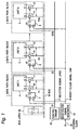
- FIG. 6 there is shown a block diagram of one example of the prior art reset circuit.
- a plurality of data path blocks 1, 2 and 3 are connected to the same bus 16, which is connected with a bus latch 32.
- These data path blocks are the same in a connection fashion with the bus and in an internal construction. Therefore, the data path block 3 will be described in detail.
- a data path unit 6 has data output terminals connected to tristate buffers 14 and 15, respectively, and data input terminals connected to the data bus 16.
- the tristate buffers are of the same number as a bit width of the data bus 16. Here, it is assumed that the bit width of the data bus 16 is 2 for simplification of description and drawings.
- An output of the tristate buffers is connected to the data bus 16.
- a control terminal of the tristate buffers 14 and 15 is connected to an output of a flipflop circuit (abbreviated to "FF" in the drawings) 31.
- a data input terminal of the flipflop 31 is connected to one corresponding signal line of selection signal lines 17, and a clock terminal of the flipflop 31 is connected to a clock signal line 20.
- a reset terminal of the flipflop 31 is connected to a reset signal line 25.
- a control circuit 19 has output terminals of the number corresponding to the number of data path blocks connected to the bus. The output terminals of the control circuit 19 are connected to the selection signal lines 17, respectively.
- the reset signal line 25 is connected to an output of a power-on-reset circuit 23.
- each flipflop since the reset terminal of each flipflop is supplied with the power-on-reset signal, each flipflop is reset at the power-on time, so that the output of each flipflop becomes "0", with the result that the output of all the tristates connected to the bus become a high impedance, and therefore, the bus is held at the value of the bus latch 32. Furthermore, if the external clock is inputted, the value of each flipflop becomes a value reflecting the corresponding output of the control circuit 19, so that the bus is driven with only one unit.
- the above mentioned prior art reset circuit has a problem in which the flipflop having the reset function, of the number equal to the number of the units, are required, and in addition, it is necessary to lay out the reset signal line. This results in an increased circuit scale, and in an increased occupying area when the circuit is incorporated in an LSI (large scale integrated circuit.
- Another object of the present invention is to provide a reset circuit for a flipflop, capable of preventing the value of the flipflop from being indefinite during a period from a power-on time to the time a first clock signal is inputted.
- a reset circuit for a flipflop comprising:
- the clock generating means is a reset clock generating circuit for generating a reset clock at the power-on time, the reset clock being supplied to the clock input terminal of the flipflop by the clock supplying means.
- the clock supplying means includes a power-on-reset circuit for generating a power-on-reset signal having a predetermined active period of time at the power-on time, and a selector circuit for supplying the internal clock generated by the clock generating means, to the clock input terminal of the flipflop during a period of time in which the power-on-reset signal is active, the selector circuit supplying the external clock to the clock input terminal of the flipflop after the power-on-reset signal is rendered inactive.
- the clock generating means can be constituted of a ring oscillator.
- the clock supplying means includes a power-on-reset circuit for generating a power-on-reset signal having a predetermined active period of time at the power-on time, and an OR gate receiving the power-on-reset signal and the external clock for supplying the power-on-reset signal to the clock input terminal of the flipflop during a period of time in which the power-on-reset signal is activated at a high level, and for supplying the external clock to the clock input terminal of the flipflop after the power-on-reset signal is deactivated to a low level.
- the clock generating means can be constituted of the power-on-reset circuit.
- the flipflop is a flipflop having no reset input terminal
- the reset circuit for the flipflop in accordance with the present invention comprises the clock generating means and the clock supplying means for supplying the clock to the clock input terminal of the flipflop at the power-on time. Therefore, since the clock input terminal of the flipflop is supplied with the clock at the power-on time, an output of the flipflop never becomes indefinite. For example, in the case that an input/output of tristate buffers connected in common to the same bus are controlled by a corresponding number of flipflops, respectively, a pass-through current caused for an output collision on the bus can be prevented with a relatively small scale of circuit.
- FIG. 1 there is shown a block diagram of an embodiment of the reset circuit in accordance with the present invention.
- elements corresponding to those shown in Fig. 6 are given the same Reference Numerals, and explanation will be omitted.
- flipflops 7 to 9 having no reset input terminal are provided in place of the flipflops 29 to 31, and therefore, the reset signal line 25 is omitted.
- a clock input terminal of the flipflops 7 to 9 is connected to a reset/clock signal line 18 connected to an output of a reset/clock signal generator 21.
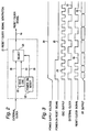
- FIG. 2 An example of a detailed construction of this reset/clock signal generator 21 is shown in Fig. 2.
- Reference Numeral 22 designates a self-running oscillator such as a ring oscillator, and Reference Numeral 23 denotes a power-on-reset circuit.
- Reference Numeral 20 shows an external clock signal line, and Reference Numeral 26 indicates a selector for selecting either the external clock signal 20 or an internal clock 24 generated in the internal oscillator 22. This selector 26 is controlled by an output signal 25 of the power-on-reset circuit 23.
- Fig. 3 is a timing chart for illustrating an operation of the reset circuit in accordance with the present invention having the reset/clock signal generator shown in Fig. 2.
- Reference Numeral 28 indicates a change of a power supply voltage.
- Reference Numeral 25 designates the output of the power-on-reset circuit 23.
- Reference Numeral 24 denotes an output of the internal oscillator 22.
- Reference Numeral 20 shows the external clock signal.
- Reference Numeral 18 designates the reset/clock signal outputted from the selector 26.
- Reference Numeral 29 denotes an output of the flipflops 7 to 9. As seen from the waveform of the power supply voltage, Fig.
- the power-on-reset signal 25 of a high level is outputted during a constant period of time determined by a time constant of an internal circuit of the power-on-reset circuit.
- the selector 26 When the active power-on-reset signal 25 (of the high level) is outputted, the selector 26 is controlled to select the output 24 of the internal oscillator 23, and therefore, the output 24 of the internal oscillator 23 is outputted as the output 18 of the reset/clock signal generator 21. Since this signal 18 is supplied to the clock input terminal of the flipflops 7 to 9, the output of the flipflops 7 to 9 becomes definite immediately after the power-on of the power supply voltage.
- the selector 26 is controlled to select the external clock signal 20, and therefore, the external clock signal 20 is outputted as the output 18 of the reset/clock signal generator 21. Thereafter, the flipflops 7 to 9 fetch the selection signals S1, S2, ⁇ ⁇ ⁇ S(N) from the control circuit 19 in synchronism with the clock signal 18.
- the reset circuit since the clock signal input terminal also acts as the reset signal input terminal, the reset circuit can be constructed with flipflops having no reset input terminal, differently from the prior art reset circuit, and therefore, the circuit scale and the scale of the wiring for supplying the signals can be greatly reduced.
- the internal oscillator and the selector have to be added. However, if the internal oscillator is constructed of a ring oscillator, it can be constructed with a small number of gates. In addition, the selector can be constructed with a few gates at most. Accordingly, the reset circuit in accordance with the present invention has a remarkably great advantage in applications, such as microprocessor, having a large number of data path blocks connected to a bus.
- FIG. 4 there is shown a circuit diagram of another example of the reset/clock signal generator 21 in the embodiment of the reset circuit in accordance with the present invention.
- Reference Numeral 20 indicates the external clock signal 20.
- Reference Numeral 23 designates the power-on-reset circuit.
- Reference Numeral 27 denotes an OR gate. In this embodiment, the reset pulse generated in the power-on-reset circuit 23 is used as an internally generated clock.
- the reset clock signal 25 is outputted as it is through the OR gate 27 as the reset/clock signal 18.
- the external clock signal 20 is outputted as it is through the OR gate 27 as the reset/clock signal 18.
- the flipflops 7 to 9 are set to a predetermined condition in response to a rising edge of the reset pulse generated by the power-on-reset circuit 23 just after the power-on of the power supply voltage. Accordingly, no bus collision occurs which had occurred in the prior art because the output of the flipflops is indefinite just after the power-on of the power supply voltage.
- the reset circuit in accordance with the present invention includes a clock generating means and a means for supplying a clock to the clock input terminal of the flipflops at the power-on time. Therefore, since the clock is supplied to the clock input terminal of the flipflops at the power-on time, the output of the flipflops never becomes indefinite. For example, in the case that an input/output of a plurality of tristate buffers connected to the bus are controlled by an output of a corresponding number of flipflops, it is possible to prevent generation of the pass-through current caused by an output collision on the bus, by a circuit scale which is smaller than that of the prior art reset circuit.
Landscapes
- Electronic Switches (AREA)
Applications Claiming Priority (3)
| Application Number | Priority Date | Filing Date | Title |
|---|---|---|---|
| JP30726397A JP3368815B2 (ja) | 1997-11-10 | 1997-11-10 | フリップフロップ回路 |
| JP307263/97 | 1997-11-10 | ||
| JP30726397 | 1997-11-10 |
Publications (2)
| Publication Number | Publication Date |
|---|---|
| EP0915566A2 true EP0915566A2 (de) | 1999-05-12 |
| EP0915566A3 EP0915566A3 (de) | 2000-12-06 |
Family
ID=17967012
Family Applications (1)
| Application Number | Title | Priority Date | Filing Date |
|---|---|---|---|
| EP98121123A Withdrawn EP0915566A3 (de) | 1997-11-10 | 1998-11-10 | Rücksetzschaltung für Flipflop |
Country Status (6)
| Country | Link |
|---|---|
| US (1) | US6147537A (de) |
| EP (1) | EP0915566A3 (de) |
| JP (1) | JP3368815B2 (de) |
| KR (1) | KR100337722B1 (de) |
| CN (1) | CN1217609A (de) |
| TW (1) | TW437169B (de) |
Cited By (2)
| Publication number | Priority date | Publication date | Assignee | Title |
|---|---|---|---|---|
| WO2011051275A1 (en) | 2009-10-27 | 2011-05-05 | Solvay Fluor Gmbh | Lithium sulfur battery |
| WO2012146525A1 (en) | 2011-04-26 | 2012-11-01 | Solvay Sa | Lithium air battery cell |
Families Citing this family (9)
| Publication number | Priority date | Publication date | Assignee | Title |
|---|---|---|---|---|
| KR100336753B1 (ko) * | 1999-08-06 | 2002-05-16 | 박종섭 | 상태 클럭 발생기 |
| US7038506B2 (en) * | 2004-03-23 | 2006-05-02 | Stmicroelectronics Pvt. Ltd. | Automatic selection of an on-chip ancillary internal clock generator upon resetting a digital system |
| US7148118B2 (en) * | 2004-07-08 | 2006-12-12 | Micron Technology, Inc. | Methods of forming metal nitride, and methods of forming capacitor constructions |
| JP4549935B2 (ja) * | 2005-06-10 | 2010-09-22 | 三菱電機株式会社 | 半導体集積回路設計支援システム及びプログラム |
| JP4749813B2 (ja) * | 2005-09-21 | 2011-08-17 | 三菱電機株式会社 | 半導体集積回路設計支援システム及びプログラム |
| KR100703711B1 (ko) | 2006-01-14 | 2007-04-09 | 삼성전자주식회사 | 데이터 전송 버퍼의 동작을 제어하기 위한 제어신호발생장치, 상기 제어신호 발생장치를 구비하는 반도체장치, 및 상기 전송 버퍼의 동작을 제어하는 방법 |
| KR101062778B1 (ko) * | 2010-05-31 | 2011-09-06 | 주식회사 하이닉스반도체 | 파워업 신호 생성 장치 및 파워업 신호 생성 방법 |
| US8890588B2 (en) * | 2013-03-28 | 2014-11-18 | Texas Instruments Incorporated | Circuits and methods for asymmetric aging prevention |
| JP7271264B2 (ja) * | 2019-03-29 | 2023-05-11 | ラピスセミコンダクタ株式会社 | ラッチアレイ回路及び半導体集積回路 |
Family Cites Families (7)
| Publication number | Priority date | Publication date | Assignee | Title |
|---|---|---|---|---|
| JP3105510B2 (ja) * | 1989-07-21 | 2000-11-06 | 日本電気株式会社 | 半導体集積回路 |
| JP2797844B2 (ja) * | 1992-06-17 | 1998-09-17 | 三菱電機株式会社 | 半導体集積回路 |
| JP2748795B2 (ja) * | 1992-09-29 | 1998-05-13 | 富士通株式会社 | 不確定データ送出防止回路 |
| JPH06251169A (ja) * | 1993-02-24 | 1994-09-09 | Oki Micro Design Miyazaki:Kk | シングル/デュアルクロックマイコンにおけるリセット解除時のクロック選択回路 |
| US5559458A (en) * | 1995-05-11 | 1996-09-24 | Lucent Technologies Inc. | Reset circuit for a pipelined signal processor |
| US5604713A (en) * | 1995-12-19 | 1997-02-18 | National Semiconductor Corporation | Circuitry and method that allows for external control of a data security device |
| JP3062110B2 (ja) * | 1997-02-27 | 2000-07-10 | 日本電気アイシーマイコンシステム株式会社 | データラッチ回路 |
-
1997
- 1997-11-10 JP JP30726397A patent/JP3368815B2/ja not_active Expired - Fee Related
-
1998
- 1998-11-09 TW TW087118657A patent/TW437169B/zh active
- 1998-11-10 KR KR1019980047922A patent/KR100337722B1/ko not_active Expired - Fee Related
- 1998-11-10 CN CN98124715A patent/CN1217609A/zh active Pending
- 1998-11-10 EP EP98121123A patent/EP0915566A3/de not_active Withdrawn
- 1998-11-10 US US09/189,146 patent/US6147537A/en not_active Expired - Lifetime
Cited By (2)
| Publication number | Priority date | Publication date | Assignee | Title |
|---|---|---|---|---|
| WO2011051275A1 (en) | 2009-10-27 | 2011-05-05 | Solvay Fluor Gmbh | Lithium sulfur battery |
| WO2012146525A1 (en) | 2011-04-26 | 2012-11-01 | Solvay Sa | Lithium air battery cell |
Also Published As
| Publication number | Publication date |
|---|---|
| US6147537A (en) | 2000-11-14 |
| JPH11145786A (ja) | 1999-05-28 |
| EP0915566A3 (de) | 2000-12-06 |
| JP3368815B2 (ja) | 2003-01-20 |
| KR100337722B1 (ko) | 2002-09-26 |
| KR19990045141A (ko) | 1999-06-25 |
| TW437169B (en) | 2001-05-28 |
| CN1217609A (zh) | 1999-05-26 |
Similar Documents
| Publication | Publication Date | Title |
|---|---|---|
| JPH10200380A (ja) | フリップフロップ回路 | |
| US5712586A (en) | Semiconductor integrated system comprising an output voltage level-selecting circuit | |
| US6147537A (en) | Reset circuit for flipflop | |
| US20050110522A1 (en) | Multistage dynamic domino circuit with internally generated delay reset clock | |
| US5926044A (en) | Clock switching device and method | |
| KR950012053B1 (ko) | 마이크로프로세서 및 직접회로 장치 | |
| US4736119A (en) | Dynamic CMOS current surge control | |
| US20260031825A1 (en) | Clock signal generation circuit and clock signal generation method thereof | |
| US20040095166A1 (en) | Clock switching circuit | |
| EP0212640B1 (de) | Datenprozessor | |
| US5751175A (en) | Control of clock signal in semiconductor device | |
| US7443222B1 (en) | Dynamic clock control | |
| US6229369B1 (en) | Clock control circuit | |
| US6643793B1 (en) | Apparatus for transferring and holding data based on a selected clock rate | |
| JPH06350415A (ja) | モジュールクロック信号発生回路とエレクトロニクスシステム | |
| EP1126362A2 (de) | Mikrorehner mit einem internen Rücksetzsignalgenerator | |
| US7058842B2 (en) | Microcontroller with multiple function blocks and clock signal control | |
| US6205566B1 (en) | Semiconductor integrated circuit, method for designing the same, and storage medium where design program for semiconductor integrated circuit is stored | |
| JP2001249169A (ja) | テストモード設定回路 | |
| JPH09200023A (ja) | 電源電圧検出回路 | |
| KR20010079511A (ko) | 제 1의 디지털 신호의 에지와 제 2의 디지털 신호의 에지사이의 시간차를 검출하는 회로 | |
| JPH05307422A (ja) | クロック切り換え回路 | |
| JP3516661B2 (ja) | 消費電力制御装置 | |
| JP3009236B2 (ja) | デバイスの活性保守方式 | |
| JPH11296268A (ja) | 集積回路のノイズ低減装置 |
Legal Events
| Date | Code | Title | Description |
|---|---|---|---|
| PUAI | Public reference made under article 153(3) epc to a published international application that has entered the european phase |
Free format text: ORIGINAL CODE: 0009012 |
|
| AK | Designated contracting states |
Kind code of ref document: A2 Designated state(s): DE FR GB |
|
| AX | Request for extension of the european patent |
Free format text: AL;LT;LV;MK;RO;SI |
|
| PUAL | Search report despatched |
Free format text: ORIGINAL CODE: 0009013 |
|
| AK | Designated contracting states |
Kind code of ref document: A3 Designated state(s): AT BE CH CY DE DK ES FI FR GB GR IE IT LI LU MC NL PT SE |
|
| AX | Request for extension of the european patent |
Free format text: AL;LT;LV;MK;RO;SI |
|
| 17P | Request for examination filed |
Effective date: 20001024 |
|
| 17Q | First examination report despatched |
Effective date: 20010122 |
|
| AKX | Designation fees paid |
Free format text: DE FR GB |
|
| RAP1 | Party data changed (applicant data changed or rights of an application transferred) |
Owner name: NEC ELECTRONICS CORPORATION |
|
| GRAH | Despatch of communication of intention to grant a patent |
Free format text: ORIGINAL CODE: EPIDOS IGRA |
|
| STAA | Information on the status of an ep patent application or granted ep patent |
Free format text: STATUS: THE APPLICATION HAS BEEN WITHDRAWN |
|
| 18W | Application withdrawn |
Effective date: 20030704 |