EP0916185B1 - Mehrschichtiger zweiband-bandpassfilter - Google Patents
Mehrschichtiger zweiband-bandpassfilter Download PDFInfo
- Publication number
- EP0916185B1 EP0916185B1 EP97933859A EP97933859A EP0916185B1 EP 0916185 B1 EP0916185 B1 EP 0916185B1 EP 97933859 A EP97933859 A EP 97933859A EP 97933859 A EP97933859 A EP 97933859A EP 0916185 B1 EP0916185 B1 EP 0916185B1
- Authority
- EP
- European Patent Office
- Prior art keywords
- filter unit
- filter
- dual
- input
- electrode
- Prior art date
- Legal status (The legal status is an assumption and is not a legal conclusion. Google has not performed a legal analysis and makes no representation as to the accuracy of the status listed.)
- Expired - Lifetime
Links
Images


Classifications
-
- H—ELECTRICITY
- H01—ELECTRIC ELEMENTS
- H01P—WAVEGUIDES; RESONATORS, LINES, OR OTHER DEVICES OF THE WAVEGUIDE TYPE
- H01P1/00—Auxiliary devices
- H01P1/20—Frequency-selective devices, e.g. filters
- H01P1/201—Filters for transverse electromagnetic waves
- H01P1/203—Strip line filters
- H01P1/20327—Electromagnetic interstage coupling
- H01P1/20336—Comb or interdigital filters
- H01P1/20345—Multilayer filters
-
- H—ELECTRICITY
- H01—ELECTRIC ELEMENTS
- H01P—WAVEGUIDES; RESONATORS, LINES, OR OTHER DEVICES OF THE WAVEGUIDE TYPE
- H01P1/00—Auxiliary devices
- H01P1/20—Frequency-selective devices, e.g. filters
- H01P1/213—Frequency-selective devices, e.g. filters combining or separating two or more different frequencies
- H01P1/2135—Frequency-selective devices, e.g. filters combining or separating two or more different frequencies using strip line filters
-
- H—ELECTRICITY
- H03—ELECTRONIC CIRCUITRY
- H03H—IMPEDANCE NETWORKS, e.g. RESONANT CIRCUITS; RESONATORS
- H03H7/00—Multiple-port networks comprising only passive electrical elements as network components
- H03H7/01—Frequency selective two-port networks
- H03H7/0123—Frequency selective two-port networks comprising distributed impedance elements together with lumped impedance elements
-
- H—ELECTRICITY
- H03—ELECTRONIC CIRCUITRY
- H03H—IMPEDANCE NETWORKS, e.g. RESONANT CIRCUITS; RESONATORS
- H03H7/00—Multiple-port networks comprising only passive electrical elements as network components
- H03H7/01—Frequency selective two-port networks
- H03H7/17—Structural details of sub-circuits of frequency selective networks
- H03H7/1741—Comprising typical LC combinations, irrespective of presence and location of additional resistors
- H03H7/175—Series LC in series path
-
- H—ELECTRICITY
- H03—ELECTRONIC CIRCUITRY
- H03H—IMPEDANCE NETWORKS, e.g. RESONANT CIRCUITS; RESONATORS
- H03H1/00—Constructional details of impedance networks whose electrical mode of operation is not specified or applicable to more than one type of network
- H03H2001/0021—Constructional details
- H03H2001/0085—Multilayer, e.g. LTCC, HTCC, green sheets
-
- H—ELECTRICITY
- H03—ELECTRONIC CIRCUITRY
- H03H—IMPEDANCE NETWORKS, e.g. RESONANT CIRCUITS; RESONATORS
- H03H2250/00—Indexing scheme relating to dual- or multi-band filters
-
- H—ELECTRICITY
- H03—ELECTRONIC CIRCUITRY
- H03H—IMPEDANCE NETWORKS, e.g. RESONANT CIRCUITS; RESONATORS
- H03H7/00—Multiple-port networks comprising only passive electrical elements as network components
- H03H7/46—Networks for connecting several sources or loads, working on different frequencies or frequency bands, to a common load or source
- H03H7/463—Duplexers
Definitions
- the present invention relates to a dual-band multilayer bandpass filter used primarily in high frequency circuits.
- Dielectric filters are widely used in cellular telephones and other RF devices, and this use has driven demand for further reductions in size and weight accompanied by performance improvements.
- Dielectric filters can be broadly classified as devices using coaxial resonators and devices using multilayer resonators. Reducing the size of coaxial resonator devices, however, is generally considered to have nearly reached the practical limit, and multilayer filters are therefore preferable for further reducing the size and weight of RF devices.
- EP 0 641 035 A2 discloses a laminated dielectric filter comprising a strip line resonator electrode layer forming plural strip line resonators, and a capacity electrode layer, wherein the strip line resonator electrode layer and capacity electrode layer are sandwiched by two shield electrode layers, and the space between the two shield electrode layers are filled with a dielectric, and the thickness between the strip line resonator electrode layer and capacity electrode layer is set thinner than the thickness between the strip line resonator electrode layer and shield electrode layer and the thickness between the capacity electrode layer and shield electrode layer.
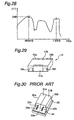
- Fig. 30 is a perspective view of a conventional coaxial filter comprising as shown dielectric coaxial resonators 30a and 30b, external electrodes 31a and 31b, inside circumferential electrodes 32a and 32b formed inside through-holes in the dielectric coaxial resonators 30a and 30b, connecting metal 33a and 33b, coupling substrate 34, and base 35.
- This coaxial filter device is described further below as thus comprising a first coaxial filter with a 950-MHz bandpass and a second coaxial filter with a 1.9-GHz bandpass.
- Figs. 31A and 31B are input and output Smith charts for the first and second coaxial filters, respectively, with impedance at 950 MHz indicated at point 22 and impedance at 1.9 GHz indicated at point 23.
- the characteristics of each single coaxial filter are such that the first coaxial filter has low impedance to the passband of the second coaxial filter and thus shorts, and the second coaxial filter has low impedance to the passband of the first coaxial filter and thus similarly shorts.
- a dual-band bandpass filter therefore cannot be produced by simply connecting two such coaxial filters together because the filters short at the passband of the other. Phase shifting is therefore required so that impedance to the passband of the other filter is high and an open state is maintained.
- Fig. 32 is a circuit diagram of a one-input, one-output dual-band bandpass filter using conventional coaxial filters. Shown in Fig. 32 are a first coaxial filter 36a and second coaxial filter 36b, and first and second phase shifters 37 and 38. The operation of this dual-band bandpass filter is described below.
- the impedance of the first coaxial filter 36a to the passband (1.9 GHz) of the second coaxial filter 36b is increased by the matched phase shifter 37.
- the impedance of the second coaxial filter 36b to the passband (950 MHz) of the first coaxial filter 36a is likewise increased by the matched phase shifter 38.
- the object of the present invention is to provide a compact, high performance, dual-band multilayer bandpass filter.
- the multilayer bandpass filter according to the present invention comprises a filter body of plural stacked ceramic sheets forming a first filter and a second filter in the filter body.
- a one-input, one-output filter can be achieved by providing a matching phase shift circuit for the first filter and the second filter.
- a one-input, two-output dividing filter can be further achieved by disposing a phase device only at the input side with two output terminals on the output side.
- a two-input, one-output combining filter can be achieved by disposing a phase device only at the output side with two input terminals on the input side.
- the number of components required to achieve a dual-band bandpass filter can thus be reduced, and a compact dual-band multilayer bandpass filter with stable, high performance can be achieved within the footprint of a single multilayer filter by providing a phase shift circuit.
- a dual-band multilayer bandpass filter includes a first filter arrangement F1 and a second filter arrangement F2.
- Each filter arrangement F1 or F2 includes a primary filter, or filter unit, 18 or 19 and a secondary filter 20a and 20b or 21a and 21b.
- the multilayer bandpass filter referred to herein includes only the primary filters, such as shown by a block 10 in Fig. 5A, and the dual-band multilayer bandpass filter referred to herein includes the multilayer bandpass filter and the secondary filters connected thereto.
- the first filter arrangement F1 as well as the first filter unit 18, has a 950-MHz bandpass
- the second filter arrangement F2 as well as the second filter unit 19, has a 1.9-GHz.
- the frequencies of these two filter arrangements are given only as examples.
- the first and second filter arrangements F1 and F2 may be arranged to pass frequencies other than 950 MHz and 1.9 GHz, respectively, as long as the signal passing through the first filter arrangement F1 has a frequency lower than that of the signal passing through the second filter arrangement F2.
- Fig. 1A is an exploded perspective view of a multilayer bandpass filter according to a first embodiment of the present invention.
- Fig. 1B is an equivalent circuit of the multilayer bandpass filter of Fig. 1A.
- Fig. 2 is a perspective view showing the outside of the multilayer bandpass filter after the layers are stacked together.
- Figs. 3 and 4 are Smith charts used to describe the phase characteristics of the first and second filters, respectively.
- the multilayer filter 10 comprises a first filter unit 18 formed in ceramic layers 11c and 11d, and second filter unit 19 formed in ceramic layers 11f and 11g.
- the layer 11c has a quarter-wave strip line resonator formed by electrodes 13a and 13a'. Electrodes 13a and 13a' are connected through a base electrode which is extended onto a front side surface of the layer 11c.
- the layer 11d has: an input electrode 15a; capacitance electrodes 9a and 9a' connected through a base electrode which is extended onto a back side surface (not shown) of the layer 11c; a coupling electrode 8 at about the center of the layer 11c; and an output electrode 15b.
- the input and output electrodes 15a and 15b are extended onto the back side surface.
- the input electrode 15a is capacitively coupled to electrode 13a through the ceramic layer 11c, as shown in Fig. 18.
- the electrode 13a is capacitively coupled to electrode 9a which is grounded.
- the electrode 13a is also capacitively coupled to the coupling electrode 8 which is in turn capacitively coupled to electrode 13a'.
- the electrode 13a' is capacitively coupled to electrode 9a' and also to output electrode 15b.
- the first filter unit 18 formed by layers 11c and 11d has an equivalent circuit as shown in Fig. 1B.
- the size of the electrodes 13a and 13a', as well as the size of other electrodes, are so selected to establish a bandpass filter for filtering 950 MHz.
- the layer 11f has a quarter-wave strip line resonator formed by electrodes 13b and 13b'.
- the electrodes 13b and 13b' are oriented in opposite direction to that of electrodes 13a and 13a'. Electrodes 13b and 13b' are connected through a base electrode which is extended onto a back side surface of the layer 11f.
- the layer 11g has: an input electrode 16a; capacitance electrodes 9b and 9b' connected through a base electrode which is extended onto the front side surface of the layer 11g; a coupling electrode 7 at about the center of the layer 11g; and an output electrode 16b.
- the input and output electrodes 16a and 16b are extended onto the front side surface.
- the second filter unit 19 formed by layers 11f and 11g has an equivalent circuit similar to that shown in Fig. 1B.
- the size of the electrodes 13b and 13b', as well as the size of other electrodes, are so selected to establish a bandpass filter for filtering 1.9 GHz.
- a ceramic layer 11e formed with a shield electrode 12b is provided between the layers 11d and 11f. Also a ceramic layer 11b formed with a shield electrode 12a is provided on top of layer 11c, and a ceramic layer 11h formed with a shield electrode 12c is provided under the layer 11g. Also a ceramic layer 11a is provided on top of layer 11b.
- These ceramic layers 11a to 11h have electrodes on one surface as explained above and are laminated together and co-fired to form a multilayer filter 10, as shown in Fig. 2.
- Front side surfaces of the multilayer filter 10 has ground electrode 17a in the center and input and output electrodes 16a and 16b on the opposite sides of the ground electrode 17a.
- the ground electrode 17a is connected to electrodes 12a, 13a, 13a', 12b, 9b, 9b' and 12c.
- back side surface of the multilayer filter 10 has ground electrode 17b in the center and input and output electrodes 15a and 15b on the opposite sides of the ground electrode 17b.
- the ground electrode 17b is connected to electrodes 12a, 9a, 9a', 12b, 13b, 13b' and 12c. Since the ground electrode 17a is provided between input and output electrodes 16a and 16b, the isolation between the input and output electrodes 16a and 16b is improved. The same can be said to the input and output electrodes 15a and 15b.
- a dual-band multilayer bandpass filter with a good attenuation characteristic can be achieved.
- input and output electrodes 16a and 16b can be provided only partially along the side surface. This is done for example by removing portions of the electrodes. As the removed part increases, the passband frequency increases. Thus, by adjusting the amount of portion to be removed, it is possible to precisely adjust the filtering frequency. If the electrode is removed more than enough, electrode may be added to decrease the passband frequency.
- Fig. 3 shows a Smith chart of the first filter unit 18 for filtering the signal of 950 MHz.
- the first filter unit shows about 50 ⁇ matching with respect to 950 MHz signal, and short-circuited with respect to 1.9 GHz.
- Fig. 4 shows a Smith chart of the second filter unit 19 for filter the signal of 1.9 GHz.
- the first filter unit shows about 50 ⁇ matching with respect to 1.9 GHz signal, and short-circuited with respect to 950 MHz.
- the impedance of the first multilayer filter unit is low at the passband (1.9 GHz) of the second multilayer filter unit, as shown in Fig. 3.
- the impedance of the second multilayer filter unit at the passband (950 MHz) of the first multilayer filter unit is low, as shown in Fig. 4.
- the first filter should make its impedance high at the passband of the second filter, and the second filter should make its impedance high at the passband of the first filter.
- a phase shift circuit comprising a lumped element is therefore disposed to the input/output terminals as shown in Fig. 5A.
- An inductor is thus connected to the input/output terminals of the first multilayer filter unit to increase impedance at the passband (1.9 GHz) of the second multilayer filter unit, and a capacitor is connected in series to the input/output terminals of the second multilayer filter unit to increase impedance at the passband (950 MHz) of the first multilayer filter unit.
- a filter with two bandpasses, at 950 MHz and 1.9 GHz, and good attenuation at other frequencies, is thus achieved as shown in Fig. 6.
- a further detail of the arrangement of Fig. 5A is described below.
- the dual-band multilayer bandpass filter employs the multilayer filter 10 shown in Fig. 1A.
- the multilayer filter 10 includes the first filter unit 18 and the second filter unit 19.
- the first filter unit 18, serving as the primary filter has its input 15a externally connected to a coil 20a, and its output 15b externally connected to a coil 20b.
- Coils 20a and 20b serve as the secondary filter which blocks signals in the range of 1.9 GHz, but passes signals in the range of 950 MHz.
- the second filter unit 19 also serving as the primary filter, has its input 16a externally connected to a capacitor 21a, and its output 16b externally connected to a capacitor 21b.
- Capacitors 21a and 21b serve as the secondary filter which blocks signals in the range of 950 MHz, but passes signals in the range of 1.9 GHz.
- the dual-band multilayer bandpass filter shown in Fig. 5A is a one-input one-output type.
- Fig. 6 shows the frequency characteristics of the dual-band multilayer bandpass filter of Fig. 5A.
- the filter of Fig. 5A has two filtering peak points 22 and 23 at frequencies 950 MHz and 1.9 GHz, respectively.
- Fig. 5B is a modification of the dual-band multilayer bandpass filter of Fig. 5A, and particularly shows a one-input two-output type, in which the outputs 15b and 16b are freed.
- Fig. 5C is another modification of the dual-band multilayer bandpass filter of Fig. 5A, and particularly shows a two-input one-output type, in which the inputs 15a and 16a are freed.
- Fig. 7A a modification of the multilayer bandpass filter 10 is shown.
- the filter of Fig. 7A has input electrode 15a connected directly to the electrode 13a, and output electrode 15b connected directly to the electrode 13a', as shown in Fig. 7B.
- Fig. 7B no capacitive coupling between the input electrode 15a and the electrode 13a is formed.
- Other arrangements are the same as that shown in Fig. 1A.
- Fig. 8 shows the assembled multilayer bandpass filter 10 of Fig. 7A.
- the input 15a to the first filter unit 18 in this modification is a power supply tap enabling more strong coupling with the resonator.
- the inputs 15a and 16a to the first and second filter units are provided on the left side of the multilayer filter 10, and the outputs 15b and 16b are provided on the right side.
- This filter also is connected with a phase shift circuit to establish a dual-band multilayer bandpass filter. Thus, the isolation between the input and output can be accomplished.
- FIG. 9 another modification of the multilayer bandpass filter 10 is shown.
- the multilayer filter 10 shown in Fig. 9 comprises a first filter unit 18 formed on the right half portion of ceramic layers 111c and 111d, and second filter unit 19 formed on the left half portion of ceramic layers 111c and 111d.
- the layer 111c has in its right half portion: an input electrode 115a; capacitance electrodes 109a and 109a' connected through a base electrode which is extended on the right side surface of the layer 111c; a coupling electrode 108; and an output electrode 115b.
- the input and output electrodes 115a and 115b are extended onto the front and back side surfaces, respectively.
- the layer 111c further has in its left half portion: an input electrode 116a; a coupling electrode 107; and an output electrode 116b.
- the input and output electrodes 116a and 116b are extended onto the front and back side surfaces, respectively.
- the layer 111d has in its right half portion a quarter-wave strip line resonator formed by electrodes 113a and 113a'. Electrodes 113a and 113a' are connected through a base electrode which is extended across the center of the layer 111d.
- the layer 111d further has in its left half portion a quarter-wave strip line resonator formed by electrodes 113b and 113b'. Electrodes 113b and 113b' are connected through a base electrode which is extended across the center of the layer 111d.
- Layers 111b and 111e with shield electrodes 112a and 112b, respectively, are provided on top and bottom of layers 111c and 111d, respectively.
- a top layer 111a is further provided.
- the centers of the layers 111b, 111c and 111d are formed with through-holes 124 for extending a conductive material therethrough.
- the ground electrodes are connected through the through-holes 124.
- through-holes 124 connect the top and bottom shield electrodes to the short-circuit terminals of the resonator to obtain a good ground and improve the isolation between the first and second filters.
- the multilayer bandpass filter shown in Fig 9 has the first and second filter resonators 18 and 19 on the same surface layers 111c and 111d.
- the gap between the shield layers is greater than when the two bandpasses filters are stacked.
- the Q factor of the resonator is thus higher, and a filter with less loss can be achieved.
- Fig. 10 shows the input and output locations of the multilayer bandpass filter of Fig. 9.
- a one-input and one-output, one-input and two-output, or a two-input and one-output configuration can also be achieved by forming the phase shift circuits as described above.
- a compact dual-band multilayer bandpass filter having one-input and one-output, one-input and two-outputs, or two-inputs and one-output by constructing a two-input, two-output dual-band multilayer bandpass filter comprising a first multilayer filter unit and a second multilayer filter unit in a multilayer filter comprising plural stacked ceramic sheets, and connecting a phase shift circuit thereto as described above.
- a second embodiment of the dual-band multilayer bandpass filter is shown.
- the difference is that ceramic layers 11i and 11j are further provided to form thereon the secondary filters.
- the quarter-wave strip line resonator formed by electrodes 13b and 13b' is oriented in opposite direction, i.e., in the same direction as the electrodes 13a and 13a'.
- Fig. 12 shows an equivalent circuit diagram of the dual-band multilayer bandpass filter shown in Fig. 11.
- the multilayer filter 10 comprises: ceramic sheets 11a to 11h; shield electrodes 12a, 12b, and 12c; quarter-wave strip line resonator electrodes 13a, 13a', 13b and 13b' with each resonator grounded at the same side; capacitance electrodes 9a, 9a', 9b and 9b'; input/output terminals 15a and 15b for the first multilayer filter unit; input/output terminals 16a and 16b for the second multilayer filter unit; transmission lines 25a and 25b; and capacitors 26a (formed between electrodes 7a and 16a) and 26b (formed between electrodes 7b and 16b) forming a phase shift circuit in the second multilayer filter unit.
- the transmission lines 25a and 25b serve as the secondary filters for the 950 MHz signals
- capacitors 26a and 26b serve as the secondary filters for the 1.9 GHz signals.
- the first multilayer filter unit comprises strip line resonator 13a and capacitance layer 14a disposed between shield electrodes 12a and 12b.
- a phase shift circuit for increasing the impedance of the first multilayer filter unit 18 in the passband (1.9 GHz) of the second multilayer filter unit is formed by the transmission lines 25a and 25b.
- the impedance of the second multilayer filter unit 19 to the passband (950 MHz) of the first multilayer filter unit is increased by the capacitors 26a and 26b.
- the layers 11a-11j are made of ceramic plate having the same dielectric constant. It is possible, however, to prepare layer 11i with a different ceramic plate having a dielectric constant lower than that in other layers.
- the second embodiment has been described as a one-input, one-output type dual-band multilayer bandpass filter, but other types, such as a one-input, two-output type can be alternatively achieved by disposing a phase shift circuit as described above on the input side only, and providing a first filter output terminal and a second filter output terminal on the output side.
- a two-input, one-output type can also be achieved by disposing a phase shift circuit as described above on the output side only with two terminals, one terminal for the first filter and one terminal for the second filter, provided on the input side.
- the resonators used in the dual-band multilayer bandpass filters described above are quarter-wave resonators grounded on one side, half-wave resonators and other types of resonators can be alternatively used.
- the dual-band multilayer bandpass filter of the invention has been described using only two resonators above, but three or more plural resonators can be used to the same effect.
- a third embodiment of the dual-band multilayer bandpass filter is shown.
- the second embodiment shown in Figs. 11 and 12 is one-input one-output type.
- the third embodiment shows one-input two-output type.
- the difference is that the transmission line 25b is eliminated, and the capacitance electrode 16b is eliminated.
- the third embodiment can be also used as a two-input one-output type, by using the electrodes 15b and 7b as inputs and electrode 15c as output.
- Figs. 15 and 16 a fourth embodiment of the dual-band multilayer bandpass filter is shown.
- the difference is that in Fig. 15 the electrodes 7a and 7b are eliminated.
- the capacitors for the secondary filters are obtained by the capacitance between electrodes 16a and 13b, and also between electrodes 16b and 13b'.
- Figs. 17 and 18 a fifth embodiment of the dual-band multilayer bandpass filter is shown.
- transmission lines 25a and 25b are provided in the separate ceramic layers. More specifically, the transmission line 25a is provided on a ceramic layer 11k above the first filter unit 18 and the transmission line 25b is provided on a ceramic layer 111 below the first filter unit 18.
- a sixth embodiment of the dual-band multilayer bandpass filter is shown.
- the difference is that in Fig. 19, a layer 11m with a shield electrode 12d is inserted between the layers 11i and 11c.
- the coupling between the electrodes on the layer 11i and the electrodes on the layer 11c can be prevented.
- Fig. 20 a seventh embodiment of the dual-band multilayer bandpass filter is shown.
- the layers 11i and 11j with the transmission lines 25a and 25b and electrodes 16a and 16b are eliminated, and instead, transmission lines 25a and 25b are provided on layer 11d extending from input and output electrodes 15a and 15b, and transmission lines 25c and 25d are provided on layer 11f extending from input and output electrodes 16a and 16b.
- Fig. 21 shows an equivalent circuit of the filter shown in Fig. 20.
- the secondary filters are all formed by transmission lines.
- the length of the transmission lines 25a and 25b is made shorter than that of the transmission lines 25c and 25d.
- the transmission lines 25a and 25b show high impedance with respect to 1.9 GHz, and low impedance with respect to 950 MHz.
- the transmission lines 25c and 25d show low impedance with respect to 1.9 GHz, and high impedance, or open, with respect to 950 MHz.
- FIG. 22 an eighth embodiment of the dual-band multilayer bandpass filter is shown.
- layers 11i and 11j with the transmission lines 25a and 25b and electrodes 16a and 16b are eliminated, and instead, open stubs 46a and 46b are provided on layer 11d branching from input and output electrodes 15a and 15b, and another open stubs 27a and 27b are provided on layer 11g branching from input and output electrodes 16a and 16b.
- Fig. 23 shows an equivalent circuit of the filter shown in Fig. 22.
- the secondary filters are all formed by open stubs.
- the length of the open stubs 46a and 46b is made shorter than that of the open stubs 27a and 27b.
- the open stubs 46a and 46b prevents the transmission of 1.9 GHz signal to the first filter unit 18, and the open stubs 27a and 27b prevents the transmission of 950 MHz signal to the second filter unit 19.
- the open stubs 46a and 46b can be formed in any other location or layer in the first filter unit 18, as long as the open stub branches from the electrode in the first filter unit 18.
- the open stubs 27a and 27b can be formed in any other location or layer in the second filter unit 19, as long as the open stub branches from the electrode in the second filter unit 19.
- a ninth embodiment of the dual-band multilayer bandpass filter is shown.
- This arrangement has one primary filter, which is filter unit 18, for filtering 950 MHz signal, and one secondary filter, defined by open stubs 29a and 29b, for filtering 1.9 GHz.
- this arrangement has layers 11a, 11b, 11n, 11c, 11d and 11e.
- the layers 11a, 11b, 11c, 11d and 11e are the same as those shown in Fig. 11.
- the layer 11n is inserted between layers 11b and 11c and is provided with open stubs 29a and 29b.
- the configuration and positioning of the open stubs 29a and 29b are so arranged that stubs 29a and 29b are electromagnetically coupled to filter the 1.9 GHz signal.
- Fig. 25 shows an equivalent circuit of the filter shown in Fig. 24.
- no secondary filter is provided for filtering the 950 MHz signal
- no primary filter is provided for filtering the 1.9 GHz signal.
- the open stubs 29a and 29b prevents the transmission of 950 MHz signal, and at the same time, the open stubs 29a and 29b are electromagnetically coupled to transmit 1.9 GHz signal.
- the distance between the shield electrodes 12a and 12b can be made relatively great, and the Q factor of the resonator is thus high, and a filter with less loss can be achieved.
- a tenth embodiment of the dual-band multilayer bandpass filter is shown.
- This arrangement has one primary filter, which is filter unit 19, for filtering 1.9 GHz signal, and one secondary filter, which is a notch filter defined by strip lines 28a, 28b and 28c, for filtering 950 MHz.
- the layer 11n with the stubs 29a and 29b is eliminated, and instead, layers 11p, 11q and 11r are inserted.
- Layer 11p has two parallel strip lines 28a and 28b.
- Layer 11q has one strip line 28c extended vertically to the strip lines 28a and 28b.
- Layer 11r has a shield electrode 12e.
- the configuration and positioning of the strip lines 28a, 28b and 28c are so arranged that signals having frequency higher than 950 MHz are cut off.
- Fig. 27 shows an equivalent circuit of the filter shown in Fig. 26, and Fig. 28 shows a characteristic graph.
Landscapes
- Physics & Mathematics (AREA)
- Electromagnetism (AREA)
- Control Of Motors That Do Not Use Commutators (AREA)
Claims (18)
- Mehrschichtbandpassfilter, enthaltend:dadurch gekennzeichnet, dass die ersten und die zweiten Eingabe- und Ausgabeelektroden (15a, 15b, 16a, 16b) getrennt voneinander vorgesehen sind und ihre jeweiligen Endabschnitte über die obere Oberfläche der aufeinanderliegenden Struktur gebogen sind.eine erste Filtereinheit (18), welche mehrere aufeinanderliegende Keramikschichten (11c, 11d), die einen Stripline-Resonator (13a, 13a) und eine Kopplungselektrode (9a, 9a', 8) aufweisen, besitzt,eine zweite Filtereinheit (19), die mehrere aufeinanderliegende Keramikschichten 11c, 11d), die einen Stripline-Resonator (13b, 13b') undeine Kopplungselektrode (9b, 9b', 7) aufweisen, besitzteine Abschirmelektrode (12b), die zwischen der ersten und der zweiten Filtereinheit (18, 19) eingefügt ist,wobei die zweite Filtereinheit (19) unter der ersten Filtereinheit (18) angeordnet ist, um eine aufeinanderliegende Struktur zu bilden,eine erste Eingabeelektrode (15a) für die Eingabe in die erste Filtereinheit (18), die auf einer außenliegenden Oberfläche der aufeinanderliegenden Struktur ausbildet ist und sich in Stapelrichtung erstreckt,eine erste Ausgabeelektrode (15b) für die Ausgabe der ersten Filtereinheit (18), die auf einer außenliegenden Oberfläche der aufeinanderliegenden Struktur ausgebildet ist und sich in Stapelrichtung erstreckt,eine zweite Eingabeelektrode (16a) für die Eingabe in die zweite Filtereinheit (19), die auf einer außenliegenden Oberfläche der aufeinanderliegenden Struktur ausgebildet ist und sich in Stapelrichtung erstreckt,eine zweite Ausgabeelektrode (16b) für die Ausgabe der zweiten Filtereinheit (19), die auf der außenliegenden Oberfläche der aufeinanderliegenden Struktur ausgebildet ist und sich in Stapelrichtung erstreckt,eine erste Erdungselektrode (17b), die auf der außenliegenden Oberfläche der aufeinanderliegenden Struktur ausgebildet ist und sich in Stapelrichtung erstreckt sowie zwischen der ersten Eingabeelektrode (15a) und der ersten Ausgabeelektrode (15b) angeordnet ist, undeine zweite Erdungselektrode (17a), die auf der außenliegenden Oberfläche der aufeinanderliegenden Struktur ausgebildet ist und sich in Stapelrichtung erstreckt sowie zwischen der zweiten Eingabeelektrode (16a) und der zweiten Ausgabeelektrode (16b) angeordnet ist,
- Mehrschichtbandpassfilter nach Anspruch 1,
bei dem sich die zweite Eingabeelektrode (16a) teilweise in die Stapelrichtung erstreckt. - Mehrschichtbandpassfilter nach Anspruch 1,
bei dem sich die zweite Ausgabeelektrode (16b) teilweise in die Stapelrichtung erstreckt. - Zweiband-Mehrschichtbandpassfilter enthaltend:dadurch gekennzeichnet, dasseine erste Filtereinheit (18) zum Filtern eines ersten Signals mit einer ersten Frequenz, wobei die erste Filtereinheit (18) mehrere aufeinanderliegende Keramikschichten (11c, 11d) mit einem Stripline-Resonator (13a, 13a') und einer Kopplungselektrode (9a, 9a', 8) enthält,eine zweite Filtereinheit (19) zum Filtern eines zweiten Signals mit einer zweiten Frequenz, die größer ist als die erste Frequenz, wobei die zweite Filtereinheit (19) mehrere aufeinanderliegende Keramikschichten (11f, 11g) mit einem Stripline-Resonator (13b, 13b') und einer Kopplungselektrode (9b, 9b', 7) enthält,eine Abschirmelektrode (12b), die zwischen der ersten und der zweiten Filtereinheit (18, 19) eingesetzt ist,wobei die zweite Filtereinheit (19) unter der ersten Filtereinheit (18) angeordnet ist, um eine aufeinanderliegende Struktur zu bilden,eine Eingabeelektrode (15a, 15c, 16a) für die Eingabe in die erste und die zweite Filtereinheit (18, 19), die auf einer außenliegenden Oberfläche der aufeinanderliegenden Struktur ausgebildet ist und sich in Stapelrichtung erstreckt,eine Ausgabeelektrode (15b, 15d, 16b) für die Ausgabe der ersten und zweiten Filtereinheit (18, 19), die auf der außenliegenden Oberfläche der aufeinanderliegenden Struktur ausgebildet ist und sich in Stapelrichtung erstreckt, undeine erste sowie eine zweite Erdungselektrode (17a, 17b), die auf der außenliegenden Oberfläche der aufeinanderliegenden Struktur ausgebildet sind und sich in Stapelrichtung erstrecken sowie zwischen der Eingabeelektrode (15a) und der Ausgabeelektrode (15b) angeordnet sind,ein erstes Sperrelement (25a, 25b; 25a', 25b'; 26a, 26b) mit der ersten Filtereinheit (18) verbunden ist, um das zweite Signal daran zu hindern, an die erste Filtereinheit (18) angelegt zu werden,ein zweites Sperrelement (26a, 26b; 25c, 25d; 27a, 27b) mit der zweiten Filtereinheit (19) verbunden ist, um das erste Signal daran zu hindern, an die zweite Filtereinheit (19) angelegt zu werden, unddie Eingabe- und Ausgabeelektroden getrennt voneinander vorgesehen sind und ihre Endabschnitte jeweils über die obere Oberfläche der aufeinanderliegenden Struktur gebogen sind.
- Zweiband-Mehrschichtbandpassfilter nach Anspruch 4,
bei dem das erste Sperrelement mit der Eingabeseite sowie der Ausgabeseite der ersten Filtereinheit (18) verbunden ist, bei dem das zweite Sperrelement mit der Eingabeseite sowie der Ausgabeseite der zweiten Filtereinheit (19) verbunden ist, bei dem das erste sowie das zweite Sperrelement an der Eingabeseite miteinander verbunden sind und bei dem das erste sowie das zweite Sperrelement an der Ausgabeseite miteinander verbunden sind, um einen Eine-Eingabe-/Eine-Ausgabe-Zweitband-Mehrschichtbandpassfilter zu bilden. - Zweiband-Mehrschichtbandpassfilter nach Anspruch 4,
bei dem das erste Sperrelement mit der Eingabeseite der ersten Filtereinheit (18) verbunden ist, bei dem das zweite Sperrelement mit der Eingabeseite der zweiten Filtereinheit verbunden ist und bei dem das erste sowie das zweite Sperrelement an der Eingabeseite miteinander verbunden sind, um ein Eine-Eingabe-/Zwei-Ausgaben-Zweiband-Mehrschichtbandpassfilter zu bilden. - Zweiband-Mehrschichtbandpassfilter nach Anspruch 4,bei dem das erste Sperrelement mit einer Ausgabeseite der ersten Filtereinheit (18) verbunden ist, bei dem das zweite Sperrelement mit einer Ausgabeseite der zweiten Filtereinheit (19) verbunden ist undbei dem das erste sowie das zweite Sperrelement an der Ausgabeseite miteinander verbunden sind, um einen Zwei-Eingaben-/Eine-Ausgabe-Zweiband-Mehrschichtbandpassfilter zu bilden.
- Zweiband-Mehrschichtbandpassfilter nach Anspruch 4,
bei dem das erste Sperrelement eine Induktionsspule (20a, 20b) ist, welche extern mit der ersten Filtereinheit (18) verbunden ist. - Zweiband-Mehrschichtbandpassfilter nach Anspruch 4,
bei dem das zweite Sperrelement ein Kondensator (21a, 21b) ist, der mit der zweiten Filtereinheit (19) extern verbunden ist. - Zweiband-Mehrschichtbandpassfilter nach Anspruch 4,
bei dem das erste Sperrelement eine Stripline-Drosselspule (25a, 25b; 25a', 25b') ist, die auf einer Keramikschicht in der aufeinanderliegenden Struktur ausgebildet ist. - Zweiband-Mehrschichtbandpassfilter nach Anspruch 10,
bei dem die Keramikschicht mit der Stripline-Drosselspule eine Dielektrizitätskonstante aufweist, welche sich von der der anderen Keramikschichten unterscheidet. - Zweiband-Mehrschichtbandpassfilter nach Anspruch 4,
bei dem das zweite Sperrelement ein Kondensator (26a, 26b) ist, der durch ein Paar Elektroden gebildet ist, welche auf Keramikschichten in der aufeinanderliegenden Struktur ausgebildet sind. - Zweiband-Mehrschichtbandpassfilter nach Anspruch 4,
bei dem das zweite Sperrelement eine Stripline-Drosselspule (25c, 25d) ist, die auf einer Keramikschicht in der aufeinanderliegenden Struktur ausgebildet ist. - Zweiband-Mehrschichtbandpassfilter nach Anspruch 4,
bei dem das erste Sperrelement ein offener Stub (46a, 46b) ist, der auf einer Keramikschicht in der aufeinanderliegenden Struktur ausgebildet ist. - Zweiband-Mehrschichtbandpassfilter nach Anspruch 4,
bei dem das zweite Sperrelement ein offener Stub (27a, 27b) ist, der auf einer Keramikschicht in der aufeinanderliegenden Struktur ausgebildet ist. - Zweiband-Mehrschichtbandpassfilter nach Anspruch 4,
bei dem die aufeinanderliegende Struktur als Ganzes gebrannt ist. - Zweiband-Mehrschichtbandpassfilter, enthaltend:dadurch gekennzeichnet, dasseine erste Filtereinheit (18), um ein erstes Signal mit einer ersten Frequenz zu filtern, wobei die erste Filtereinheit (18) mehrere aufeinanderliegende Keramikschichten (11c, 11d) enthält, die einen Stripline-Resonator (13a, 13a') sowie eine Kopplungselektrode aufweisen,eine zweite Filtereinheit (29a, 29b; 28a, 28b, 28c) zum Filtern eines zweiten Signals mit einer zweiten Frequenz, die größer ist als die erste Frequenz, wobei die zweite Filtereinheit mehrere aufeinanderliegende Keramikschichten mit offenen Stubs (29a, 29b; 28a, 28b) enthält,wobei die zweite Filtereinheit (29a, 29b 28a, 28b) unter der ersten Filtereinheit (18) angeordnet ist, um eine aufeinanderliegende Struktur zu bilden,eine Eingabeelektrode (16a) für die Eingabe in die erste Filtereinheit (18) und die zweite Filtereinheit (29a, 29b; 28a, 28b), die auf einer außenliegenden Oberfläche der aufeinanderliegenden Struktur ausgebildet ist und sich in Stapelrichtung erstreckt, undeine Ausgabeelektrode (16b) für die Ausgabe der ersten Filtereinheit (18) und der zweiten Filtereinheit (29a, 29b; 28a, 28b), die auf der außenliegenden Oberfläche der aufeinanderliegenden Struktur ausgebildet ist und sich in Stapelrichtung erstreckt,
die Eingabe- und Ausgabeelektroden (16a, 16b) getrennt voneinander vorgesehen sind und jeder ihrer Endabschnitte über die obere Oberfläche der aufeinanderliegenden Struktur gebogen ist. - Zweiband-Mehrschichtbandpassfilter nach Anspruch 17,
bei dem die zweite Filtereinheit (28a, 28b, 28c) mehrere aufeinanderliegende Keramikschichten (11p, 11q) mit einer zusätzlichen Stripline (28c) enthält.
Applications Claiming Priority (4)
| Application Number | Priority Date | Filing Date | Title |
|---|---|---|---|
| JP20161496 | 1996-07-31 | ||
| JP20161496 | 1996-07-31 | ||
| JP201614/96 | 1996-07-31 | ||
| PCT/JP1997/002660 WO1998005120A1 (en) | 1996-07-31 | 1997-07-31 | Dual-band multilayer bandpass filter |
Publications (2)
| Publication Number | Publication Date |
|---|---|
| EP0916185A1 EP0916185A1 (de) | 1999-05-19 |
| EP0916185B1 true EP0916185B1 (de) | 2001-11-07 |
Family
ID=16443987
Family Applications (1)
| Application Number | Title | Priority Date | Filing Date |
|---|---|---|---|
| EP97933859A Expired - Lifetime EP0916185B1 (de) | 1996-07-31 | 1997-07-31 | Mehrschichtiger zweiband-bandpassfilter |
Country Status (5)
| Country | Link |
|---|---|
| US (1) | US6147571A (de) |
| EP (1) | EP0916185B1 (de) |
| JP (1) | JP2000516060A (de) |
| DE (1) | DE69708104T2 (de) |
| WO (1) | WO1998005120A1 (de) |
Cited By (1)
| Publication number | Priority date | Publication date | Assignee | Title |
|---|---|---|---|---|
| DE102005046445B4 (de) | 2005-09-28 | 2019-10-10 | Snaptrack, Inc. | Bandpassfilter |
Families Citing this family (47)
| Publication number | Priority date | Publication date | Assignee | Title |
|---|---|---|---|---|
| JPH11136002A (ja) * | 1997-10-30 | 1999-05-21 | Philips Japan Ltd | 誘電体フィルタ及び誘電体フィルタの通過帯域特性を調整する方法 |
| JPH11346104A (ja) | 1998-05-29 | 1999-12-14 | Philips Japan Ltd | 誘電体フィルタ |
| EP1650865B1 (de) * | 1998-10-27 | 2009-10-21 | Murata Manufacturing Co., Ltd. | Zusammengestellte Hochfrequenzkomponente und damit ausgerüstetes mobiles Kommunikationsgerät |
| JP2000323901A (ja) * | 1999-05-07 | 2000-11-24 | Murata Mfg Co Ltd | 積層型lcフィルタ |
| US6625470B1 (en) * | 2000-03-02 | 2003-09-23 | Motorola, Inc. | Transmitter |
| JP3478264B2 (ja) * | 2000-03-10 | 2003-12-15 | 株式会社村田製作所 | 弾性表面波装置 |
| JP3707351B2 (ja) * | 2000-03-31 | 2005-10-19 | 株式会社村田製作所 | 高周波モジュール及びそれを用いた無線機器 |
| DE60226111T2 (de) * | 2001-03-02 | 2009-05-28 | Panasonic Corp., Kadoma | Dielektrisches filter und antennenweiche |
| US6501353B2 (en) * | 2001-03-16 | 2002-12-31 | Illinois Superconductor Corporation | Duplexed front-end for a radio transceiver system |
| US7023301B2 (en) * | 2001-05-16 | 2006-04-04 | Matsushita Electric Industrial Co., Ltd. | Laminated filter with a single shield conductor, integrated device, and communication apparatus |
| TW486861B (en) * | 2001-07-04 | 2002-05-11 | Ind Tech Res Inst | Impedance matching circuit for a multi-band power amplifier |
| JP2003051729A (ja) * | 2001-08-06 | 2003-02-21 | Tdk Corp | 積層型フィルタアレイ |
| US6847282B2 (en) * | 2001-10-19 | 2005-01-25 | Broadcom Corporation | Multiple layer inductor and method of making the same |
| TW519749B (en) * | 2002-01-23 | 2003-02-01 | United Microelectronics Corp | Gateless diode device of ESD protection circuit and its manufacturing method |
| JP3932962B2 (ja) * | 2002-04-17 | 2007-06-20 | 株式会社村田製作所 | バンドパスフィルタ及び通信機 |
| KR100430253B1 (ko) * | 2002-05-10 | 2004-05-03 | 엘지이노텍 주식회사 | 스트립 라인을 이용한 필터회로 제조방법 |
| US6982609B1 (en) * | 2002-05-15 | 2006-01-03 | Zeevo | System method and apparatus for a three-line balun with power amplifier bias |
| US7283793B1 (en) * | 2002-05-15 | 2007-10-16 | Broadcom Corporation | Package filter and combiner network |
| FI20021328A0 (fi) * | 2002-07-05 | 2002-07-05 | Nokia Corp | Monikerrossuodatin |
| TWI239116B (en) * | 2004-09-01 | 2005-09-01 | Ind Tech Res Inst | Dual-band bandpass filter |
| US7680477B2 (en) * | 2004-09-03 | 2010-03-16 | Texas Instruments Incorporated | Integrated radio frequency filters for multiband transceivers |
| KR20060111850A (ko) * | 2005-04-25 | 2006-10-30 | 쿄세라 코포레이션 | 밴드패스 필터, 고주파 모듈 및 무선통신기기 |
| US7755457B2 (en) * | 2006-02-07 | 2010-07-13 | Harris Corporation | Stacked stripline circuits |
| US7468642B2 (en) | 2006-12-12 | 2008-12-23 | International Business Machines Corporation | Multi band pass filters |
| JP4758942B2 (ja) * | 2007-05-10 | 2011-08-31 | 株式会社エヌ・ティ・ティ・ドコモ | デュアルバンド共振器およびデュアルバンドフィルタ |
| DE102007024895B4 (de) * | 2007-05-29 | 2015-08-27 | Epcos Ag | Multiband-Filter |
| JP4483904B2 (ja) * | 2007-07-30 | 2010-06-16 | Tdk株式会社 | 貫通型積層コンデンサ |
| WO2009028691A1 (ja) * | 2007-08-29 | 2009-03-05 | Kyocera Corporation | バンドパスフィルタならびにそれを用いた無線通信モジュールおよび無線通信機器 |
| US8138852B2 (en) * | 2007-10-31 | 2012-03-20 | Ntt Docomo, Inc. | Duplexer and transceiver |
| JP5288885B2 (ja) * | 2008-05-28 | 2013-09-11 | 京セラ株式会社 | バンドパスフィルタならびにそれを用いた無線通信モジュールおよび無線通信機器 |
| JP5288904B2 (ja) * | 2008-06-26 | 2013-09-11 | 京セラ株式会社 | バンドパスフィルタならびにそれを用いた無線通信モジュールおよび無線通信機器 |
| US8704619B2 (en) | 2008-05-28 | 2014-04-22 | Kyocera Corporation | Bandpass filter and radio communication module and radio communication device using the same |
| JP5224908B2 (ja) * | 2008-05-28 | 2013-07-03 | 京セラ株式会社 | バンドパスフィルタならびにそれを用いた無線通信モジュールおよび無線通信機器 |
| JP5288903B2 (ja) * | 2008-06-26 | 2013-09-11 | 京セラ株式会社 | バンドパスフィルタならびにそれを用いた無線通信モジュールおよび無線通信機器 |
| US8710942B2 (en) | 2008-05-28 | 2014-04-29 | Kyocera Corporation | Bandpass filter and radio communication module and radio communication device using the same |
| JP5464864B2 (ja) * | 2009-02-25 | 2014-04-09 | 京セラ株式会社 | フィルタ回路ならびにそれを用いた無線通信モジュールおよび無線通信機器 |
| WO2011099439A1 (ja) * | 2010-02-09 | 2011-08-18 | マークデバイシス株式会社 | 反共振周波数可変型複合共振回路 |
| US8169277B2 (en) * | 2010-02-19 | 2012-05-01 | Harris Corporation | Radio frequency directional coupler device and related methods |
| WO2011147470A1 (en) * | 2010-05-28 | 2011-12-01 | Verigy (Singapore) Pte. Ltd. | Electrical double filter structure and its multi -layer implementation |
| KR102047812B1 (ko) * | 2013-05-02 | 2019-11-22 | 삼성전자주식회사 | 다중 대역 안테나 장치 및 다중 대역 안테나를 포함하는 무선 통신 장치 |
| JP6545398B2 (ja) | 2016-11-08 | 2019-07-17 | 三菱電機株式会社 | マルチバンドフィルタ |
| US10778261B2 (en) | 2017-06-14 | 2020-09-15 | Harris Corporation | Electronic device including radio frequency (RF) filter module with stacked coaxial resonators and related methods |
| RU2715358C1 (ru) * | 2019-05-23 | 2020-02-26 | Федеральное государственное автономное образовательное учреждение высшего образования "Сибирский федеральный университет" | Высокоселективный полосковый фильтр верхних частот |
| CN218959175U (zh) * | 2020-05-07 | 2023-05-02 | 株式会社村田制作所 | 多层基板模块 |
| JP2023125379A (ja) | 2022-02-28 | 2023-09-07 | Tdk株式会社 | 積層型電子部品 |
| WO2023240330A1 (en) * | 2022-06-14 | 2023-12-21 | Huawei Technologies Canada Co., Ltd. | Dual-band impedance matching circuit and method of impedance matching |
| CN115295985B (zh) * | 2022-07-18 | 2023-05-23 | 华南理工大学 | 一种适用于双频段通信系统的双通带带通滤波器及系统 |
Family Cites Families (9)
| Publication number | Priority date | Publication date | Assignee | Title |
|---|---|---|---|---|
| US5184096A (en) * | 1989-05-02 | 1993-02-02 | Murata Manufacturing Co., Ltd. | Parallel connection multi-stage band-pass filter comprising resonators with impedance matching means capacitively coupled to input and output terminals |
| DE4203960C2 (de) * | 1991-02-15 | 1995-05-24 | Murata Manufacturing Co | Bandpaßfilter |
| JP2502824B2 (ja) * | 1991-03-13 | 1996-05-29 | 松下電器産業株式会社 | 平面型誘電体フィルタ |
| JPH04299815A (ja) * | 1991-03-28 | 1992-10-23 | Murata Mfg Co Ltd | 複合電子部品 |
| US5291161A (en) * | 1991-07-22 | 1994-03-01 | Matsushita Electric Industrial Co., Ltd. | Microwave band-pass filter having frequency characteristic of insertion loss steeply increasing on one outside of pass-band |
| JPH0555809A (ja) * | 1991-08-27 | 1993-03-05 | Murata Mfg Co Ltd | フイルタ回路 |
| JP3201005B2 (ja) * | 1992-08-31 | 2001-08-20 | 株式会社村田製作所 | デュプレクサ |
| DE69432060T2 (de) * | 1993-08-24 | 2003-11-20 | Matsushita Electric Industrial Co., Ltd. | Geschichtete dielektrische Antennenweiche |
| JP3139327B2 (ja) * | 1995-05-31 | 2001-02-26 | 株式会社村田製作所 | 高周波複合部品 |
-
1997
- 1997-07-31 JP JP10508707A patent/JP2000516060A/ja not_active Withdrawn
- 1997-07-31 WO PCT/JP1997/002660 patent/WO1998005120A1/en not_active Ceased
- 1997-07-31 EP EP97933859A patent/EP0916185B1/de not_active Expired - Lifetime
- 1997-07-31 US US09/147,562 patent/US6147571A/en not_active Expired - Lifetime
- 1997-07-31 DE DE69708104T patent/DE69708104T2/de not_active Expired - Fee Related
Cited By (1)
| Publication number | Priority date | Publication date | Assignee | Title |
|---|---|---|---|---|
| DE102005046445B4 (de) | 2005-09-28 | 2019-10-10 | Snaptrack, Inc. | Bandpassfilter |
Also Published As
| Publication number | Publication date |
|---|---|
| US6147571A (en) | 2000-11-14 |
| EP0916185A1 (de) | 1999-05-19 |
| JP2000516060A (ja) | 2000-11-28 |
| DE69708104D1 (de) | 2001-12-13 |
| DE69708104T2 (de) | 2002-07-11 |
| WO1998005120A1 (en) | 1998-02-05 |
Similar Documents
| Publication | Publication Date | Title |
|---|---|---|
| EP0916185B1 (de) | Mehrschichtiger zweiband-bandpassfilter | |
| EP1742354B1 (de) | Mehrlagiges Bandpassfilter | |
| US4879533A (en) | Surface mount filter with integral transmission line connection | |
| US5023866A (en) | Duplexer filter having harmonic rejection to control flyback | |
| US6191666B1 (en) | Miniaturized multi-layer ceramic lowpass filter | |
| US5357227A (en) | Laminated high-frequency low-pass filter | |
| US4963843A (en) | Stripline filter with combline resonators | |
| US6696903B1 (en) | Laminated dielectric filter, and antenna duplexer and communication equipment using the same | |
| JP3458720B2 (ja) | フィルタ装置、デュプレクサ及び通信機装置 | |
| US6359531B1 (en) | Multilayer filter with electrode patterns connected on different side surfaces to side electrodes and input/output electrodes | |
| US6522220B2 (en) | Frequency variable filter, antenna duplexer, and communication apparatus incorporating the same | |
| US6608533B2 (en) | Matching circuit chip, filter with matching circuit, duplexer and cellular phone | |
| US20030043759A1 (en) | LC filter circuit, laminated LC composite component, multiplexer, and radio communication device | |
| JPH0372701A (ja) | 並列多段型帯域通過フィルタ | |
| US6492886B1 (en) | Laminated filter, duplexer, and mobile communication apparatus using the same | |
| JPH10290108A (ja) | 方向性結合器 | |
| US6097268A (en) | Multilayer duplexer with no shielding electrodes | |
| EP0993063A2 (de) | Duplexer und Kommunikationsvorrichtung | |
| US6121854A (en) | Reduced size 2-way RF power divider incorporating a low pass filter structure | |
| US6504452B2 (en) | Low-pass filter and mobile communication device using the same | |
| US6369668B1 (en) | Duplexer and communication apparatus including the same | |
| US12451583B2 (en) | Power splitter and communication apparatus | |
| JP2666092B2 (ja) | 誘電体フィルタ | |
| RU2060571C1 (ru) | Частотный разделитель на коаксиальных диэлектрических резонаторах | |
| JP3368386B2 (ja) | 誘電体フィルタ |
Legal Events
| Date | Code | Title | Description |
|---|---|---|---|
| PUAI | Public reference made under article 153(3) epc to a published international application that has entered the european phase |
Free format text: ORIGINAL CODE: 0009012 |
|
| 17P | Request for examination filed |
Effective date: 19990301 |
|
| AK | Designated contracting states |
Kind code of ref document: A1 Designated state(s): DE FR GB |
|
| 17Q | First examination report despatched |
Effective date: 19990812 |
|
| GRAG | Despatch of communication of intention to grant |
Free format text: ORIGINAL CODE: EPIDOS AGRA |
|
| GRAG | Despatch of communication of intention to grant |
Free format text: ORIGINAL CODE: EPIDOS AGRA |
|
| GRAG | Despatch of communication of intention to grant |
Free format text: ORIGINAL CODE: EPIDOS AGRA |
|
| GRAG | Despatch of communication of intention to grant |
Free format text: ORIGINAL CODE: EPIDOS AGRA |
|
| GRAG | Despatch of communication of intention to grant |
Free format text: ORIGINAL CODE: EPIDOS AGRA |
|
| GRAH | Despatch of communication of intention to grant a patent |
Free format text: ORIGINAL CODE: EPIDOS IGRA |
|
| GRAH | Despatch of communication of intention to grant a patent |
Free format text: ORIGINAL CODE: EPIDOS IGRA |
|
| GRAA | (expected) grant |
Free format text: ORIGINAL CODE: 0009210 |
|
| AK | Designated contracting states |
Kind code of ref document: B1 Designated state(s): DE FR GB |
|
| REF | Corresponds to: |
Ref document number: 69708104 Country of ref document: DE Date of ref document: 20011213 |
|
| REG | Reference to a national code |
Ref country code: GB Ref legal event code: IF02 |
|
| PLBE | No opposition filed within time limit |
Free format text: ORIGINAL CODE: 0009261 |
|
| STAA | Information on the status of an ep patent application or granted ep patent |
Free format text: STATUS: NO OPPOSITION FILED WITHIN TIME LIMIT |
|
| 26N | No opposition filed | ||
| PGFP | Annual fee paid to national office [announced via postgrant information from national office to epo] |
Ref country code: FR Payment date: 20090710 Year of fee payment: 13 |
|
| PGFP | Annual fee paid to national office [announced via postgrant information from national office to epo] |
Ref country code: GB Payment date: 20090729 Year of fee payment: 13 Ref country code: DE Payment date: 20090723 Year of fee payment: 13 |
|
| GBPC | Gb: european patent ceased through non-payment of renewal fee |
Effective date: 20100731 |
|
| REG | Reference to a national code |
Ref country code: FR Ref legal event code: ST Effective date: 20110331 |
|
| PG25 | Lapsed in a contracting state [announced via postgrant information from national office to epo] |
Ref country code: DE Free format text: LAPSE BECAUSE OF NON-PAYMENT OF DUE FEES Effective date: 20110201 |
|
| REG | Reference to a national code |
Ref country code: DE Ref legal event code: R119 Ref document number: 69708104 Country of ref document: DE Effective date: 20110201 |
|
| PG25 | Lapsed in a contracting state [announced via postgrant information from national office to epo] |
Ref country code: FR Free format text: LAPSE BECAUSE OF NON-PAYMENT OF DUE FEES Effective date: 20100802 |
|
| PG25 | Lapsed in a contracting state [announced via postgrant information from national office to epo] |
Ref country code: GB Free format text: LAPSE BECAUSE OF NON-PAYMENT OF DUE FEES Effective date: 20100731 |