EP0917048B1 - Adressengenerator und Verfahren zur indirekten Adressierung in einem einzigen Zyklus - Google Patents
Adressengenerator und Verfahren zur indirekten Adressierung in einem einzigen Zyklus Download PDFInfo
- Publication number
- EP0917048B1 EP0917048B1 EP98119388A EP98119388A EP0917048B1 EP 0917048 B1 EP0917048 B1 EP 0917048B1 EP 98119388 A EP98119388 A EP 98119388A EP 98119388 A EP98119388 A EP 98119388A EP 0917048 B1 EP0917048 B1 EP 0917048B1
- Authority
- EP
- European Patent Office
- Prior art keywords
- address
- indirect addressing
- data pointer
- addressing mode
- register
- Prior art date
- Legal status (The legal status is an assumption and is not a legal conclusion. Google has not performed a legal analysis and makes no representation as to the accuracy of the status listed.)
- Expired - Lifetime
Links
Images
Classifications
-
- G—PHYSICS
- G06—COMPUTING OR CALCULATING; COUNTING
- G06F—ELECTRIC DIGITAL DATA PROCESSING
- G06F12/00—Accessing, addressing or allocating within memory systems or architectures
- G06F12/02—Addressing or allocation; Relocation
-
- G—PHYSICS
- G06—COMPUTING OR CALCULATING; COUNTING
- G06F—ELECTRIC DIGITAL DATA PROCESSING
- G06F9/00—Arrangements for program control, e.g. control units
- G06F9/06—Arrangements for program control, e.g. control units using stored programs, i.e. using an internal store of processing equipment to receive or retain programs
- G06F9/30—Arrangements for executing machine instructions, e.g. instruction decode
- G06F9/34—Addressing or accessing the instruction operand or the result ; Formation of operand address; Addressing modes
- G06F9/35—Indirect addressing
Definitions
- This invention relates generally to pointers and, more specifically, to a data pointer for generating an indirect addressing mode address within a single cycle for a selected one of a plurality of multiple indirect addressing modes.
- processor is an entity where a central processing unit (CPU) is present and is used to fetch and execute stored instructions or microcode.
- CPU central processing unit
- processors are microcontrollers, microprocessors, and digital signal processors.
- Each type of processor operates on data which is commonly referred to as operands. This data is generally stored in registers or memory space.
- An instruction directs the CPU of a processor to execute a certain-operation as well as to identify one or more operand(s) for the operation.
- Processors offer various means for addressing the data for an operation. These means are commonly referred to as addressing modes.
- the addressing modes are typically used for arithmetic and logical operations and data move operations and may apply to a source operand, a destination operand, or both.
- the data pointer must be able to generate the indirect addressing mode address within a single cycle for the selected indirect addressing mode.
- the data pointer must be able to generate the indirect addressing mode address within a single cycle for the selected indirect addressing mode.
- the data pointer must be able to generate the indirect addressing mode address within a single cycle for the selected indirect addressing mode without significantly increasing the amount of silicon real estate in the processor architecture.
- U.S. 4,616,313 discloses an address calculation circuit for a pipeline control-system data processing apparatus.
- the described circuit is rather complex in its structure and therefore needs a high amount of silicon real estate in the processor architecture.
- a data pointer for generating an indirect addressing mode address within a single cycle for a selected one of a plurality of multiple indirect addressing modes.
- the data pointer is to be used with a processor architecture scheme which allows for encoding of multiple addressing modes.
- a data pointer register is coupled to the processor architecture scheme and is used for storing a current address of an operand to be used in a simple indirect addressing mode.
- An incrementer is coupled to the data pointer register for incrementing the current address of the operand to be used in a simple indirect data addressing mode by a set number for generating an address of an operand to be used in an indirect addressing mode with auto preincrement.
- An adder is coupled to the data pointer register for combining the current address of an operand to be used in a simple indirect data addressing mode with an offset number for generating an address of an operand to be used in an indirect addressing mode with offset.
- a multiplexer circuit is coupled to an output of the data pointer register, to an output of the incrementer, and to an output of the adder. The multiplexer is used for selecting a desired indirect addressing mode address.
- a method for providing a data pointer for generating an indirect addressing mode address within a single cycle for a selected one of a plurality of multiple indirect addressing modes comprising the steps of: providing a processor architecture scheme which allows for encoding of multiple addressing modes; providing a data pointer register coupled to the processor architecture scheme for storing a current address of an operand to be used in a simple indirect addressing mode; providing an incrementer coupled to the data pointer register for incrementing the current address of an operand to be used in a simple indirect data addressing mode by a set number for generating an address of an operand to be used in an indirect addressing mode with auto preincrement; providing an adder coupled to the data pointer register for combining the current address of an operand to be used in a simple indirect data addressing mode with an offset number for generating an address of an operand to be used in an indirect addressing mode with offset; and providing a multiplexer circuit coupled to an output of the data pointer register, to an output of
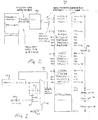
- a data pointer 10 for generating an indirect addressing mode address within a single cycle for a selected one of a plurality of multiple indirect addressing modes is shown.
- the data pointer 10 is to be implemented in a processor architecture scheme 30 ( Figure 2) which allows for the encoding of multiple indirect addressing modes.
- the data pointer 10 has a data pointer register 12 which is coupled to the processor architecture scheme 30.
- the data pointer register 12 is used for storing a current address of an operand to be used in a simple indirect addressing mode.
- the data pointer 10 has an incrementer 14 which has an input coupled to an output of the data pointer register 12.
- the incrementer 14 is used for incrementing the current address of the operand stored in the data pointer register 12 (i.e., current address of the operand to be used in a simple indirect addressing mode).
- the incrementer 14 increases this address by a set number.
- the incrementer 14 increments the current address stored in the data pointer register 12 by one address location.
- the data pointer 10 further has an adder 16 which has an input coupled to an output of the data pointer register 12.
- the adder 16 is used for combining the current address stored in the data pointer register 12 with an offset value. By combining the current address in the data pointer register 12 with an offset value, the adder 16 is able to generate the address of an operand to be used in an indirect addressing mode with offset.
- the offset value may be loaded from any memory device in the system. In the preferred embodiment of the present invention the offset value is stored in an offset register 20 which is stored in the data memory 32 ( Figure 2) of the processor architecture 30 ( Figure 2).
- the adder 16 may be any type of adder.
- the adder 16 may be a look ahead adder but this will require the use of additional silicon real estate which is not desired. Preferably, a simple serial adder with a serial carry is used.
- a multiplexer circuit 18 has a first input coupled to an output of the data pointer register 12, a second input coupled to an output of the incrementer 14, and a third input coupled to an output of the adder 16.
- the multiplexer circuit 18 is used for selecting a desired indirect addressing mode address generated by the aforementioned elements and outputting the selected address to an instruction register.
- a selection line 22 is coupled to the multiplexer circuit 18.
- the selection line 22 is further coupled to the processor architecture scheme 30. When a desired indirect addressing mode is selected in the processor architecture scheme 30, the selection line 22 will signal the multiplexer circuit 18 which address to output to the instruction register.
- the processor architecture scheme 30 must allow for the encoding of multiple addressing modes.
- the processor architecture scheme 30 will allow for the encoding of multiple indirect addressing modes through the use of virtual register addresses. This allows the processor architecture scheme 30 to maximize the number of directly addressable registers.
- the data pointer register 12 is implemented in data memory 32.
- the data memory 32 is comprised of a plurality of address locations 34.
- the data memory 32 is a linearized 4K memory which is divided into a plurality of banks 36 wherein each bank 36 has 256 address locations 34.
- the data pointer register 12 has one or more virtual register address locations 38 reserved in the register address map. Each reserved virtual register address location 38 will initiate an indirect addressing mode when accessed.
- Indirect addressing with auto increment or auto decrement are forms of indirect addressing where the data pointer register 12 is incremented or decremented either before the data access (i.e., pre-increment or pre-decrement) or after the data access (i.e., post-increment or post-decrement).
- the address of the operand is calculated by adding an offset value to the contents of the data pointer register 12.
- the offset value may be embedded in the instruction or may come from yet another register.
- the offset value comes from the "w" register 20 ( Figure 1), which is the accumulator or "working" register.
- the data pointer register 12 may be incremented or decremented before or after the operand access.
- the data pointer register 12 will require a separate virtual register address location 38 in data memory 32 for each indirect addressing mode to be implemented. In the preferred embodiment of the present invention, five virtual register address locations 38 are required to implement the five indirect addressing modes discussed above. However, additional or fewer indirect addressing modes may be implemented depending on the use of the data pointer register 12. Furthermore, additional data pointer registers 12 may be implemented in data memory 32. Each data pointer register 12 will have one or more virtual register address locations 38 reserved in the register address map. Each reserved virtual register address location 38 will initiate an indirect addressing mode for the associated data pointer register 12 when accessed. Each data pointer register 12 is a readable and writable address location.
- each data pointer register 12 is a 12 bit wide pointer capable of accessing a 4K byte long memory area. Therefore, each data pointer register 12 is organized as two 8 bit wide registers (high byte and low byte) which are accessible as readable and writable registers. Thus, in the preferred embodiment of the present invention, 7 address locations are used to implement a 12 bit wide data pointer with five indirect addressing modes.
- the first 128 locations are reserved for special function registers. These locations are also where the special indirect addresses are located.
- One or more data pointer registers 12 will also be located in this area.
- Each data pointer register 12 will have one or more virtual register address locations 38 reserved in the register address map to initiate indirect addressing. If none of the indirect addressing locations are accessed, direct addressing will occur. If an instruction accesses one of the reserved address locations 38, an indirect addressing mode is to be used with the associated data pointer register 12. For example, if the instruction is "ADD w,12h", the instruction will normally add the contents of "w” with the contents in address 12h and place the answer in- "w”.
- address 12h is a reserved address location for the data pointer register 12 at addresses 10h, 11h .
- "w" will be added to the contents of the real location pointed to by the data pointer register 36 at addresses 10h, 11h. The total will then be stored in "w”.
- Address 12h also states that a post increment is involved. Thus, the data pointer register 36 at addresses 10h, 11h will then be automatically incremented by a set value, normally one address location.
- the data pointer 10 has all indirect addressing mode addresses preloaded (i.e., simple indirect addressing mode address in data pointer register; indirect addressing mode with auto preincrement in the incrementer 14, and indirect addressing mode with offset address in the adder 16).
- indirect addressing mode addresses preloaded (i.e., simple indirect addressing mode address in data pointer register; indirect addressing mode with auto preincrement in the incrementer 14, and indirect addressing mode with offset address in the adder 16).
- the data pointer 10 will output the address stored in the data pointer register 12 when the addresses for indirect addressing mode with auto post increment and indirect addressing with auto post decrement are accessed. This address will then be incremented or decremented after execution of the instruction.
- the data pointer 10 When the data in the data pointer register 12 or the offset register 20 is changed, the data pointer 10 will update and generate new addresses. Thus, the pointer is always able to output the desired indirect addressing mode address within a single cycle without requiring additional silicon real estate to be used for look ahead adders and the like.
Landscapes
- Engineering & Computer Science (AREA)
- Theoretical Computer Science (AREA)
- Software Systems (AREA)
- Physics & Mathematics (AREA)
- General Engineering & Computer Science (AREA)
- General Physics & Mathematics (AREA)
- Executing Machine-Instructions (AREA)
- Control Of Indicators Other Than Cathode Ray Tubes (AREA)
Claims (10)
- Datenzeiger zum Erzeugen einer indirekten Adressierbetriebsart-Adresse in einem einzelnen Zyklus für eine ausgewählte aus einer Vielzahl von mehreren indirekten Adressierbetriebsarten, aufweisend in Kombination:ein Datenzeiger-Register (12) zum Speichern einer momentanen Adresse eines Operanden, der in einer einfachen indirekten Adressierbetriebsart zu verwenden ist;ein Prozessor-Architekturschema (30), welches das Encodieren von mehreren Adressierbetriebsarten ermöglicht, wobei das Prozessor-Architekturschema aufweist:eine zentrale Verarbeitungseinheit CPU (40);einen Speicher (32), der zum Speichern von Daten mit der CPU (40) gekoppelt ist; unddedizierte virtuelle Registeradressstellen (38) in dem Speicher, zugeordnet zu dem Datenzeigerregister (12), wobei jede der dedizierten virtuellen Registeradressstellen (38) eine separate und verschiedene indirekte Adressierbetriebsart, die mit dem Datenzeigerregister (12) zu verwenden ist, wenn zugegriffen wird, vorschreibt und einrichtet;eine Inkrementiereinrichtung (14), die mit dem Datenzeigerregister (12) zum Inkrementieren der momentanen Adresse eines Operanden, der in einer einfachen indirekten Datenadressierbetriebsart zu verwenden ist, mittels eines Satzes von Zahlen zum Erzeugen einer Adresse eines Operanden, der in einer indirekten Adressierbetriebsart mit automatischer Vorinkrementierung zu verwenden ist, gekoppelt ist;einen Addierer (16), der mit dem Datenzeigerregister (12) zum Kombinieren der momentanen Adresse eines Operanden, der in einer einfachen indirekten Datenadressierbetriebsart zu verwenden ist mit einer Offsetzahl (20) zum Erzeugen einer Adresse eines Operanden, der in einer indirekten Adressierbetriebsart mit Offset zu verwenden ist, gekoppelt ist; undeine Multiplexerschaltung (18), die mit einem Ausgang des Datenzeigerregisters (12), mit einem Ausgang der Inkrementiereinrichtung (14) und mit einem Ausgang des Addierers (16) zum Auswählen einer gewünschten indirekten Adressierbetriebsart-Adresse gekoppelt ist.
- Datenzeiger zum Erzeugen einer indirekten Adressierbetriebsart-Adresse in einem einzelnen Zyklus gemäß Anspruch 1, ferner aufweisend ein Offsetregister (20), das mit dem Addierer (16) zum Speichern und Senden der Offsetzahl zu dem Addierer gekoppelt ist.
- Datenzeiger zum Erzeugen einer indirekten Adressierbetriebsart-Adresse in einem einzelnen Zyklus gemäß Anspruch 1 oder 2, wobei der Addierer (16) ein einfacher serieller Addierer mit einem seriellen Übertrag ist.
- Datenzeiger zum Erzeugen einer indirekten Adressierbetriebsart-Adresse in einem einzelnen Zyklus gemäß einem der vorstehenden Ansprüche, wobei der Multiplexer (18) einen Auswahleingang (22) aufweist, der mit den dedizierten virtuellen Registeradressstellen (38) zum Auswählen der gewünschten indirekten Adressierbetriebsart-Adresse gekoppelt ist.
- Datenzeiger zum Erzeugen einer indirekten Adressierbetriebsart-Adresse in einem einzelnen Zyklus gemäß einen der vorstehenden Ansprüche, wobei die dedizierten virtuellen Registeradressstellen (38) in dem Speicher (32) eine dedizierte virtuelle Registeradressstelle (38) für eine einfache indirekte Adressierung, eine dedizierte virtuelle Registeradressstelle (38) zum indirekten Adressieren mit automatischem Vorinkrement und eine dedizierte virtuelle Registeradressstelle (38) zum indirekten Adressieren mit Offset aufweisen.
- Verfahren zum Bereitstellen eines Datenzeigers zum Erzeugen einer indirekten Adressierbetriebsart-Adresse in einem einzelnen Zyklus für eine ausgewählte aus einer Vielzahl von mehreren indirekten Adressierbetriebsarten, aufweisend die Schritte:wobei der Schritt des Bereitstellens eines Prozessorarchitekturschemas (30) ferner aufweist die Schritte:Bereitstellen eines Prozessorarchitekturschemas (30), welches ein Encodieren von mehreren Adressierbetriebsarten ermöglicht;Bereitstellen eines Datenzeigerregisters (12), das mit dem Prozessorarchitekturschema (30) zum Speichern einer momentanen Adresse eines Operanden, der in einer einfachen indirekten Adressierbetriebsart zu verwenden ist, gekoppelt ist;Bereitstellen einer Inkrementiereinrichtung (14), die mit dem Datenzeigerregister (12) zum Inkrementieren der momentanen Adresse eines Operanden, der mit einer einfachen indirekten Datenadressierbetriebsart zu verwenden ist, mittels einer gesetzten Zahl zum Erzeugen einer Adresse eines Operanden, der in einer indirekten Adressierbetriebsart mit automatischer Vorinkrementierung zu verwenden ist, gekoppelt ist;Bereitstellen eines Addierers (16), der mit dem Datenzeigerregister (12) zum Kombinieren der momentanen Adresse eines Operanden, der in einer einfachen indirekten Datenadressierbetriebsart zu verwenden ist, mit einer Offsetzahl zum Erzeugen einer Adresse eines Operanden, der in einer indirekten Adressierbetriebsart mit Offset zu verwenden ist, gekoppelt ist;Bereitstellen einer Multiplexerschaltung (18), die mit einem Ausgang des Datenzeigerregisters (12), mit einem Ausgang der Inkrementiereinrichtung (14) und mit einem Ausgang des Addierers (16) zum Auswählen einer gewünschten indirekten Adressierbetriebsart-Adresse gekoppelt ist;Bereitstellen einer zentralen Verarbeitungseinheit (CPU;40);Bereitstellen eines Speichers (32), der mit der CPU (40) zum Speichern von Daten gekoppelt ist; undDedizieren virtueller Registeradressstellen (38) in dem Speicher (32), zu dem Datenzeigerregister (12) zugeordnet, wobei jede der dedizierten virtuellen Registeradressstellen (38) eine separate und verschiedene indirekte Adressierbetriebsart, die mit dem Datenzeigerregister (12) zu verwenden ist, wenn zugegriffen wird, vorschreibt und bereitstellt.
- Verfahren nach Anspruch 6, ferner aufweisend den Schritt des Bereitstellens eines Offsetregisters (20), das mit dem Addierer (16) zum Speichern und Senden der Offsetzahl zu dem Addierer gekoppelt ist.
- Verfahren nach Anspruch 6 oder 7, wobei der Schritt des Bereitstellens eines Addierers (16) ferner den Schritt des Bereitstellens eines einfachen seriellen Addierers mit seriellem Übertrag aufweist.
- Verfahren nach Anspruch 6, 7, 8, ferner aufweisend den Schritt des Koppelns eines Auswahleingangs (22) des Multiplexers (18) mit den dedizierten virtuellen Registeradressstellen (32) zum Auswählen der gewünschten indirekten Adressierbetriebsart-Adresse.
- Verfahren nach Anspruch 6, 7, 8 oder 9, wobei die dedizierten virtuellen Registeradressstellen (38) in dem Speicher (32) eine dedizierte virtuelle Registeradressstelle (38) für eine einfache indirekte Adressierung, eine dedizierte virtuelle Registeradressstelle (38) für indirektes Adressieren mit automatischem Vorinkrement und eine dedizierte virtuelle Registeradressstelle (38) für indirektes Adressieren mit Offset aufweisen.
Applications Claiming Priority (2)
| Application Number | Priority Date | Filing Date | Title |
|---|---|---|---|
| US959559 | 1997-10-28 | ||
| US08/959,559 US6098160A (en) | 1997-10-28 | 1997-10-28 | Data pointer for outputting indirect addressing mode addresses within a single cycle and method therefor |
Publications (3)
| Publication Number | Publication Date |
|---|---|
| EP0917048A2 EP0917048A2 (de) | 1999-05-19 |
| EP0917048A3 EP0917048A3 (de) | 2000-08-30 |
| EP0917048B1 true EP0917048B1 (de) | 2002-09-18 |
Family
ID=25502138
Family Applications (1)
| Application Number | Title | Priority Date | Filing Date |
|---|---|---|---|
| EP98119388A Expired - Lifetime EP0917048B1 (de) | 1997-10-28 | 1998-10-14 | Adressengenerator und Verfahren zur indirekten Adressierung in einem einzigen Zyklus |
Country Status (7)
| Country | Link |
|---|---|
| US (1) | US6098160A (de) |
| EP (1) | EP0917048B1 (de) |
| JP (1) | JPH11232100A (de) |
| KR (1) | KR19990037571A (de) |
| AT (1) | ATE224558T1 (de) |
| DE (1) | DE69808020T2 (de) |
| TW (1) | TW429360B (de) |
Families Citing this family (10)
| Publication number | Priority date | Publication date | Assignee | Title |
|---|---|---|---|---|
| US6467037B1 (en) * | 1998-06-30 | 2002-10-15 | Sun Microsystems, Inc. | Utilizing a program counter with one or more data counters for executing instructions |
| WO2001071487A2 (en) * | 2000-03-21 | 2001-09-27 | Koninklijke Philips Electronics N.V. | Data carrier having address mode extension means and command extension means |
| JP2003044273A (ja) * | 2001-08-01 | 2003-02-14 | Nec Corp | データ処理装置及びデータ処理方法 |
| WO2004003732A1 (en) * | 2002-06-27 | 2004-01-08 | Infineon Technologies Ag | Method for accessing local variables |
| US7305543B2 (en) * | 2003-07-30 | 2007-12-04 | Nxp B.V. | Memory organization allowing single cycle pointer addressing where the address of the pointer is also contained in one of the memory locations |
| KR100897857B1 (ko) | 2003-10-23 | 2009-05-15 | 마이크로칩 테크놀로지 인코포레이티드 | 마이크로컨트롤러 명령어 셋트 |
| US7352372B2 (en) | 2004-10-22 | 2008-04-01 | Seiko Epson Corporation | Indirect addressing mode for display controller |
| US7383420B2 (en) * | 2005-03-24 | 2008-06-03 | Qualcomm Incorporated | Processor and method of indirect register read and write operations |
| KR100698310B1 (ko) * | 2005-06-03 | 2007-03-23 | 엘지전자 주식회사 | 데이터 억세스 제어 장치 및 데이터 호출 방법 |
| US8184110B2 (en) | 2007-11-05 | 2012-05-22 | Seiko Epson Corporation | Method and apparatus for indirect interface with enhanced programmable direct port |
Family Cites Families (14)
| Publication number | Priority date | Publication date | Assignee | Title |
|---|---|---|---|---|
| US4047245A (en) * | 1976-07-12 | 1977-09-06 | Western Electric Company, Incorporated | Indirect memory addressing |
| JPS59174948A (ja) * | 1983-03-25 | 1984-10-03 | Toshiba Corp | 情報処理装置 |
| US5142633A (en) * | 1989-02-03 | 1992-08-25 | Digital Equipment Corporation | Preprocessing implied specifiers in a pipelined processor |
| US5450553A (en) * | 1990-06-15 | 1995-09-12 | Kabushiki Kaisha Toshiba | Digital signal processor including address generation by execute/stop instruction designated |
| DE69130138T2 (de) * | 1990-06-29 | 1999-05-06 | Digital Equipment Corp., Maynard, Mass. | Sprungvorhersageeinheit für hochleistungsfähigen Prozessor |
| JP3181307B2 (ja) * | 1991-04-25 | 2001-07-03 | 株式会社東芝 | 命令処理装置 |
| JPH07114469A (ja) * | 1993-10-18 | 1995-05-02 | Mitsubishi Electric Corp | データ処理装置 |
| US5715418A (en) * | 1994-07-27 | 1998-02-03 | Seagate Technologies, Inc. | Autonomous high speed linear space address mode translation for use with a computer hard disc system |
| US5832533A (en) * | 1995-01-04 | 1998-11-03 | International Business Machines Corporation | Method and system for addressing registers in a data processing unit in an indexed addressing mode |
| US5907864A (en) * | 1995-06-07 | 1999-05-25 | Texas Instruments Incorporated | Data processing device with time-multiplexed memory bus |
| US5860155A (en) * | 1995-11-16 | 1999-01-12 | Utek Semiconductor Corporation | Instruction decoding mechanism for reducing execution time by earlier detection and replacement of indirect addresses with direct addresses |
| US5905881A (en) * | 1995-11-30 | 1999-05-18 | Unisys Corporation | Delayed state writes for an instruction processor |
| US5978895A (en) * | 1997-04-04 | 1999-11-02 | Cirrus Logic, Inc. | Method for speeding mathematical operations in a processor core |
| US5987583A (en) * | 1997-10-07 | 1999-11-16 | Microchip Technology Inc. | Processor architecture scheme and instruction set for maximizing available opcodes and address selection modes |
-
1997
- 1997-10-28 US US08/959,559 patent/US6098160A/en not_active Expired - Lifetime
-
1998
- 1998-10-14 DE DE69808020T patent/DE69808020T2/de not_active Expired - Lifetime
- 1998-10-14 AT AT98119388T patent/ATE224558T1/de not_active IP Right Cessation
- 1998-10-14 EP EP98119388A patent/EP0917048B1/de not_active Expired - Lifetime
- 1998-10-28 KR KR1019980046744A patent/KR19990037571A/ko not_active Withdrawn
- 1998-10-28 JP JP10307562A patent/JPH11232100A/ja not_active Withdrawn
- 1998-11-26 TW TW087117817A patent/TW429360B/zh not_active IP Right Cessation
Also Published As
| Publication number | Publication date |
|---|---|
| US6098160A (en) | 2000-08-01 |
| JPH11232100A (ja) | 1999-08-27 |
| DE69808020T2 (de) | 2003-05-22 |
| EP0917048A2 (de) | 1999-05-19 |
| KR19990037571A (ko) | 1999-05-25 |
| EP0917048A3 (de) | 2000-08-30 |
| ATE224558T1 (de) | 2002-10-15 |
| DE69808020D1 (de) | 2002-10-24 |
| TW429360B (en) | 2001-04-11 |
Similar Documents
| Publication | Publication Date | Title |
|---|---|---|
| US5890222A (en) | Method and system for addressing registers in a data processing unit in an indirect addressing mode | |
| US7228401B2 (en) | Interfacing a processor to a coprocessor in which the processor selectively broadcasts to or selectively alters an execution mode of the coprocessor | |
| US5752273A (en) | Apparatus and method for efficiently determining addresses for misaligned data stored in memory | |
| JP3694531B2 (ja) | Riscアーキテクチャを有する8ビットマイクロコントローラ | |
| EP0908812B1 (de) | Prozessarchitektur und Verfahren zur Durchführung von verschiedenen Adressierungsarten | |
| EP0917048B1 (de) | Adressengenerator und Verfahren zur indirekten Adressierung in einem einzigen Zyklus | |
| US6029241A (en) | Processor architecture scheme having multiple bank address override sources for supplying address values and method therefor | |
| US6564283B1 (en) | Data processing system for expanded addresses | |
| EP0913766B1 (de) | Prozessorarchitekturschema und Befehlssatz zur Maximierung verfügbarer Opcodes und zum Einsetzen verschiedener Adressierungsmodi | |
| US5109497A (en) | Arithmetic element controller for controlling data, control and micro store memories | |
| EP0226991B1 (de) | Datenverarbeitendes Gerät | |
| JPS5938677B2 (ja) | 制御ワ−ド転送制御装置 | |
| US6405233B1 (en) | Unaligned semaphore adder | |
| US20070300044A1 (en) | Method and apparatus for interfacing a processor and coprocessor | |
| US5363490A (en) | Apparatus for and method of conditionally aborting an instruction within a pipelined architecture | |
| US7925862B2 (en) | Coprocessor forwarding load and store instructions with displacement to main processor for cache coherent execution when program counter value falls within predetermined ranges | |
| EP0915416B1 (de) | Anordnung und Verfahren, die es ermöglichen, einen Zweiwortbefehl in einem einzelnen Zyklus durchzuführen | |
| US20070300042A1 (en) | Method and apparatus for interfacing a processor and coprocessor | |
| US5649147A (en) | Circuit for designating instruction pointers for use by a processor decoder | |
| JP2922979B2 (ja) | 中央演算処理装置 | |
| WO1996037828A1 (en) | Apparatus and method for executing pop instructions | |
| JPH04275627A (ja) | 中央演算処理装置 |
Legal Events
| Date | Code | Title | Description |
|---|---|---|---|
| PUAI | Public reference made under article 153(3) epc to a published international application that has entered the european phase |
Free format text: ORIGINAL CODE: 0009012 |
|
| AK | Designated contracting states |
Kind code of ref document: A2 Designated state(s): AT BE CH DE ES FR GB IT LI NL SE |
|
| AX | Request for extension of the european patent |
Free format text: AL;LT;LV;MK;RO;SI |
|
| 17P | Request for examination filed |
Effective date: 20000313 |
|
| PUAL | Search report despatched |
Free format text: ORIGINAL CODE: 0009013 |
|
| AK | Designated contracting states |
Kind code of ref document: A3 Designated state(s): AT BE CH CY DE DK ES FI FR GB GR IE IT LI LU MC NL PT SE |
|
| AX | Request for extension of the european patent |
Free format text: AL;LT;LV;MK;RO;SI |
|
| 17Q | First examination report despatched |
Effective date: 20010125 |
|
| AKX | Designation fees paid |
Free format text: AT BE CH DE ES FR GB IT LI NL SE |
|
| GRAG | Despatch of communication of intention to grant |
Free format text: ORIGINAL CODE: EPIDOS AGRA |
|
| GRAG | Despatch of communication of intention to grant |
Free format text: ORIGINAL CODE: EPIDOS AGRA |
|
| GRAH | Despatch of communication of intention to grant a patent |
Free format text: ORIGINAL CODE: EPIDOS IGRA |
|
| GRAH | Despatch of communication of intention to grant a patent |
Free format text: ORIGINAL CODE: EPIDOS IGRA |
|
| GRAA | (expected) grant |
Free format text: ORIGINAL CODE: 0009210 |
|
| AK | Designated contracting states |
Kind code of ref document: B1 Designated state(s): AT BE CH DE ES FR GB IT LI NL SE |
|
| PG25 | Lapsed in a contracting state [announced via postgrant information from national office to epo] |
Ref country code: NL Free format text: LAPSE BECAUSE OF FAILURE TO SUBMIT A TRANSLATION OF THE DESCRIPTION OR TO PAY THE FEE WITHIN THE PRESCRIBED TIME-LIMIT Effective date: 20020918 Ref country code: LI Free format text: LAPSE BECAUSE OF FAILURE TO SUBMIT A TRANSLATION OF THE DESCRIPTION OR TO PAY THE FEE WITHIN THE PRESCRIBED TIME-LIMIT Effective date: 20020918 Ref country code: IT Free format text: LAPSE BECAUSE OF FAILURE TO SUBMIT A TRANSLATION OF THE DESCRIPTION OR TO PAY THE FEE WITHIN THE PRE;WARNING: LAPSES OF ITALIAN PATENTS WITH EFFECTIVE DATE BEFORE 2007 MAY HAVE OCCURRED AT ANY TIME BEFORE 2007. THE CORRECT EFFECTIVE DATE MAY BE DIFFERENT FROM THE ONE RECORDED.SCRIBED TIME-LIMIT Effective date: 20020918 Ref country code: FR Free format text: LAPSE BECAUSE OF FAILURE TO SUBMIT A TRANSLATION OF THE DESCRIPTION OR TO PAY THE FEE WITHIN THE PRESCRIBED TIME-LIMIT Effective date: 20020918 Ref country code: CH Free format text: LAPSE BECAUSE OF FAILURE TO SUBMIT A TRANSLATION OF THE DESCRIPTION OR TO PAY THE FEE WITHIN THE PRESCRIBED TIME-LIMIT Effective date: 20020918 Ref country code: BE Free format text: LAPSE BECAUSE OF FAILURE TO SUBMIT A TRANSLATION OF THE DESCRIPTION OR TO PAY THE FEE WITHIN THE PRESCRIBED TIME-LIMIT Effective date: 20020918 Ref country code: AT Free format text: LAPSE BECAUSE OF FAILURE TO SUBMIT A TRANSLATION OF THE DESCRIPTION OR TO PAY THE FEE WITHIN THE PRESCRIBED TIME-LIMIT Effective date: 20020918 |
|
| REF | Corresponds to: |
Ref document number: 224558 Country of ref document: AT Date of ref document: 20021015 Kind code of ref document: T |
|
| REG | Reference to a national code |
Ref country code: GB Ref legal event code: FG4D |
|
| REG | Reference to a national code |
Ref country code: CH Ref legal event code: EP |
|
| REF | Corresponds to: |
Ref document number: 69808020 Country of ref document: DE Date of ref document: 20021024 |
|
| PG25 | Lapsed in a contracting state [announced via postgrant information from national office to epo] |
Ref country code: SE Free format text: LAPSE BECAUSE OF FAILURE TO SUBMIT A TRANSLATION OF THE DESCRIPTION OR TO PAY THE FEE WITHIN THE PRESCRIBED TIME-LIMIT Effective date: 20021218 |
|
| NLV1 | Nl: lapsed or annulled due to failure to fulfill the requirements of art. 29p and 29m of the patents act | ||
| PG25 | Lapsed in a contracting state [announced via postgrant information from national office to epo] |
Ref country code: ES Free format text: LAPSE BECAUSE OF FAILURE TO SUBMIT A TRANSLATION OF THE DESCRIPTION OR TO PAY THE FEE WITHIN THE PRESCRIBED TIME-LIMIT Effective date: 20030328 |
|
| REG | Reference to a national code |
Ref country code: CH Ref legal event code: PL |
|
| EN | Fr: translation not filed | ||
| PLBE | No opposition filed within time limit |
Free format text: ORIGINAL CODE: 0009261 |
|
| STAA | Information on the status of an ep patent application or granted ep patent |
Free format text: STATUS: NO OPPOSITION FILED WITHIN TIME LIMIT |
|
| 26N | No opposition filed |
Effective date: 20030619 |
|
| PGFP | Annual fee paid to national office [announced via postgrant information from national office to epo] |
Ref country code: GB Payment date: 20170925 Year of fee payment: 20 |
|
| PGFP | Annual fee paid to national office [announced via postgrant information from national office to epo] |
Ref country code: DE Payment date: 20170920 Year of fee payment: 20 |
|
| REG | Reference to a national code |
Ref country code: DE Ref legal event code: R071 Ref document number: 69808020 Country of ref document: DE |
|
| REG | Reference to a national code |
Ref country code: GB Ref legal event code: PE20 Expiry date: 20181013 |
|
| PG25 | Lapsed in a contracting state [announced via postgrant information from national office to epo] |
Ref country code: GB Free format text: LAPSE BECAUSE OF EXPIRATION OF PROTECTION Effective date: 20181013 |