EP0917417B1 - Procédé de fabrication d'une platine - Google Patents
Procédé de fabrication d'une platine Download PDFInfo
- Publication number
- EP0917417B1 EP0917417B1 EP98120818A EP98120818A EP0917417B1 EP 0917417 B1 EP0917417 B1 EP 0917417B1 EP 98120818 A EP98120818 A EP 98120818A EP 98120818 A EP98120818 A EP 98120818A EP 0917417 B1 EP0917417 B1 EP 0917417B1
- Authority
- EP
- European Patent Office
- Prior art keywords
- mounting plate
- mounting
- producing
- circuit carrier
- depression
- Prior art date
- Legal status (The legal status is an assumption and is not a legal conclusion. Google has not performed a legal analysis and makes no representation as to the accuracy of the status listed.)
- Expired - Lifetime
Links
Images
Classifications
-
- H—ELECTRICITY
- H05—ELECTRIC TECHNIQUES NOT OTHERWISE PROVIDED FOR
- H05K—PRINTED CIRCUITS; CASINGS OR CONSTRUCTIONAL DETAILS OF ELECTRIC APPARATUS; MANUFACTURE OF ASSEMBLAGES OF ELECTRICAL COMPONENTS
- H05K7/00—Constructional details common to different types of electric apparatus
- H05K7/20—Modifications to facilitate cooling, ventilating, or heating
- H05K7/2039—Modifications to facilitate cooling, ventilating, or heating characterised by the heat transfer by conduction from the heat generating element to a dissipating body
- H05K7/20509—Multiple-component heat spreaders; Multi-component heat-conducting support plates; Multi-component non-closed heat-conducting structures
-
- H—ELECTRICITY
- H05—ELECTRIC TECHNIQUES NOT OTHERWISE PROVIDED FOR
- H05K—PRINTED CIRCUITS; CASINGS OR CONSTRUCTIONAL DETAILS OF ELECTRIC APPARATUS; MANUFACTURE OF ASSEMBLAGES OF ELECTRICAL COMPONENTS
- H05K7/00—Constructional details common to different types of electric apparatus
- H05K7/14—Mounting supporting structure in casing or on frame or rack
- H05K7/1417—Mounting supporting structure in casing or on frame or rack having securing means for mounting boards, plates or wiring boards
- H05K7/142—Spacers not being card guides
Definitions
- the thickness of a mounting plate determines the strength of a screw connection between the mounting plate and one in a mounting opening screw screwed into the mounting plate.
- the invention has for its object a method for generating specify a mounting plate of the type mentioned, through which the Strength of the screw connection between one or more screws and the mounting plate is increased.
- the essence of the invention is therefore the material thickness of the Increase mounting plate in the area of a mounting opening by at least one depression adjacent to this area, preferably a recess encircling this mounting opening into which Mounting plate is pressed.
- the mounting plate is advantageously cold deformed.
- the process is ideal for the production of mounting plates that as a heat sink for electronic components or for circuit carriers electronic components work.
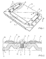
- the mounting plate 1 from FIG. 1 is made from a plate of uniform thickness, for example, made of an approximately 2 mm thick aluminum sheet.
- the Mounting plate 1 is first perforated, for example by drilling, to create the mounting holes 2.
- In a subsequent step become the upper surface side by cold working 10, d. H. the base of the mounting plate 1 outstanding and to this plane-parallel bearing surface 4 and the ring around the mounting openings 2 guided wells 3 formed.
- the recesses 3 are in the mounting plate by means of a stamp 1 pressed.
- FIG. 2 which is a sectional view of the mounting plate 1 along the section line A - A 'through one of the assembly openings 2, is formed by the formation of the recesses 3 material in the direction of respective mounting opening 2 shifted.
- This will make the material thickness y of the mounting plate 1 in the area of the mounting openings 2 by about 50% increased compared to the original thickness x of the mounting plate 1, in However, the area of the depressions 3 is reduced.
- the mounting plate 1 perpendicular to the base the mounting plate 1, moved so that under the recesses 3 on the lower surface side 11 of the mounting plate 1 annular material mountains 3 'arise that the lower surface 12 of the thickened areas overtop.
- the mounting plate 1 When handling the mounting plate 1 is through these mountains of material 3 'the risk of injury on the lower surface side 11 the mounting plate 1 resulting sharp edges of the wells 2 or the screws 5 screwed into the recesses 2 reduced.
- the mounting plate 1 forms a Lid for a housing, in which a populated with electronic components 7 Circuit carrier 6 is installed.
- the circuit carrier 6 is for this purpose with self-tapping screws 5, which go into the mounting holes 2 be screwed, connected to the mounting plate 1.
- the latter works at the same time as a heat sink, the thermal coupling between the Circuit carrier 6 and the mounting plate 1 is improved in that the circuit carrier 6 and the mounting plate 1 by means of a double-sided Adhesive tape 8, which before the assembly of the circuit carrier 6 applied to the degreased support surface 4 of the mounting plate 1 without bubbles will be glued together.
Landscapes
- Engineering & Computer Science (AREA)
- Microelectronics & Electronic Packaging (AREA)
- Physics & Mathematics (AREA)
- Thermal Sciences (AREA)
- Cooling Or The Like Of Electrical Apparatus (AREA)
- Cooling Or The Like Of Semiconductors Or Solid State Devices (AREA)
- Mounting Of Printed Circuit Boards And The Like (AREA)
- Connection Of Plates (AREA)
- Casings For Electric Apparatus (AREA)
- Shaping Metal By Deep-Drawing, Or The Like (AREA)
Claims (5)
- Procédé de fabrication d'une platine de montage (1), d'après lequel on augmente l'épaisseur de matériau de la platine de montage (1) dans la zone d'au moins une ouverture de montage (2) prévue pour le vissage d'une vis, par la formation à la presse d'au moins une empreinte en creux (3) adjacente à ladite zone.
- Procédé selon la revendication 1, caractérisé en ce que ladite au moins une empreinte en creux (3) est formée par matriçage à froid.
- Procédé selon la revendication 1 ou 2, caractérisé en ce que ladite au moins une empreinte en creux (3) entoure de manière annulaire ladite au moins une ouverture de montage (2).
- Procédé selon l'une des revendications 1 à 3, caractérisé en ce qu'au moins dans la zone de ladite au moins une ouverture de montage (2), est réalisée, par formage à la presse, une surface d'appui (14) qui est destinée à un support de circuit (6), et se situe à un niveau au-dessus de la surface d'une des faces (10) de la platine de montage (1) et est parallèle au plan de celle-ci.
- Procédé selon l'une des revendications précédentes, destiné à la fabrication d'une platine de montage (1) en tant que corps de refroidissement ou dissipateur de chaleur pour un composant électronique (7) ou un support de circuit (6) équipé de composants électroniques (7).
Applications Claiming Priority (2)
| Application Number | Priority Date | Filing Date | Title |
|---|---|---|---|
| DE19750433 | 1997-11-14 | ||
| DE19750433A DE19750433A1 (de) | 1997-11-14 | 1997-11-14 | Verfahren zur Erzeugung einer Montageplatte |
Publications (3)
| Publication Number | Publication Date |
|---|---|
| EP0917417A2 EP0917417A2 (fr) | 1999-05-19 |
| EP0917417A3 EP0917417A3 (fr) | 1999-12-15 |
| EP0917417B1 true EP0917417B1 (fr) | 2004-09-08 |
Family
ID=7848700
Family Applications (1)
| Application Number | Title | Priority Date | Filing Date |
|---|---|---|---|
| EP98120818A Expired - Lifetime EP0917417B1 (fr) | 1997-11-14 | 1998-11-03 | Procédé de fabrication d'une platine |
Country Status (5)
| Country | Link |
|---|---|
| US (1) | US6158266A (fr) |
| EP (1) | EP0917417B1 (fr) |
| JP (1) | JPH11254049A (fr) |
| DE (2) | DE19750433A1 (fr) |
| ES (1) | ES2226056T3 (fr) |
Families Citing this family (17)
| Publication number | Priority date | Publication date | Assignee | Title |
|---|---|---|---|---|
| FR2798814B1 (fr) * | 1999-09-22 | 2001-11-16 | Valeo Vision | Perfectionnements aux assemblages electroniques a drain thermique, notamment pour module de commande de lampe a decharge de projecteur de vehicule automobile |
| US6215663B1 (en) * | 2000-03-16 | 2001-04-10 | Philips Electronics North America Corporation | Printed circuit board assembly with improved thermal performance |
| DE10062699A1 (de) * | 2000-12-15 | 2002-07-04 | Conti Temic Microelectronic | Kühlvorrichtung für elektronische Steuergeräte |
| DE10109083B4 (de) * | 2001-02-24 | 2006-07-13 | Conti Temic Microelectronic Gmbh | Elektronische Baugruppe |
| US6588087B1 (en) * | 2001-10-02 | 2003-07-08 | Fisher Dynamics Corporation | Method of forming a side plate with integral boss |
| DE10206271A1 (de) * | 2002-02-15 | 2003-08-28 | Conti Temic Microelectronic | Wärmeableitvorrichtung |
| DE10300175B4 (de) * | 2003-01-08 | 2016-12-29 | Hella Kgaa Hueck & Co. | Elektronische Baugruppe mit Wärme ableitendem Gehäuseteil |
| JP4637926B2 (ja) | 2008-03-28 | 2011-02-23 | 日立オートモティブシステムズ株式会社 | 電子装置および液圧ユニット |
| JP5612321B2 (ja) * | 2010-01-27 | 2014-10-22 | 株式会社ヨロズ | スリーブ一体型メンバーとその製造方法 |
| US20130128182A1 (en) * | 2011-11-18 | 2013-05-23 | Shenzhen China Star Optoelectronics Technology Co., Ltd. | Back Frame of Flat Panel Display Device, Method for Manufacturing Back Frame, and Backlight System |
| US20130128420A1 (en) * | 2011-11-18 | 2013-05-23 | Shenzhen China Star Optoelectronics Technology Co. | Back Frame Of Flat Panel Display Device, Method For Manufacturing Back Frame, And Backlight System |
| US20130128139A1 (en) * | 2011-11-18 | 2013-05-23 | Shenzhen China Star Optoelectronics Technology Co. Ltd. | Flat Panel Display Device, Stereoscopic Display Device, Plasma Display Device |
| US20130128138A1 (en) * | 2011-11-18 | 2013-05-23 | Shenzhen China Star Optoelectronics Technolog Co., LTD. | Flat Panel Display Device, Stereoscopic Display Device, Plasma Display Device |
| US20130128147A1 (en) * | 2011-11-18 | 2013-05-23 | Shenzhen China Star Optoelectronics Technology Co., Ltd. | Flat Panel Display Device, Stereoscopic Display Device,and Plasma Display Device |
| US9820419B2 (en) | 2014-10-30 | 2017-11-14 | Crystal Group, Inc. | Apparatus and method for utilizing commercial off the shelf circuit boards in a highly kinematic environment |
| DE102015218937A1 (de) | 2015-09-30 | 2017-03-30 | Continental Teves Ag & Co. Ohg | Elektronischer Schaltungsträger, Kühlkörper und elektrische Vorrichtung |
| US20250081398A1 (en) * | 2023-08-31 | 2025-03-06 | Hamilton Sundstrand Corporation | Aluminum sheet with dielectric coating isolation barrier |
Family Cites Families (12)
| Publication number | Priority date | Publication date | Assignee | Title |
|---|---|---|---|---|
| US3611046A (en) * | 1966-09-16 | 1971-10-05 | Cross Electronics Inc | Apparatus for mounting and-or cooling electrical devices |
| DE2907415A1 (de) * | 1979-02-26 | 1980-09-04 | Wilhelm Schuetz | Verfahren und vorrichtung zur herstellung eines blechdurchzuges fuer muttergewinde |
| US4713960A (en) * | 1983-12-19 | 1987-12-22 | Gassaway J Scott | Method for forming a countersink in a plate |
| KR950014306B1 (ko) * | 1985-12-17 | 1995-11-24 | 유티카 엔터프라이지즈, 인코오포레이티드 | 차체 판넬(body panel) 성형 장치 및 그 방법 |
| JPH02137620A (ja) * | 1988-11-17 | 1990-05-25 | Tokin Corp | 金属スペーサ並びにその加工方法 |
| JPH03175698A (ja) * | 1989-12-04 | 1991-07-30 | Mitsubishi Electric Corp | プリント配線板 |
| JPH05243756A (ja) * | 1992-03-02 | 1993-09-21 | Nec Corp | 電子部品用アセンブリー |
| DE9406386U1 (de) * | 1994-04-16 | 1994-06-30 | Klöckner-Moeller GmbH, 53115 Bonn | Befestigungsplatte zum Aufrasten eines darauf montierten Niederspannungsschaltgerätes auf eine Hutschiene |
| JPH0856086A (ja) * | 1994-08-12 | 1996-02-27 | Fujitsu Ten Ltd | 配線基板の部材への取付構造 |
| US5581877A (en) * | 1994-09-30 | 1996-12-10 | Allen-Bradley Company, Inc. | Method of fabrication of a circuit board adapted to receive a single in-line module |
| JP3288875B2 (ja) * | 1994-11-28 | 2002-06-04 | 株式会社東芝 | シールドケースの取付構造 |
| JPH09260871A (ja) * | 1996-03-19 | 1997-10-03 | Kyocera Corp | 配線基板の組立構造 |
-
1997
- 1997-11-14 DE DE19750433A patent/DE19750433A1/de not_active Ceased
-
1998
- 1998-11-03 EP EP98120818A patent/EP0917417B1/fr not_active Expired - Lifetime
- 1998-11-03 ES ES98120818T patent/ES2226056T3/es not_active Expired - Lifetime
- 1998-11-03 DE DE59811919T patent/DE59811919D1/de not_active Expired - Lifetime
- 1998-11-10 JP JP10355286A patent/JPH11254049A/ja active Pending
- 1998-11-16 US US09/192,329 patent/US6158266A/en not_active Expired - Lifetime
Also Published As
| Publication number | Publication date |
|---|---|
| DE59811919D1 (de) | 2004-10-14 |
| EP0917417A2 (fr) | 1999-05-19 |
| ES2226056T3 (es) | 2005-03-16 |
| EP0917417A3 (fr) | 1999-12-15 |
| US6158266A (en) | 2000-12-12 |
| JPH11254049A (ja) | 1999-09-21 |
| DE19750433A1 (de) | 1999-06-02 |
Similar Documents
| Publication | Publication Date | Title |
|---|---|---|
| EP0917417B1 (fr) | Procédé de fabrication d'une platine | |
| EP1061783B2 (fr) | Substrat céramique-métal, notamment substrat multiple | |
| DE102012201172B4 (de) | Verfahren zur Herstellung eines Leistungshalbleitermoduls mit geprägter Bodenplatte | |
| EP0706214A2 (fr) | Module électronique et carte à puce | |
| DE4220966C2 (de) | Verfahren zum Herstellen einer Trägerplatte für elektrische Bauteile | |
| EP0844808B1 (fr) | Dispositif pour circuit imprimé | |
| DE3627372C3 (de) | Anordnung, bestehend aus einer Leiterplatte, einem Kühlkörper und zu kühlenden elektronischen Bauelementen | |
| DE3343034C2 (de) | Gehäuse für Halbleitervorrichtungen | |
| EP1887621A2 (fr) | Distributeur d'énergie doté d'un corps de refroidissement | |
| DE3445690C2 (de) | Verfahren zur Herstellung einer Trägerplatte für eine gedruckte Schaltung | |
| EP0490984B1 (fr) | Plaque cannelee d'estampage | |
| DE19852832C2 (de) | Verfahren zur Herstellung eines Metall-Kunststoff-Laminats | |
| DE19615481C5 (de) | Gewölbtes Metall-Keramik-Substrat | |
| EP0126856A2 (fr) | Procédé de fabrication d'une plaquette de circuit comportant des domaines rigides et flexibles | |
| WO2022128220A1 (fr) | Appareil destiné à contenir une unité d'alimentation et à centrer une unité de commande par rapport à l'unité d'alimentation | |
| DE102021109658B3 (de) | Verfahren zur Herstellung eines Halbleiter-Leistungsgeräts und damit hergestelltes Halbleiter-Leistungsgerät sowie ein Werkzeugteil für eine Sinterpresse und Verwendung einer Sinterpresse | |
| DE19912957B4 (de) | Scheibenbremsbelag mit einem Dämpfungsblech | |
| DE2752655A1 (de) | Elektronisches bauelement | |
| DE3315414C2 (fr) | ||
| EP0393496A2 (fr) | Substrat pour plaque de circuit électrique, composé de couches de cuivre et de couches de céramique | |
| DE19511486A1 (de) | Verfahren zur Herstellung einer Leiterplattenanordnung | |
| DE3624756C2 (fr) | ||
| EP0168722B1 (fr) | Elément d'écartement pour unité de cuisson ou évier en vitro-céramique | |
| DE3609239A1 (de) | Verfahren zur herstellung einer plattenartigen matrize | |
| DE2819031A1 (de) | Verfahren zur herstellung von ausschnitten in glasfaser - o.ae. - verstaerkten und/oder beschichteten kunststoffplatten sowie vorrichtung zur durchfuehrung dieses verfahrens |
Legal Events
| Date | Code | Title | Description |
|---|---|---|---|
| PUAI | Public reference made under article 153(3) epc to a published international application that has entered the european phase |
Free format text: ORIGINAL CODE: 0009012 |
|
| AK | Designated contracting states |
Kind code of ref document: A2 Designated state(s): DE ES FR GB IT SE |
|
| AX | Request for extension of the european patent |
Free format text: AL;LT;LV;MK;RO;SI |
|
| PUAL | Search report despatched |
Free format text: ORIGINAL CODE: 0009013 |
|
| AK | Designated contracting states |
Kind code of ref document: A3 Designated state(s): AT BE CH CY DE DK ES FI FR GB GR IE IT LI LU MC NL PT SE |
|
| AX | Request for extension of the european patent |
Free format text: AL;LT;LV;MK;RO;SI |
|
| 17P | Request for examination filed |
Effective date: 20000212 |
|
| RAP1 | Party data changed (applicant data changed or rights of an application transferred) |
Owner name: TEMIC TELEFUNKEN MICROELECTRONIC GMBH |
|
| AKX | Designation fees paid |
Free format text: DE ES FR GB IT SE |
|
| RAP1 | Party data changed (applicant data changed or rights of an application transferred) |
Owner name: CONTI TEMIC MICROELECTRONIC GMBH |
|
| GRAP | Despatch of communication of intention to grant a patent |
Free format text: ORIGINAL CODE: EPIDOSNIGR1 |
|
| GRAS | Grant fee paid |
Free format text: ORIGINAL CODE: EPIDOSNIGR3 |
|
| GRAA | (expected) grant |
Free format text: ORIGINAL CODE: 0009210 |
|
| REG | Reference to a national code |
Ref country code: SE Ref legal event code: TRGR |
|
| AK | Designated contracting states |
Kind code of ref document: B1 Designated state(s): DE ES FR GB IT SE |
|
| REG | Reference to a national code |
Ref country code: GB Ref legal event code: FG4D Free format text: NOT ENGLISH |
|
| GBT | Gb: translation of ep patent filed (gb section 77(6)(a)/1977) |
Effective date: 20040908 |
|
| REF | Corresponds to: |
Ref document number: 59811919 Country of ref document: DE Date of ref document: 20041014 Kind code of ref document: P |
|
| REG | Reference to a national code |
Ref country code: ES Ref legal event code: FG2A Ref document number: 2226056 Country of ref document: ES Kind code of ref document: T3 |
|
| PLBE | No opposition filed within time limit |
Free format text: ORIGINAL CODE: 0009261 |
|
| STAA | Information on the status of an ep patent application or granted ep patent |
Free format text: STATUS: NO OPPOSITION FILED WITHIN TIME LIMIT |
|
| ET | Fr: translation filed | ||
| 26N | No opposition filed |
Effective date: 20050609 |
|
| PGFP | Annual fee paid to national office [announced via postgrant information from national office to epo] |
Ref country code: ES Payment date: 20081121 Year of fee payment: 11 |
|
| PGFP | Annual fee paid to national office [announced via postgrant information from national office to epo] |
Ref country code: SE Payment date: 20081114 Year of fee payment: 11 Ref country code: IT Payment date: 20081122 Year of fee payment: 11 |
|
| PGFP | Annual fee paid to national office [announced via postgrant information from national office to epo] |
Ref country code: GB Payment date: 20081117 Year of fee payment: 11 |
|
| EUG | Se: european patent has lapsed | ||
| GBPC | Gb: european patent ceased through non-payment of renewal fee |
Effective date: 20091103 |
|
| PG25 | Lapsed in a contracting state [announced via postgrant information from national office to epo] |
Ref country code: GB Free format text: LAPSE BECAUSE OF NON-PAYMENT OF DUE FEES Effective date: 20091103 |
|
| REG | Reference to a national code |
Ref country code: ES Ref legal event code: FD2A Effective date: 20110304 |
|
| PG25 | Lapsed in a contracting state [announced via postgrant information from national office to epo] |
Ref country code: IT Free format text: LAPSE BECAUSE OF NON-PAYMENT OF DUE FEES Effective date: 20091103 |
|
| PG25 | Lapsed in a contracting state [announced via postgrant information from national office to epo] |
Ref country code: SE Free format text: LAPSE BECAUSE OF NON-PAYMENT OF DUE FEES Effective date: 20091104 |
|
| PG25 | Lapsed in a contracting state [announced via postgrant information from national office to epo] |
Ref country code: ES Free format text: LAPSE BECAUSE OF NON-PAYMENT OF DUE FEES Effective date: 20110303 |
|
| PG25 | Lapsed in a contracting state [announced via postgrant information from national office to epo] |
Ref country code: ES Free format text: LAPSE BECAUSE OF NON-PAYMENT OF DUE FEES Effective date: 20091104 |
|
| REG | Reference to a national code |
Ref country code: FR Ref legal event code: PLFP Year of fee payment: 18 |
|
| REG | Reference to a national code |
Ref country code: FR Ref legal event code: PLFP Year of fee payment: 19 |
|
| REG | Reference to a national code |
Ref country code: FR Ref legal event code: PLFP Year of fee payment: 20 |
|
| PGFP | Annual fee paid to national office [announced via postgrant information from national office to epo] |
Ref country code: DE Payment date: 20171130 Year of fee payment: 20 Ref country code: FR Payment date: 20171121 Year of fee payment: 20 |
|
| REG | Reference to a national code |
Ref country code: DE Ref legal event code: R071 Ref document number: 59811919 Country of ref document: DE |