EP0921462A2 - Arithmetische Einheit und Datenverarbeitungseinheit - Google Patents
Arithmetische Einheit und Datenverarbeitungseinheit Download PDFInfo
- Publication number
- EP0921462A2 EP0921462A2 EP98122838A EP98122838A EP0921462A2 EP 0921462 A2 EP0921462 A2 EP 0921462A2 EP 98122838 A EP98122838 A EP 98122838A EP 98122838 A EP98122838 A EP 98122838A EP 0921462 A2 EP0921462 A2 EP 0921462A2
- Authority
- EP
- European Patent Office
- Prior art keywords
- data
- signal
- output
- register
- memory
- Prior art date
- Legal status (The legal status is an assumption and is not a legal conclusion. Google has not performed a legal analysis and makes no representation as to the accuracy of the status listed.)
- Granted
Links
Images


Classifications
-
- G—PHYSICS
- G06—COMPUTING OR CALCULATING; COUNTING
- G06F—ELECTRIC DIGITAL DATA PROCESSING
- G06F12/00—Accessing, addressing or allocating within memory systems or architectures
-
- H—ELECTRICITY
- H03—ELECTRONIC CIRCUITRY
- H03M—CODING; DECODING; CODE CONVERSION IN GENERAL
- H03M7/00—Conversion of a code where information is represented by a given sequence or number of digits to a code where the same, similar or subset of information is represented by a different sequence or number of digits
- H03M7/30—Compression; Expansion; Suppression of unnecessary data, e.g. redundancy reduction
- H03M7/40—Conversion to or from variable length codes, e.g. Shannon-Fano code, Huffman code, Morse code
- H03M7/4006—Conversion to or from arithmetic code
-
- G—PHYSICS
- G06—COMPUTING OR CALCULATING; COUNTING
- G06F—ELECTRIC DIGITAL DATA PROCESSING
- G06F7/00—Methods or arrangements for processing data by operating upon the order or content of the data handled
- G06F7/02—Comparing digital values
-
- H—ELECTRICITY
- H03—ELECTRONIC CIRCUITRY
- H03M—CODING; DECODING; CODE CONVERSION IN GENERAL
- H03M7/00—Conversion of a code where information is represented by a given sequence or number of digits to a code where the same, similar or subset of information is represented by a different sequence or number of digits
- H03M7/30—Compression; Expansion; Suppression of unnecessary data, e.g. redundancy reduction
- H03M7/46—Conversion to or from run-length codes, i.e. by representing the number of consecutive digits, or groups of digits, of the same kind by a code word and a digit indicative of that kind
-
- G—PHYSICS
- G06—COMPUTING OR CALCULATING; COUNTING
- G06F—ELECTRIC DIGITAL DATA PROCESSING
- G06F2207/00—Indexing scheme relating to methods or arrangements for processing data by operating upon the order or content of the data handled
- G06F2207/02—Indexing scheme relating to groups G06F7/02 - G06F7/026
- G06F2207/025—String search, i.e. pattern matching, e.g. find identical word or best match in a string
Definitions
- the present invention relates to an arithmetic unit and a data processing unit mounted in a digital signal processor and the like.
- reference character 1x is a memory (8-bit-data memory with addresses 0 to 63)
- 2x is a read control circuit
- 3x is a zero run counter
- 4x is a zero decoder
- 5x is memory data
- 6x is a memory read control signal
- 7x is an enable signal
- 8x is a zero decode signal
- 9x is a zero run count signal.
- reference character 10x is a variable length encoder for performing variable length encoding.
- Waveform 1w in Figure 17 is used as the operating clock (CLK) of the data processing unit of Figure 16.
- the read control circuit 2x in Figure 16 reads out the memory data 5x at the address specified by the memory readout control signal 6x when the enable signal 7x is at a high level (hereinafter referred to as H level) (in the illustrated example, addresses are generated in the order of 0, 1, 2, ..., 63).
- the zero decoder 4x decodes the memory data 5x and, when the memory data shows a value 0, sets the zero decode signal 8x to the H level. At this time, the zero run counter 3x counts up, thus counting the number of 0s occurring consecutively. When the zero decode signal 8x is at a Low level (hereinafter referred to as the L level), the zero run counter 3x shows a value 0.
- variable length encoder circuit 10x at the following stage performs data processing using the zero run count signal 9x and memory data 5x at the time that the zero decode signal 8x is at the L level.
- Variable length encoding is a process in which data is compressed by treating the number of consecutive data zeros and the nonzero data following the data zeros as one set of data. Strictly speaking, quantization is performed before the variable length encoding.
- the zero run count signal 9x indicates the number of consecutive data zeros and the memory data 5x the nonzero data.
- the prior art data processing unit lacks versatility and cannot, for example, detect the number of consecutive data values other than zeros; further, when, for example, it becomes necessary to perform an addition or comparison in addition to sequentially detecting and outputting the number of consecutive data zeros and the nonzero data following the data zeros, extra circuitry for performing the addition or comparison has to be added.
- the prior art data processing unit when mounted as a special-purpose circuit in a digital signal processor or the like, is not able to continuously perform the data processing using the zero run count signal 9x and memory data 5x if zeros continue to appear in the memory data.
- the reason is that, since data compression is performed using both the number of consecutive zeros and the nonzero data, it is not possible to produce the output of the zero run counter 3x and the output of the nonzero data in every cycle.
- the prior art data processing unit has also had the problems that it lacks versatility because it is designed for performing data processing on fixed data (in the above example, data zeros), and that the processing time increases since data retrieval is performed through the entire memory even in the case of data that may be all zeros beyond a certain memory range.
- a first arithmetic unit of the present invention comprises a comparator circuit, a shifter, an adder circuit, a register, and a selection circuit.
- the comparator circuit takes as inputs first data as comparison reference data and second data as data to be compared with the first data, and performs a comparison between the first and the second data; when the first and the second data match as the result of the comparison, the comparator circuit outputs a value 1 and sets a match signal active, while, when the first and the second data do not match, the comparator circuit outputs the second data and sets the match signal inactive.
- the shifter accepts an output of the comparator circuit at its input, and shifts, or does not shift, the output of the comparator circuit, depending on the state of the match signal supplied from the comparator circuit.
- the adder circuit accepts an output of the shifter at one input thereof.
- the register accepts an output of the adder circuit at its input.
- the selection circuit accepts a value 0 at one input thereof and an output of the register at the other input, and couples one or the other of its inputs to the other input of the adder circuit in accordance with a selection signal.
- the selection circuit selecting either the value 0 or the output of the register in accordance with the selection signal, when the first and the second data do not match, the second data that does not match the first data is output by being paired with a count of the number of times that the second data matched the first data since the last occurrence of a mismatch between the first and the second data.
- the comparator circuit for performing a comparison between the first and second data
- the shifter for accepting the output of the comparator circuit at its input, and for shifting or not shifting the output of the comparator circuit depending on the state of the match signal supplied from the comparator circuit
- the adder circuit for cumulatively adding the output of the shifter, and the selection circuit, not only can the processing to sequentially detect and output the number of consecutive data zeros and the nonzero data following the data zeros be performed, but similar processing can also be performed on data of values other than zero. This provides great versatility.
- a second arithmetic unit of the present invention comprises a comparator circuit, a flag register, a first register, a shifter, a second register, a third register, and a selection circuit.
- the comparator circuit takes as inputs first data as comparison reference data and second data as data to be compared with the first data, and performs a comparison between the first and the second data; when the first and the second data match as the result of the comparison, the comparator circuit outputs a value 1 and sets a match signal active, while, when the first and the second data do not match, the comparator circuit outputs the second data and sets the match signal inactive.
- the flag register accepts the match signal at its input.
- the first register accepts an output of the comparator circuit at its input.
- the shifter accepts an output of the first register at its input, and shifts, or does not shift, the output of the first register, depending on the state of the match signal supplied from the flag register.
- the second register accepts an output of the shifter at its input.
- the adder circuit accepts an output of the second register at one input thereof.
- the third register accepts an output of the adder circuit at its input.
- the selection circuit accepts a value 0 at one input thereof and an output of the third register at the other input, and couples one or the other of its inputs to the other input of the adder circuit in accordance with a selection signal.
- the selection circuit selecting either the value 0 or the output of the third register in accordance with the selection signal, when the first and the second data do not match, the second data that does not match the first data is output by being paired with a count of the number of times that the second data matched the first data since the last occurrence of a mismatch between the first and the second data.
- the interposition of the first and second registers and the flag register between the comparator circuit, the shifter, and the adder circuit offers an additional effect; that is, with this arrangement, if the comparator circuit, the shifter, and the adder circuit are not fast in operation, not only can the processing to sequentially detect and output the number of consecutive data zeros and the nonzero data following the data zeros be performed, but similar processing can also be performed on data of values other than zero.
- a first data processing unit comprises: a control unit which, when executing an instruction, outputs a memory read control signal, a memory write control signal, an instruction execution signal, a comparison reference data setting signal, and an end flag signal; a first memory to which the memory read control signal is input; a first data register to which the comparison reference data setting signal is input to set comparison reference data therein; a second data register which stores data from the first memory; a number-of-retrievals counter to which the instruction execution signal is input, and which outputs to the control unit a count of the number of data retrievals so far performed on the first memory; an execution unit to which the instruction execution signal and output data from the first data register and the second data register are input, and which outputs a comparison signal and an execution data signal; and a second memory to which the memory write control signal, the execution data signal from the execution unit, and the end flag signal are input.
- the control unit terminates the comparison instruction and sets the end flag signal active, while the comparison signal from the execution unit is output to the control unit to control writing to the second memory so that the end flag signal and the execution data signal, indicating the number of times that the output data matched and data from the first memory that did not match the comparison reference data, are written to the second memory when the end flag signal is held inactive and also when the end flag signal is set active.
- the comparison instruction can be executed for any given value by setting desired comparison reference data in the first data register, and can be terminated by the action of the number-of-retrievals counter counting the number of retrievals performed within the comparison range, and the end flag signal can thus be written to the second memory, so that the last written data can be detected by just reading the data written in the second memory.
- variable length encoding instruction can be executed any time without having to be limited to the time at which a count of the number of times the comparison data matched and the data that did not match, based on which variable length encoding is performed, are latched.
- the execution unit when configured to have other functions than the detection of the number of values 0, since it has a path via which to store data in the second memory, the execution unit of such a configuration can also be used without losing its versatility.
- variable length encoded data since the data before variable length encoding is held in the second memory, it is possible to verify whether or not the variable length encoded data has been correctly converted by comparing the variable length encoded data with the data held in the second memory, and the variable length encoded data can thus be debugged.
- the last written data earlier mentioned refers to the data that was written at the last address when comparing data in the first memory, for example, from a certain address to a certain address.
- the execution of the comparison instruction is terminated, and the end flag signal is written to the second memory.
- a second data processing unit of the present invention comprises: a control unit which, when executing an instruction, outputs a memory read control signal, a memory write control signal, an instruction execution signal, a comparison reference data setting signal, and an end flag signal; a first memory to which the memory read control signal is input; a first data register to which the comparison reference data setting signal is input to set comparison reference data therein; a second data register which stores data from the first memory; a number-of-retrievals counter to which the instruction execution signal is input, and which outputs to the control unit a count of the number of data retrievals so far performed on the first memory; an execution unit to which the instruction execution signal and output data from the first data register and the second data register are input, and which outputs a comparison signal and an execution data signal; a second memory to which the memory write control signal and the execution data signal from the execution unit are input; and a third data register to which the end flag signal is input, and which stores the address of data stored in the second memory.
- the control unit terminates the comparison instruction and sets the end flag signal active, while the comparison signal from the execution unit is output to the control unit to control writing to the second memory so that the end flag signal and the execution data signal, indicating the number of times that the output data matched and data from the first memory that did not match the comparison reference data, are written to the second memory when the end flag signal is held inactive and also when the end flag signal is set active, and so that the address last written to the second memory is stored in the third data register when the end flag signal is set active.
- the comparison instruction can be executed for any given value by setting desired comparison reference data in the first data register, and can be terminated by the action of the number-of-retrievals counter counting the number of retrievals performed within the comparison range, and the end flag signal can thus be generated and the memory address be stored in the third data register functioning as a memory address setting register; accordingly, the memory address where the last written data is stored can be detected by just reading the data from the third data register.
- any data can be handled by setting any given value in the first data register, and the versatility is thus increased.
- a third data processing unit of the present invention comprises: a control unit which, when executing an instruction, outputs a memory read control signal, a memory write control signal, an instruction execution signal, a comparison reference data setting signal, an end flag signal, and a number-of-retrievals setting signal; a first memory to which the memory read control signal is input; a first data register to which the comparison reference data setting signal is input to set comparison reference data therein; a second data register which stores data from the first memory; a number-of-retrievals counter to which the instruction execution signal is input, and which outputs a count of the number of data retrievals so far performed on the first memory; a third data register to which the number-of-retrievals setting signal is input to set therein an end value for the number of retrievals; an execution unit to which the instruction execution signal and output data from the first data register and the second data register are input, and which outputs a comparison signal and an execution data signal; a second memory to which the memory write control signal, the execution data
- the output data from the first data register and the second data register are loaded by the instruction execution signal into the execution unit for data comparison and, at the same time, the number-of-retrievals counter is made to count up, wherein the end flag signal is held inactive until the match signal is output from the match detection circuit and, in response to the match signal output from the match detection circuit, the control unit terminates the comparison instruction and sets the end flag signal active, while the comparison signal from the execution unit is output to the control unit to control writing to the second memory so that the end flag signal and the execution data signal, indicating the number of times that the output data matched and data from the first memory that did not match the comparison reference data, are written to the second memory when the end flag signal is held inactive and also when the end flag signal is set active.
- the third data processing unit is capable of executing the comparison instruction for any given value by setting desired comparison reference data in the first data register, and can arbitrarily set the number of retrievals, to be performed within the comparison range, in the third data register, so that the comparison instruction can be terminated after performing an arbitrary number of retrievals. Since the end flag signal can thus be written to the second memory, the last written data can be detected by just reading out the data written to the second memory.
- any data can be handled by setting desired values in the third data register and the first data register, and the versatility is thus increased.
- a fourth data processing unit of the present invention comprises: a control unit which, when executing an instruction, outputs a memory read control signal, a memory write control signal, an instruction execution signal, a comparison reference data setting signal, an end flag signal, a number-of-retrievals setting signal, and a selection signal; a first memory to which the memory read control signal is input; a first data register to which the comparison reference data setting signal is input to set comparison reference data therein; a second data register which stores data from the first memory; a third data register to which the number-of-retrievals setting signal is input to set therein an initial value for the number of retrievals; a number-of-retrievals counter to which the instruction execution signal and output data from the third data register are input, and which outputs a count of the remaining number of retrievals to be performed on the first memory; an execution unit to which the instruction execution signal and output data from the first data register and the second data register are input, and which outputs a comparison signal and an execution data signal; an add
- the control unit terminates the comparison instruction and sets the end flag signal active, while the comparison signal from the execution unit is output to the control unit to control writing to the second memory so that the end flag signal and the execution data signal, indicating the number of times that the output data matched and data from the first memory that did not match the comparison reference data, are written to the second memory when the
- the fourth data processing unit is capable of executing the comparison instruction for any given value by setting desired comparison reference data in the first data register, and can arbitrarily set the number of retrievals, to be performed within the comparison range, in the third data register, so that the comparison instruction can be terminated after performing an arbitrary number of retrievals. Furthermore, when data matches occur consecutively, the comparison instruction can be terminated by assuming that the remaining data also match the comparison reference data, thus shortening the entire retrieval time. Since the end flag signal is thus written to the second memory, the last written data can be detected by just reading out the data written to the second memory.
- any data can be handled by setting desired values in the number-of-retrievals counter and the first data register, and the versatility is thus increased.
- a fifth data processing unit of the present invention comprises: a control unit which, when executing an instruction, outputs a memory read control signal, a memory write control signal, an instruction execution signal, a comparison reference data setting signal, an end flag signal, a number-of-retrievals setting signal, a number-of-consecutive-matches setting signal, and a selection signal; a first memory to which the memory read control signal is input; a first data register to which the comparison reference data setting signal is input to set comparison reference data therein; a second data register which stores data from the first memory; a third data register to which the number-of-retrievals setting signal is input to set therein an initial value for the number of retrievals; a fourth data register to which the number-of-consecutive-matches setting signal is input to set the number of times that data matches may occur consecutively; a number-of-retrievals counter to which the instruction execution signal and output data from the third data register are input, and which outputs a count of
- the control unit terminates the comparison instruction and sets the end flag signal active, while the comparison signal from the execution unit is output to the control unit to control writing to the second memory so that the end flag signal and the execution data signal, indicating the number of times that the output data matched and data from the first memory that did not match the comparison reference data, are written to the second memory when the end flag signal is held inactive and also when the end flag signal is set active, and so that, when
- the fifth data processing unit is capable of executing the comparison instruction for any given value by setting desired comparison reference data in the first data register, and can arbitrarily set the number of retrievals, to be performed within the comparison range, in the third data register, so that the comparison instruction can be terminated after performing an arbitrary number of retrievals. Furthermore, by presetting the desired number of matches in the fourth data register, when data matches occur consecutively the preset number of times, the comparison instruction can be terminated by assuming that the remaining data also match the comparison reference data, thus shortening the entire retrieval time. Since the end flag signal is thus written to the second memory, the last written data can be detected by just reading out the data written to the second memory.
- a sixth data processing unit of the present invention is the same as the first, second, third, fourth, of fifth data processing unit of the present invention, wherein the execution unit comprises: a comparator circuit which takes as inputs the output of the first data register as first data to serve as comparison reference data and the output of the second data register as second data to be compared with the first data, and performs a comparison between the first and the second data, and which, when the first and the second data match as the result of the comparison, outputs a value 1 and sets a match signal active, and when the first and the second data do not match, outputs the second data and sets the match signal inactive; a shifter to which an output of the comparator circuit is input, and which shifts, or does not shift, the output of the comparator circuit, depending on the state of the match signal supplied from the comparator circuit; an adder circuit which accepts an output of the shifter at one input thereof; a register to which an output of the adder circuit is input; and a selection circuit which accepts a value 0 at one input
- the selection circuit selecting either the value 0 or the output of the register in accordance with the selection signal, when the first and the second data do not match, the second data that does not match the first data is output as the execution data signal by being paired with a count of the number of times that the second data matched the first data since the last occurrence of a mismatch between the first and the second data.
- the same effects as obtained with the first arithmetic unit of the present invention can be achieved in addition to the effects obtained with the first, second, third, fourth, or fifth data processing unit of the present invention.
- a seventh data processing unit of the present invention is the same as the first, second, third, fourth, or fifth data processing unit of the present invention, wherein the execution unit comprises: a comparator circuit which takes as inputs the output of the first data register as first data to serve as comparison reference data and the output of the second data register as second data to be compared with the first data, and performs a comparison between the first and the second data, and which, when the first and the second data match as the result of the comparison, outputs a value 1 and sets a match signal active, and when the first and the second data do not match, outputs the second data and sets the match signal inactive; a flag register to which the match signal is input; a first register to which an output of the comparator circuit is input; a shifter to which an output of the first register is input, and which shifts, or does not shift, the output of the first register, depending on the state of the match signal supplied from the flag register; a second register to which an output of the shifter is input; an adder circuit which accepts an output
- the selection circuit selecting either the value 0 or the output of the third register in accordance with the selection signal, when the first and the second data do not match, the second data that does not match the first data is output as the execution data signal by being paired with a count of the number of times that the second data matched the first data since the last occurrence of a mismatch between the first and the second data.
- the same effects as obtained with the second arithmetic unit of the present invention can be achieved in addition to the effects obtained with the first, second, third, fourth, or fifth data processing unit of the present invention.
- Figure 1 is a block diagram showing the configuration of the arithmetic unit according to the first embodiment of the present invention.
- reference character 1A is a comparator circuit
- 2A is an 8-bit first register
- 3A is a flag register
- 4A is a shifter
- 5A is a 9-bit second register
- 6A is a selection circuit
- 7A is an adder circuit for performing cumulative additions
- 8A is a 14-bit third register.
- the comparator circuit 1A performs a comparison between the first data (waveform 3B in Figure 2, value 0 in HEX) and second data (waveform 2B in Figure 2) output in synchronism with the rising of an operating clock (waveform 1B in Figure 2) and, when the value of the second data is 0, sets a match signal to a high level and outputs it to the flag register 3A which latches it (waveform 7B in Figure 2) in synchronism with the rising of the operating clock.
- the comparator circuit 1A outputs a value 1 (waveform 4B in Figure 2) to the first register 2A which latches it (waveform 6B in Figure 2) in synchronism with the rising of the operating clock.
- the comparator circuit 1A sets the match signal (waveform 5B in Figure 2) to a low level and outputs it to the flag register 3A which latches it (waveform 7B in Figure 2) in synchronism with the rising of the operating clock.
- the comparator circuit 1A outputs the second data (waveform 4B in Figure 2) to the first register 2A which latches it (waveform 6B in Figure 2) in synchronism with the rising of the operating clock.
- the shifter 4A shifts the value of the first register 2A (waveform 6B in Figure 2) by 8 bits to the left, and outputs the resulting value 100 (in HEX, waveform 8B in Figure 2) to the second shift register 5A (waveform 8B in Figure 2) which latches it (waveform 9B in Figure 2) in synchronism with the rising of the operating clock.
- the shifter 2A does not shift the value of the first register 2A (waveform 6B in Figure 2), but outputs the value of the first register 2A unchanged (waveform 8B in Figure 2) to the second register 5A which latches it (waveform 9B in Figure 2) in synchronism with the rising of the operating clock.
- the selection circuit 6A outputs a value 0 (waveform 10B in Figure 2) when a selection signal (waveform 12B in Figure 2) is at the low level and, when it is at the high level, selects the output of the third register 8A (waveform 11B in Figure 2) which latches the output of the adder circuit 7A in synchronism with the rising of the clock.
- the adder circuit 7A takes as inputs the output of the second register 5A (waveform 9B in Figure 2) and the output of the selection circuit 6A (waveform 10B in Figure 2), adds them together, and outputs the result of the addition to the third register 8A for accumulation.
- the third register 8A must be initialized before performing a series of arithmetic operations, and the value when the selection signal is low is output as the result of the calculation from the arithmetic unit.
- the low order 8 bits indicate nonzero data and the high order 6 bits represents a count of the number of consecutive zeros.
- This arithmetic unit is capable of performing the above-described operations not only on data of value zero but also on every other data by changing the value of the first data, and is also capable of using only the function of the comparator circuit 1A by controlling the shifter 4A, adder circuit 7A, and selection circuit 6A, only the function of the shifter 4A by controlling the comparator circuit 1A, adder circuit 7A, and selection circuit 6A, or only the function of the adder circuit 7A by controlling the comparator circuit 1A, shifter 4A, and selection circuit 6A. This adds great versatility to the arithmetic unit.
- the comparator circuit 1A, the shifter 4A, and the adder circuit 7A are not fast in operation, not only can the processing to sequentially detect and output the number of consecutive data zeros and the nonzero data following the data zeros be performed, but similar processing can also be performed on data of values other than zero.
- the first register 2A and flag register 3A are arranged between the comparator circuit 1A and the shifter 4A, and the second register 5A between the shifter 4A and the adder circuit 7A, but if further advances are made in miniaturization in the design of the arithmetic unit, achieving faster operations of the comparator circuit 1A, shifter 4A, and adder circuit 7A, it will become possible to omit the first register 2A, flag register 3A, and second register 5A.
- Figure 1 is a block diagram showing the configuration of the arithmetic unit according to the second embodiment of the present invention.
- the configuration is the same as that described in the first embodiment, the only difference from the first embodiment being that the 9-bit second register 5A is replaced with a 14-bit register.
- the comparator circuit 1A performs a comparison between the first data (waveform 3C in Figure 3, value 0 in HEX) and second data (waveform 2C in Figure 3) output in synchronism with the rising of the operating clock (waveform 1C in Figure 3) and, when the value of the second data is 0, sets the match signal to a high level and outputs it to the flag register 3A which latches it (waveform 7C in Figure 3) in synchronism with the rising of the operating clock.
- the comparator circuit 1A outputs a value 1 (waveform 4C in Figure 3) to the first register 2A which latches it in synchronism with the rising of the operating clock.
- the comparator circuit 1A sets the match signal (waveform 5C in Figure 3) to a low level and outputs it to the flag register 3A which latches it (waveform 7C in Figure 3) in synchronism with the rising of the operating clock.
- the comparator circuit 1A outputs the second data (waveform 4C in Figure 3) to the first register 2A which latches it in synchronism with the rising of the operating clock.
- the shifter 4A shifts the value of the first register 2A (waveform 6C in Figure 3) by 6 bits to the left, and outputs the resulting value (in HEX, waveform 8C in Figure 3) to the second shift register 5A (waveform 8C in Figure 3) which latches it (waveform 9C in Figure 3) in synchronism with the rising of the operating clock.
- the shifter 2A does not shift the value of the first register 2A (waveform 6C in Figure 3), but outputs the value of the first register 2A unchanged, that is, the value 1 (waveform 8C in Figure 3), to the second register 5A which latches it (waveform 9C in Figure 3) in synchronism with the rising of the operating clock .
- the selection circuit 6A outputs a value 0 (waveform 10C in Figure 3) when the selection signal (waveform 12C in Figure 3) is at the low level and, when it is at the high level, selects the output of the third register 8A (waveform 11C in Figure 3) which latches the output of the adder circuit 7A in synchronism with the rising of the clock.
- the adder circuit 7A takes as inputs the output of the second register 5A (waveform 9C in Figure 3) and the output of the selection circuit 6A (waveform 10C in Figure 3), adds them together, and outputs the result of the addition to the third register 8A for accumulation.
- the third register 8A must be initialized before performing a series of arithmetic operations, and the value when the selection signal is low is output as the result of the calculation from the arithmetic unit.
- the high order 8 bits indicate nonzero data and the low order 6 bits represents a count of the number of consecutive zeros.
- the arithmetic unit like the one in the foregoing first embodiment, has greatly increased versatility.
- the second embodiment has the potential of being able to omit the first and second registers 2A and 5A and flag register 3A; in that case, the one-cycle delay through the first and second registers 2A and 5A and flag register 3A would be eliminated, as in the case of the first embodiment.
- Embodiments of a data processing unit incorporating the arithmetic unit described in the first and second embodiments as a major constituent element of an execution unit will be described below.
- a data processing unit according to a third embodiment of the present invention will be described with reference to Figures 4 to 6.
- Figure 4 is a block diagram showing the configuration of the data processing unit according to the third embodiment of the present invention.
- reference character 1 is a control unit
- 2 is an execution unit
- 3 is a first memory
- 4 is a second memory
- 5 is a first data register as an 8-bit comparison reference data setting register
- 6 is a second data register as an 8-bit memory data register
- 7 is a number-of-retrievals counter.
- the first data in the arithmetic unit of Figure 1 is temporarily stored in the first data register 5, and likewise, the second data is temporarily stored in the second data register 6.
- reference character 8 is an instruction execution signal
- 9 is a comparison reference data setting signal
- 10 is a memory read control signal
- 11 is an end flag signal
- 12 is a memory write control signal
- 13 is a comparison signal
- 14 is an output signal of the number-of-retrievals counter 7
- 15 is a memory data signal
- 16 is an output signal of the first data register 5
- 17 is an output signal of the second data register 6,
- 18 is an execution data signal.
- the comparison signal 13 corresponds to the match signal output from the comparator circuit 1A or the output of the flag register 3A in the arithmetic unit of Figure 1.
- the first memory 3 is organized as an 8-bit-data memory with addresses 0 to 63, and the second memory 4 as a 15-bit-data memory with addresses 0 to 63, while the number-of-retrievals counter 7 counts from 0 to 64.
- Figure 5 is a diagram showing operating waveforms of the data processing unit according to the third embodiment of the present invention
- Figure 6 is a diagram showing the contents of the second memory 4 at the completion of writing, wherein reference character 1z indicates the memory address (in decimal), 2z the memory data, 3z the number of matches, and 4z the end flag.
- the memory data 2z is the data written without being shifted in the arithmetic unit of Figure 1, and the number of matches, 3z, is the data written after being shifted in the arithmetic unit of Figure 1.
- the position of the memory data 2z maybe interchanged with the position of the number of matches, 3z, depending on how the shifter in the arithmetic unit is set up.
- Waveform 1w in Figure 5 will be used as the operating clock (CLK) of the data processing unit of Figure 4, and the data processing unit of Figure 4 will be described as operating in synchronism with the rising edge of the operating clock 1w.
- the control unit 1 sets the instruction execution signal 8 (waveform 2w in Figure 5) to the H level to execute a comparison instruction.
- the control unit 1 outputs the memory read control signal 10, in response to which the memory data signal 15 at the address specified by the memory read address signal (waveform 3w in Figure 5) carried in the control signal 10 is read out of the first memory 3 and stored in the second data register 6 (waveform 4w in Figure 5).
- comparison reference data is set in the first data register 5 by using the comparison reference data setting signal 9 (waveform 5w in Figure 5; comparison reference data value is 0).
- the execution unit 2 compares the output signal 17 (waveform 4w in Figure 5) of the second data register 6 with the output signal 16 (waveform 5w in Figure 5) of the first data register 5 and, when they match, outputs the comparison signal 13 to the control unit 1, thereby setting the memory write control signal 12 (waveform 6w in Figure 5), to be output from the control unit 1, to the H level to inhibit writing to the second memory 4 and count the number of consecutive matches.
- the execution unit 2 When they do not match, on the other hand, the execution unit 2 writes its result signal (waveform 7w in Figure 5) as the execution data signal 18, together with the end flag signal 11 (waveform 9w in Figure 5), to the second memory 4 at the address (single address) specified by the memory write address signal (waveform 8w in Figure 5) carried in the memory write control signal 12.
- control unit 1 sets the instruction execution signal 8 to the L level to terminate the comparison instruction and, at the same time, sets the end flag signal 11 to the H level.
- the memory address 1z corresponds to the waveform 8w in Figure 5
- the 8-bit memory data z in bit positions from 0 to 7 corresponds to the waveform 4w in Figure 5
- the 6-bit match count data (the number of matches) 3z in bit positions from 8 to 13 corresponds to the waveform 7w in Figure 5
- the end flag 4z in the 14th bit position corresponds to the waveform 9w in Figure 5.
- the comparison instruction can be executed for any given value by setting desired comparison reference data in the first data register 5 functioning as a comparison reference data setting register, and can be terminated by the action of the number-of-retrievals counter 7 counting the number of retrievals performed within the comparison range, and the end flag signal 11 can thus be written to the second memory 4, so that the last written data can be detected by just reading the data written in the second memory 4.
- variable length encoding instruction can be executed any time without having to be limited to the time at which a count of the number of times the comparison data matched and the data that did not match, based on which variable length encoding is performed, are latched.
- the execution unit 2 when the execution unit 2 is configured to have other functions than the detection of the number of values 0, since it has a path via which to store data in the second memory 4, the execution unit 2 of such a configuration can also be used without losing its versatility.
- variable length encoded data since the data before variable length encoding is held in the second memory 4, it is possible to verify whether or not the variable length encoded data has been correctly converted by comparing the variable length encoded data with the data held in the second memory 4, and the variable length encoded data can thus be debugged.
- the last written data earlier mentioned refers to the data that was written at the last address when comparing data in the first memory 3, for example, from a certain address to a certain address.
- the execution of the comparison instruction is terminated, and the end flag signal 11 is written to the second memory 4.
- the data processing unit is equally implementable if data from some other memory is input as the comparison reference data to the first data register 5. That is, in the above-described configuration, the data from the first memory 3 is compared with the value from the data register 5; this means that data from some other memory may be written to the data register 5 and the data from the first memory 5 may be compared with the value from that other memory.
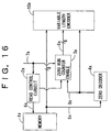
- a data processing unit according to a fourth embodiment of the present invention will be described with reference to Figures 7 and 8.
- Figure 7 is a block diagram showing the configuration of the data processing unit according to the fourth embodiment of the present invention.
- reference character 4a is a second memory
- 19 is a third data register as a 6-bit memory address storage register.
- control unit 1, execution unit 2, first memory 3, first data register 5, second data register 6, and number-of-retrievals counter 7 are essentially the same in configuration as the corresponding elements in the third embodiment shown in Figure 4. Differences from the third embodiment are that the second memory 4a is a 14-bit-data memory with addresses 0 to 63, and that the third data register 19 as a memory address storage register is additionally provided.
- Figure 8 is a diagram showing operating waveforms of the data processing unit according to the fourth embodiment of the present invention.
- Waveform 1w in Figure 8 will be used as the operating clock (CLK) of the data processing unit of Figure 7, and the data processing unit of Figure 7 will be described as operating in synchronism with the rising edge of the operating clock 1w.
- the control unit 1 sets the instruction execution signal 8 (waveform 2w in Figure 8) to the H level to execute the comparison instruction.
- the control unit 1 outputs the memory read control signal 10, in response to which the memory data signal 15 at the address specified by the memory read address signal (waveform 3w in Figure 8) carried in the control signal 10 is read out of the first memory 3 and stored in the second data register 6 (waveform 4w in Figure 8).
- comparison reference data is set in the first data register 5 by using the comparison reference data setting signal 9 (waveform 5w in Figure 8; comparison reference data value is 0).
- the execution unit 2 compares the output signal 17 (waveform 4w in Figure 8) of the second data register 6 with the output signal 16 (waveform 5w in Figure 8) of the first data register 5 and, when they match, outputs the comparison signal 13 to the control unit 1, thereby setting the memory write control signal 12 (waveform 6w in Figure 8), to be output from the control unit 1, to the H level to inhibit writing to the second memory 4a and count the number of consecutive matches.
- the execution unit 2 When they do not match, on the other hand, the execution unit 2 writes its result signal (waveform 7w in Figure 8) as the execution data signal 18, together with the end flag signal 11 (waveform 9w in Figure 8), to the second memory 4a at the address (single address) specified by the memory write address signal (waveform 8w in Figure 8) carried in the memory write control signal 12.
- the control unit 1 stores the address then indicated by the memory write address signal (waveform 8w in Figure 8) carried in the memory write control signal 12 into the third data register 19 (waveform 11w in Figure 8), and sets the instruction execution signal 8 to the L level to terminate the comparison instruction, while, at the same time, setting the end flag signal 11 (waveform 9w in Figure 8) to the H level.
- the comparison instruction can be executed for any given value by setting desired comparison reference data in the first data register 5 functioning as a comparison reference data setting register, and can be terminated by the action of the number-of-retrievals counter 7 counting the number of retrievals performed within the comparison range, and the end flag signal 11 can thus be generated and the memory address at that time be stored in the third data register 19 functioning as a memory address setting register; accordingly, the memory address where the last written data is stored can be detected by just reading the data from the third data register 19.
- any data can be handled by setting any given value in the first data register 5, and the versatility is thus increased.
- the data processing unit is equally implementable if data from some other memory is input as the comparison reference data to the first data register 5.
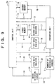
- a data processing unit according to a fifth embodiment of the present invention will be described with reference to Figures 9 and 10.
- Figure 9 is a block diagram showing the configuration of the data processing unit according to the fifth embodiment of the present invention.
- reference character 1a is a control unit
- 20 is a third data register as a 7-bit retrieval count number setting register
- 21 is a match detection circuit
- 22 is a retrieval count number setting signal
- 23 is an output signal of the third data register 20
- 24 is a match detection signal.
- the execution unit 2 In the data processing unit of the fifth embodiment, the execution unit 2, first memory 3, second memory 4, first data register 5, second data register 6, and number-of-retrievals counter 7 are essentially the same in configuration as the corresponding elements in the third embodiment shown in Figure 4. Differences from the third embodiment are that the control unit 1a takes as an input the match detection signal 24, not the output signal 14 of the number-of-retrievals counter 7, that the control unit 1a additionally outputs the retrieval count number setting signal 22, and that the third data register 20 and match detection circuit 21 are additionally provided.
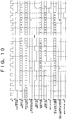
- Figure 10 is a diagram showing operating waveforms of the data processing unit according to the fifth embodiment of the present invention.
- Waveform 1w in Figure 10 will be used as the operating clock (CLK) of the data processing unit of Figure 9, and the data processing unit of Figure 9 will be described as operating in synchronism with the rising edge of the operating clock 1w.
- the control unit 1a sets the instruction execution signal 8 (waveform 2w in Figure 10) to the H level to execute the comparison instruction.
- the control unit 1a outputs the memory read control signal 10, in response to which the memory data signal 15 at the address specified by the memory read address signal (waveform 3w in Figure 10) carried in the control signal 10 is read out and stored in the second data register 6 (waveform 4w in Figure 10).
- comparison reference data Prior to the execution of the comparison instruction, comparison reference data is set in the first data register 5 by using the comparison reference data setting signal 9 (waveform 5w in Figure 10; comparison reference data value is 0), and a retrieval count number (an end value for the number of retrievals) is set in the third data register 20 by using the retrieval count number setting signal 22 (waveform 12w in Figure 10; retrieval count number is 64).
- the execution unit 2 compares the output signal 17 (waveform 4w in Figure 10) of the second data register 6 with the output signal 16 (waveform 5w in Figure 10) of the first data register 5 and, when they match, outputs the comparison signal 13 to the control unit 1a, thereby setting the memory write control signal 12 (waveform 6w in Figure 10), to be output from the control unit 1a, to the H level to inhibit writing to the second memory 4 and count the number of consecutive matches.
- the execution unit 2 When they do not match, on the other hand, the execution unit 2 writes its result signal (waveform 7w in Figure 10) as the execution data signal 18, together with the end flag signal 11 (waveform 9w in Figure 10), to the second memory 4 at the address (single address) specified by the memory write address signal (waveform 8w in Figure 10) carried in the memory write control signal 12.
- the match detection circuit 21 detects whether or not the output signal 14 (waveform 10w in Figure 10) of the number-of-retrievals counter 7 matches with the output signal 23 of the third data register 20 and, when both output signals 14 and 23 indicate value 64, sets the match detection signal 24 to the H level for output (waveform 13w in Figure 10).
- the control unit 1a sets the instruction execution signal 8 to the L level to terminate the comparison instruction, and at the same time, sets the end flag signal (waveform 9w in Figure 10) to the H level.
- the data processing unit of the fifth embodiment is capable of executing the comparison instruction for any given value by setting desired comparison reference data in the first data register 5 functioning as a comparison reference data setting register, and can arbitrarily set the number of retrievals, to be performed within the comparison range, in the third data register 20 functioning as a retrieval count number setting register, so that the comparison instruction can be terminated after performing an arbitrary number of retrievals. Since the end flag signal 11 can thus be written to the second memory 4, the last written data can be detected by just reading out the data written to the second memory 4.
- the data processing unit is equally implementable if data from some other memory is input as the comparison reference data to the first data register 5.
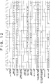
- a data processing unit according to a sixth embodiment of the present invention will be described with reference to Figures 11 to 13.
- FIG 11 is a block diagram showing the configuration of the data processing unit according to the sixth embodiment of the present invention.
- reference character 1b is a control unit
- 7a is a number-of-retrievals counter
- 14 is an output signal of the number-of-retrievals counter 7a
- 18a is a number-of-matches data signal carried in the execution data signal
- 18b is a nonmatching data signal
- 20a is a third data register as a 6-bit retrieval count number setting register
- 22 is a retrieval count number setting signal
- 23 is an output signal of the third data register 20a
- 25 is an adder
- 26 is an output signal of the adder
- 27 is a selector
- 28 is an output signal of the selector 27, and 29 is a selection signal for the selector 27.
- the execution unit 2, first memory 3, second memory 4, first data register 5, and second data register 6 are essentially the same in configuration as the corresponding elements in the fifth embodiment shown in Figure 9. Differences from the fifth embodiment are that the control unit 1b takes as inputs the output signal 14 of the search number counter 7a and the number-of-matches data signal 18a, that the control unit 1b additionally outputs the selection signal 29, that the bit count of the third data register 20a as a retrieval count number setting register is 6, that the output signal 23 of the third data register 20a is loaded into the number-of-retrievals counter 7a configured as a down counter, and that the adder 25 and selector 27 are additionally provided.
- FIG. 12 is a diagram showing operating waveforms of the data processing unit according to the sixth embodiment of the present invention
- Figure 13 is a diagram showing the contents of the second memory 4 at the completion of writing, wherein reference character 1z indicates the memory address (in decimal), 2z the memory data, 3z the number of matches, and 4z the end flag.
- the memory data 2z is the data written without being shifted in the arithmetic unit of Figure 1
- the number of matches, 3z is the data written after being shifted in the arithmetic unit of Figure 1.
- the position of the memory data 2z may be interchanged with the position of the number of matches, 3z, depending on how the shifter in the arithmetic unit is set up.
- Waveform 1w in Figure 12 will be used as the operating clock (CLK) of the data processing unit of Figure 11, and the data processing unit of Figure 11 will be described as operating in synchronism with the rising edge of the operating clock 1w.
- the control unit 1b sets the instruction execution signal 8 (waveform 2w in Figure 12) to the H level to execute the comparison instruction.
- the control unit 1b outputs the memory read control signal 10 (waveform 3w in Figure 12), in response to which the memory data signal 15 at the specified address is read out and stored in the second data register 6 (waveform 4w in Figure 12).
- comparison reference data Prior to the execution of the comparison instruction, comparison reference data is set in the first data register 5 by using the comparison reference data setting signal 9 (waveform 5w in Figure 12; comparison reference data value is 0), and the retrieval count number (the initial value for the number of retrievals) is set in the third data register 20a by using the retrieval count number setting signal 22 (waveform 12w in Figure 12; retrieval count number is 63).
- the execution unit 2 compares the output signal 17 (waveform 4w in Figure 12) of the second data register 6 with the output signal 16 (waveform 5w in Figure 12) of the first data register 5 and, when they match, outputs the comparison signal 13 to the control unit 1b, thereby setting the memory write control signal 12 (waveform 6w in Figure 12), to be output from the control unit 1b, to the H level to inhibit writing to the second memory 4 and count the number of consecutive matches.
- the execution unit 2 When they do not match, on the other hand, the execution unit 2 writes its result signal (waveform 7w in Figure 12) as the execution data signal 18 (nonmatching data signal 18b and number-of-matches data signal 18a), together with the end flag signal 11 (waveform 9w in Figure 12), to the second memory 4 at the address (single address) specified by the memory write address signal (waveform 8w in Figure 12) carried in the memory write control signal 12.
- the control unit 1b sets the initial value of the number-of-retrievals counter 7a (the output value of the third data register 20a) by the instruction execution signal 8, and the counter 7a starts to count down; when the output signal 14 (waveform 10w in Figure 12) of the number-of-retrievals counter 7a becomes 0, the control unit 1b sets the instruction execution signal 8 to the L level to terminate the comparison instruction and, at the same time, sets the end flag signal 11 to the H level.
- the selection signal 29 (waveform 14w in Figure 12) is set to the H level, assuming that the data in the remaining retrieval range also match the comparison reference data, and when the low order 8 bits of the number-of-retrievals counter output signal 14 (10w in Figure 12) and the execution unit result signal are all 0s, the high order 6 bits of the two signals are added together by the adder 25, and its output data 26 (waveform 15w in Figure 12) is written to the second memory 4 instead of the number of matches, 18a, whereupon the comparison instruction is terminated and the end flag signal 11 is set to the H level.
- the memory address 1z corresponds to the waveform 8w in Figure 12
- the 8-bit memory data 2z in bit positions from 0 to 7 corresponds to the waveform 4w in Figure 12
- the 6-bit match count data (the number of matches) 3z in bit positions from 8 to 13 corresponds to the waveform 7w in Figure 12
- the end flag 4z in the 14th bit position corresponds to the waveform 9w in Figure 12.
- the data processing unit of the sixth embodiment is capable of executing the comparison instruction for any given value by setting desired comparison reference data in the first data register 5 functioning as a comparison reference data setting register, and can arbitrarily set the number of retrievals, to be performed within the comparison range, in the third data register 20a functioning as a retrieval count number setting register, so that the comparison instruction can be terminated after performing an arbitrary number of retrievals. Furthermore, when data matches occur consecutively, the comparison instruction can be terminated by assuming that the remaining data also match the comparison reference data, thus shortening the entire retrieval time. Since the end flag signal 11 is thus written to the second memory 4, the last written data can be detected by just reading out the data written to the second memory 4.
- the data processing unit is equally implementable if data from some other memory is input as the comparison reference data to the first data register 5.
- a data processing unit according to a seventh embodiment of the present invention will be described with reference to Figures 14 and 15.
- Figure 14 is a block diagram showing the configuration of the data processing unit according to the seventh embodiment of the present invention.
- reference character 1c is a control unit
- 30 is a fourth data register as a number-of-matches setting register
- 31 is a match detection circuit
- 32 is a number-of-consecutive-matches setting signal
- 33 is an output signal of the fourth data register 30, and 34 is a match detection signal.
- the execution unit 2 In the data processing unit of the seventh embodiment, the execution unit 2, first memory 3, second memory 4, first data register 5, second data register 6, third data register 20a, adder 25, and selector 27 are essentially the same in configuration as the corresponding elements in the sixth embodiment shown in Figure 11. Differences from the sixth embodiment are that the control unit 1c takes as an input the match detection signal 34 instead of the number-of-matches data signal 18a, that the control unit 1c additionally outputs the number-of-consecutive-matches setting signal 32, and that the fourth data register 30 as a number-of-matches setting register and the match detection circuit 31 are additionally provided.
- Figure 15 is a diagram showing operating waveforms of the data processing unit according to the seventh embodiment of the present invention.
- Waveform 1w in Figure 15 will be used as the operating clock (CLK) of the data processing unit of Figure 14, and the data processing unit of Figure 14 will be described as operating in synchronism with the rising edge of the operating clock 1w.
- the control unit 1c sets the instruction execution signal 8 (waveform 2w in Figure 15) to the H level to execute the comparison instruction.
- the control unit 1c outputs the memory read control signal 10 (waveform 3w in Figure 15), in response to which the memory data signal 15 at the specified address is read out and stored in the second data register 6 (waveform 4w in Figure 15).
- comparison reference data Prior to the execution of the comparison instruction, comparison reference data is set in the first data register 5 by using the comparison reference data setting signal 9 (waveform 5w in Figure 15; comparison reference data value is 0), the retrieval count number (the initial value for the number of retrievals) is set in the third data register 20a by using the retrieval count number setting signal 22 (waveform 12w in Figure 15; retrieval count number is 63), and the number of matches (waveform 16w; the number of matches is 7) is set in the fourth data register 30 by using the number-of-consecutive-matches setting signal 32.
- comparison reference data setting signal 9 waveform 5w in Figure 15; comparison reference data value is 0
- the retrieval count number the initial value for the number of retrievals
- the third data register 20a by using the retrieval count number setting signal 22 (waveform 12w in Figure 15; retrieval count number is 63)
- the number of matches (waveform 16w; the number of matches is 7) is set in the fourth data register 30 by using the number-of-
- the execution unit 2 compares the output signal 17 (waveform 4w in Figure 15) of the second data register 6 with the output signal 16 (waveform 5w in Figure 15) of the first data register 5 and, when they match, outputs the comparison signal 13 to the control unit 1c, thereby setting the memory write control signal 12 (waveform 6w in Figure 15), to be output from the control unit 1c, to the H level to inhibit writing to the second memory 4 and count the number of consecutive matches (waveform 7w in Figure 15).
- the execution unit 2 When they do not match, on the other hand, the execution unit 2 writes its result signal (waveform 7w in Figure 15) as the execution data signal 18 (nonmatching data signal 18b and number-of-matches data signal 18a), together with the end flag signal 11 (waveform 9w in Figure 15), to the second memory 4 at the address (single address) specified by the memory write address signal (waveform 8w in Figure 15) carried in the memory write control signal 12.
- the control unit 1c sets the initial value of the number-of-retrievals counter 7a (the output value of the third data register 20a) by the instruction execution signal 8, and the counter 7a starts to count down; when the output signal 14 of the number-of-retrievals counter 7a becomes 0, the control unit 1c sets the instruction execution signal 8 to the L level to terminate the comparison instruction and, at the same time, sets the end flag signal 11 to the H level; or, when the number of consecutive matches becomes equal to the value set in the fourth data register 30, and the match detection signal goes to the H level (waveform 17w in Figure 15; the value is 700 in the illustrated example), the selection signal 29 (waveform 14w in Figure 15) is set to the H level, assuming that the data in the remaining retrieval range also match the comparison reference data, and when the low order 8 bits of the output signal 14 of the number-of-retrievals counter 7a and the execution unit result signal are all 0s, the high order 6 bits of the two signals are added together by the adder 25, and its output
- the data processing unit of the seventh embodiment is capable of executing the comparison instruction for any given value by setting desired comparison reference data in the first data register 5 functioning as a comparison reference data setting register, and can arbitrarily set the number of retrievals, to be performed within the comparison range, in the third data register 20a functioning as a retrieval count number setting register, so that the comparison instruction can be terminated after performing an arbitrary number of retrievals. Furthermore, by presetting the desired number of matches in the fourth data register 30 functioning as a number-of-matches setting register, when data matches occur consecutively the preset number of times, the comparison instruction can be terminated by assuming that the remaining data also match the comparison reference data, thus shortening the entire retrieval time. Since the end flag signal 11 is thus written to the second memory 4, the last written data can be detected by just reading out the data written to the second memory 4.
- the data processing unit is equally implementable if data from some other memory is input as the comparison data to the first data register 5.
- the number of data matches that occurred consecutively is written to a memory together with nonmatching data, and data from the memory is read out to continuously perform subsequent data processing and detect, at the same time, the last data written to the memory.
- a desired value is set in a data register, and a comparison instruction is issued by which the value set in the register is compared with a value set in a second register, and the number of matches that occurred consecutively is output together with nonmatching data; upon the output of a retrieval counter reaching a predetermined value, the comparison instruction is terminated, whereupon the number of consecutive matches, the nonmatching data, and an end flag signal are written to the memory at the same address.
Landscapes
- Engineering & Computer Science (AREA)
- Theoretical Computer Science (AREA)
- General Physics & Mathematics (AREA)
- Physics & Mathematics (AREA)
- General Engineering & Computer Science (AREA)
- Mathematical Analysis (AREA)
- Pure & Applied Mathematics (AREA)
- Mathematical Optimization (AREA)
- Computational Mathematics (AREA)
- Executing Machine-Instructions (AREA)
- Compression, Expansion, Code Conversion, And Decoders (AREA)
- Debugging And Monitoring (AREA)
- Management, Administration, Business Operations System, And Electronic Commerce (AREA)
- Hardware Redundancy (AREA)
Priority Applications (1)
| Application Number | Priority Date | Filing Date | Title |
|---|---|---|---|
| EP05023307A EP1622097A3 (de) | 1997-12-02 | 1998-12-01 | Arithmetische Einheit und Datenverarbeitungseinheit |
Applications Claiming Priority (2)
| Application Number | Priority Date | Filing Date | Title |
|---|---|---|---|
| JP33141797 | 1997-12-02 | ||
| JP33141797 | 1997-12-02 |
Related Child Applications (1)
| Application Number | Title | Priority Date | Filing Date |
|---|---|---|---|
| EP05023307A Division EP1622097A3 (de) | 1997-12-02 | 1998-12-01 | Arithmetische Einheit und Datenverarbeitungseinheit |
Publications (3)
| Publication Number | Publication Date |
|---|---|
| EP0921462A2 true EP0921462A2 (de) | 1999-06-09 |
| EP0921462A3 EP0921462A3 (de) | 2000-03-01 |
| EP0921462B1 EP0921462B1 (de) | 2005-10-26 |
Family
ID=18243450
Family Applications (2)
| Application Number | Title | Priority Date | Filing Date |
|---|---|---|---|
| EP05023307A Withdrawn EP1622097A3 (de) | 1997-12-02 | 1998-12-01 | Arithmetische Einheit und Datenverarbeitungseinheit |
| EP98122838A Expired - Lifetime EP0921462B1 (de) | 1997-12-02 | 1998-12-01 | Arithmetische Einheit |
Family Applications Before (1)
| Application Number | Title | Priority Date | Filing Date |
|---|---|---|---|
| EP05023307A Withdrawn EP1622097A3 (de) | 1997-12-02 | 1998-12-01 | Arithmetische Einheit und Datenverarbeitungseinheit |
Country Status (7)
| Country | Link |
|---|---|
| US (2) | US6332152B1 (de) |
| EP (2) | EP1622097A3 (de) |
| KR (1) | KR100531926B1 (de) |
| CN (1) | CN1150449C (de) |
| CA (1) | CA2254753A1 (de) |
| DE (1) | DE69832026T2 (de) |
| TW (1) | TW405085B (de) |
Cited By (1)
| Publication number | Priority date | Publication date | Assignee | Title |
|---|---|---|---|---|
| WO2010080445A3 (en) * | 2009-01-12 | 2010-08-26 | Micron Technology, Inc. | Devices, systems, and methods for communicating pattern matching results of a parallel pattern search engine |
Families Citing this family (21)
| Publication number | Priority date | Publication date | Assignee | Title |
|---|---|---|---|---|
| JP3765931B2 (ja) * | 1998-10-15 | 2006-04-12 | 富士通株式会社 | バッファ制御方法及びバッファ制御装置 |
| TW522374B (en) * | 2000-08-08 | 2003-03-01 | Semiconductor Energy Lab | Electro-optical device and driving method of the same |
| US6992652B2 (en) * | 2000-08-08 | 2006-01-31 | Semiconductor Energy Laboratory Co., Ltd. | Liquid crystal display device and driving method thereof |
| TW518552B (en) * | 2000-08-18 | 2003-01-21 | Semiconductor Energy Lab | Liquid crystal display device, method of driving the same, and method of driving a portable information device having the liquid crystal display device |
| US6987496B2 (en) * | 2000-08-18 | 2006-01-17 | Semiconductor Energy Laboratory Co., Ltd. | Electronic device and method of driving the same |
| US7180496B2 (en) | 2000-08-18 | 2007-02-20 | Semiconductor Energy Laboratory Co., Ltd. | Liquid crystal display device and method of driving the same |
| TW514854B (en) * | 2000-08-23 | 2002-12-21 | Semiconductor Energy Lab | Portable information apparatus and method of driving the same |
| US7184014B2 (en) * | 2000-10-05 | 2007-02-27 | Semiconductor Energy Laboratory Co., Ltd. | Liquid crystal display device |
| US6747623B2 (en) * | 2001-02-09 | 2004-06-08 | Semiconductor Energy Laboratory Co., Ltd. | Liquid crystal display device and method of driving the same |
| TWI273539B (en) | 2001-11-29 | 2007-02-11 | Semiconductor Energy Lab | Display device and display system using the same |
| JP3913534B2 (ja) * | 2001-11-30 | 2007-05-09 | 株式会社半導体エネルギー研究所 | 表示装置及びこれを用いた表示システム |
| JP4067878B2 (ja) * | 2002-06-06 | 2008-03-26 | 株式会社半導体エネルギー研究所 | 発光装置及びそれを用いた電気器具 |
| US7231561B2 (en) * | 2002-07-17 | 2007-06-12 | Ltx Corporation | Apparatus and method for data pattern alignment |
| JP2006286084A (ja) * | 2005-03-31 | 2006-10-19 | Fujitsu Ltd | 符号器、復号器および符号化方法 |
| US8321489B2 (en) | 2006-09-15 | 2012-11-27 | National Semiconductor Corporation | Software reconfigurable digital phase lock loop architecture |
| US8120637B2 (en) * | 2006-09-20 | 2012-02-21 | Cisco Technology, Inc. | Virtual theater system for the home |
| EP2122632B1 (de) * | 2006-12-22 | 2014-06-25 | Sidense Corp. | Zweifunktions-datenregister |
| KR20080069778A (ko) * | 2007-01-24 | 2008-07-29 | 삼성전자주식회사 | 멀티칩 테스트를 위한 반도체 메모리 장치의 테스트 회로및 그의 테스트 방법 |
| JP4935619B2 (ja) * | 2007-10-23 | 2012-05-23 | ヤマハ株式会社 | デジタル信号処理装置 |
| KR20100126690A (ko) * | 2008-02-18 | 2010-12-02 | 샌드브리지 테크놀로지스, 인코포레이티드 | 널-종료 문자열 동작을 가속화하는 방법 |
| CN115495152A (zh) * | 2022-09-15 | 2022-12-20 | 北京后摩智能科技有限公司 | 变长输入的存内计算电路 |
Family Cites Families (17)
| Publication number | Priority date | Publication date | Assignee | Title |
|---|---|---|---|---|
| US3935379A (en) | 1974-05-09 | 1976-01-27 | General Dynamics Corporation | Method of and system for adaptive run length encoding of image representing digital information |
| JPS5984292A (ja) * | 1982-11-08 | 1984-05-15 | 富士通株式会社 | Crtデイスプレイ制御装置 |
| JPH0815263B2 (ja) * | 1986-12-12 | 1996-02-14 | 株式会社日立製作所 | データ圧縮復元方法 |
| DE3856175T2 (de) * | 1987-06-05 | 1998-12-17 | Mitsubishi Denki K.K., Tokio/Tokyo | Digitales Signalverarbeitungssystem in dem ein Prozessor unter Kontrolle eines Hosts auf zwei Befehlsspeicher zugreift |
| US4841299A (en) * | 1987-08-31 | 1989-06-20 | Digital Recording Research Limited Partnership | Method and apparatus for digital encoding and decoding |
| US5184229A (en) | 1988-12-09 | 1993-02-02 | Fuji Photo Film Co., Ltd. | Compression coding device and expansion decoding device for picture signal |
| JP2834837B2 (ja) * | 1990-03-30 | 1998-12-14 | 松下電工株式会社 | プログラマブルコントローラ |
| JPH04112319A (ja) | 1990-09-03 | 1992-04-14 | Matsushita Electric Ind Co Ltd | データ格納方法と先入れ先だし装置 |
| DE4129614C2 (de) * | 1990-09-07 | 2002-03-21 | Hitachi Ltd | System und Verfahren zur Datenverarbeitung |
| US6435737B1 (en) * | 1992-06-30 | 2002-08-20 | Discovision Associates | Data pipeline system and data encoding method |
| JPH0736739A (ja) | 1993-07-22 | 1995-02-07 | Toshiba Eng Co Ltd | データ処理装置 |
| US6016538A (en) * | 1993-11-30 | 2000-01-18 | Texas Instruments Incorporated | Method, apparatus and system forming the sum of data in plural equal sections of a single data word |
| US5479527A (en) | 1993-12-08 | 1995-12-26 | Industrial Technology Research Inst. | Variable length coding system |
| KR0152038B1 (ko) * | 1994-10-17 | 1998-10-15 | 김광호 | 상대 주소를 이용한 가변장 복호화 장치 |
| EP0721285B1 (de) * | 1995-01-09 | 2001-04-18 | Matsushita Electric Industrial Co., Ltd. | Digitale Kodierungsvorrichtung |
| US5710561A (en) * | 1996-01-02 | 1998-01-20 | Peerless Systems Corporation | Method and apparatus for double run-length encoding of binary data |
| US6263420B1 (en) * | 1997-09-17 | 2001-07-17 | Sony Corporation | Digital signal processor particularly suited for decoding digital audio |
-
1998
- 1998-11-30 US US09/201,720 patent/US6332152B1/en not_active Expired - Fee Related
- 1998-12-01 CA CA002254753A patent/CA2254753A1/en not_active Abandoned
- 1998-12-01 DE DE69832026T patent/DE69832026T2/de not_active Expired - Fee Related
- 1998-12-01 EP EP05023307A patent/EP1622097A3/de not_active Withdrawn
- 1998-12-01 EP EP98122838A patent/EP0921462B1/de not_active Expired - Lifetime
- 1998-12-02 TW TW087119959A patent/TW405085B/zh not_active IP Right Cessation
- 1998-12-02 KR KR1019980052556A patent/KR100531926B1/ko not_active Expired - Fee Related
- 1998-12-02 CN CNB98122380XA patent/CN1150449C/zh not_active Expired - Fee Related
-
2001
- 2001-10-17 US US09/978,204 patent/US6564237B2/en not_active Expired - Fee Related
Cited By (2)
| Publication number | Priority date | Publication date | Assignee | Title |
|---|---|---|---|---|
| WO2010080445A3 (en) * | 2009-01-12 | 2010-08-26 | Micron Technology, Inc. | Devices, systems, and methods for communicating pattern matching results of a parallel pattern search engine |
| US8843523B2 (en) | 2009-01-12 | 2014-09-23 | Micron Technology, Inc. | Devices, systems, and methods for communicating pattern matching results of a parallel pattern search engine |
Also Published As
| Publication number | Publication date |
|---|---|
| US6564237B2 (en) | 2003-05-13 |
| US20020026466A1 (en) | 2002-02-28 |
| KR100531926B1 (ko) | 2006-06-20 |
| CN1150449C (zh) | 2004-05-19 |
| EP0921462A3 (de) | 2000-03-01 |
| US6332152B1 (en) | 2001-12-18 |
| EP1622097A3 (de) | 2007-03-07 |
| DE69832026D1 (de) | 2005-12-01 |
| CN1226697A (zh) | 1999-08-25 |
| TW405085B (en) | 2000-09-11 |
| EP0921462B1 (de) | 2005-10-26 |
| KR19990062729A (ko) | 1999-07-26 |
| DE69832026T2 (de) | 2006-07-13 |
| EP1622097A2 (de) | 2006-02-01 |
| CA2254753A1 (en) | 1999-06-02 |
Similar Documents
| Publication | Publication Date | Title |
|---|---|---|
| EP0921462A2 (de) | Arithmetische Einheit und Datenverarbeitungseinheit | |
| US6144322A (en) | Variable length code processor with encoding and/or decoding | |
| US7917733B2 (en) | Instruction code compression using instruction codes with reuse flags | |
| US5918252A (en) | Apparatus and method for generating a modulo address | |
| EP0702457A2 (de) | Verfahren und Apparat zur Komprimierung und Entkomprimierung von Daten | |
| US6915413B2 (en) | Micro-controller for reading out compressed instruction code and program memory for compressing instruction code and storing therein | |
| US7308553B2 (en) | Processor device capable of cross-boundary alignment of plural register data and the method thereof | |
| US5530662A (en) | Fixed point signal processor having block floating processing circuitry | |
| US6005502A (en) | Method for reducing the number of bits needed for the representation of constant values in a data processing device | |
| US5875323A (en) | Processor using implicit register addressing | |
| JP2971875B2 (ja) | 演算装置およびデータ処理装置 | |
| US5210713A (en) | Data storage method and first-in first-out memory device | |
| US20030126402A1 (en) | Device and method for information processing | |
| US20030056080A1 (en) | Register read circuit using the remainders of modulo of a register number by the number of register sub-banks | |
| JPH11163736A (ja) | プロセッサ | |
| JPS603715B2 (ja) | 可変長シフトレジスタ | |
| JP3293382B2 (ja) | データ圧縮装置及びデータ伸長装置 | |
| KR100199190B1 (ko) | 데이타 포착회로 | |
| JPS61201335A (ja) | プログラム格納方法 | |
| JPH07210449A (ja) | デュアルポートramアクセス回路 | |
| JPH06131150A (ja) | 符号化装置 | |
| JPS59218535A (ja) | 端末装置の処理方式 | |
| KR20000060415A (ko) | 헤드 스택 포인터 및 테일 스택 포인터를 구비한 스택 | |
| JPH04293120A (ja) | データソート回路 | |
| JPH05120005A (ja) | 前命令の繰り返し命令をもつプロセツサ |
Legal Events
| Date | Code | Title | Description |
|---|---|---|---|
| PUAI | Public reference made under article 153(3) epc to a published international application that has entered the european phase |
Free format text: ORIGINAL CODE: 0009012 |
|
| 17P | Request for examination filed |
Effective date: 19981201 |
|
| AK | Designated contracting states |
Kind code of ref document: A2 Designated state(s): DE FR GB |
|
| AX | Request for extension of the european patent |
Free format text: AL;LT;LV;MK;RO;SI |
|
| RIC1 | Information provided on ipc code assigned before grant |
Free format text: 6G 06F 7/02 A, 6G 06T 9/00 B, 6H 03M 7/46 B |
|
| PUAL | Search report despatched |
Free format text: ORIGINAL CODE: 0009013 |
|
| AK | Designated contracting states |
Kind code of ref document: A3 Designated state(s): AT BE CH CY DE DK ES FI FR GB GR IE IT LI LU MC NL PT SE |
|
| AX | Request for extension of the european patent |
Free format text: AL;LT;LV;MK;RO;SI |
|
| AKX | Designation fees paid |
Free format text: DE FR GB |
|
| 17Q | First examination report despatched |
Effective date: 20030224 |
|
| RTI1 | Title (correction) |
Free format text: ARITHMETIC UNIT |
|
| GRAP | Despatch of communication of intention to grant a patent |
Free format text: ORIGINAL CODE: EPIDOSNIGR1 |
|
| GRAP | Despatch of communication of intention to grant a patent |
Free format text: ORIGINAL CODE: EPIDOSNIGR1 |
|
| GRAS | Grant fee paid |
Free format text: ORIGINAL CODE: EPIDOSNIGR3 |
|
| GRAA | (expected) grant |
Free format text: ORIGINAL CODE: 0009210 |
|
| AK | Designated contracting states |
Kind code of ref document: B1 Designated state(s): DE FR GB |
|
| REG | Reference to a national code |
Ref country code: GB Ref legal event code: FG4D |
|
| REF | Corresponds to: |
Ref document number: 69832026 Country of ref document: DE Date of ref document: 20051201 Kind code of ref document: P |
|
| ET | Fr: translation filed | ||
| PLBE | No opposition filed within time limit |
Free format text: ORIGINAL CODE: 0009261 |
|
| STAA | Information on the status of an ep patent application or granted ep patent |
Free format text: STATUS: NO OPPOSITION FILED WITHIN TIME LIMIT |
|
| 26N | No opposition filed |
Effective date: 20060727 |
|
| PGFP | Annual fee paid to national office [announced via postgrant information from national office to epo] |
Ref country code: DE Payment date: 20061123 Year of fee payment: 9 |
|
| PGFP | Annual fee paid to national office [announced via postgrant information from national office to epo] |
Ref country code: GB Payment date: 20061129 Year of fee payment: 9 |
|
| PGFP | Annual fee paid to national office [announced via postgrant information from national office to epo] |
Ref country code: FR Payment date: 20061208 Year of fee payment: 9 |
|
| GBPC | Gb: european patent ceased through non-payment of renewal fee |
Effective date: 20071201 |
|
| PG25 | Lapsed in a contracting state [announced via postgrant information from national office to epo] |
Ref country code: DE Free format text: LAPSE BECAUSE OF NON-PAYMENT OF DUE FEES Effective date: 20080701 |
|
| REG | Reference to a national code |
Ref country code: FR Ref legal event code: ST Effective date: 20081020 |
|
| PG25 | Lapsed in a contracting state [announced via postgrant information from national office to epo] |
Ref country code: GB Free format text: LAPSE BECAUSE OF NON-PAYMENT OF DUE FEES Effective date: 20071201 |
|
| PG25 | Lapsed in a contracting state [announced via postgrant information from national office to epo] |
Ref country code: FR Free format text: LAPSE BECAUSE OF NON-PAYMENT OF DUE FEES Effective date: 20071231 |