EP0923138A2 - Dispositif semiconducteur à film mince, son procédé de fabrication et système d'affichage - Google Patents
Dispositif semiconducteur à film mince, son procédé de fabrication et système d'affichage Download PDFInfo
- Publication number
- EP0923138A2 EP0923138A2 EP99101740A EP99101740A EP0923138A2 EP 0923138 A2 EP0923138 A2 EP 0923138A2 EP 99101740 A EP99101740 A EP 99101740A EP 99101740 A EP99101740 A EP 99101740A EP 0923138 A2 EP0923138 A2 EP 0923138A2
- Authority
- EP
- European Patent Office
- Prior art keywords
- film
- thin
- impurity
- source
- ldd
- Prior art date
- Legal status (The legal status is an assumption and is not a legal conclusion. Google has not performed a legal analysis and makes no representation as to the accuracy of the status listed.)
- Granted
Links
Images






















Classifications
-
- H—ELECTRICITY
- H10—SEMICONDUCTOR DEVICES; ELECTRIC SOLID-STATE DEVICES NOT OTHERWISE PROVIDED FOR
- H10P—GENERIC PROCESSES OR APPARATUS FOR THE MANUFACTURE OR TREATMENT OF DEVICES COVERED BY CLASS H10
- H10P14/00—Formation of materials, e.g. in the shape of layers or pillars
- H10P14/20—Formation of materials, e.g. in the shape of layers or pillars of semiconductor materials
- H10P14/24—Formation of materials, e.g. in the shape of layers or pillars of semiconductor materials using chemical vapour deposition [CVD]
-
- G—PHYSICS
- G02—OPTICS
- G02F—OPTICAL DEVICES OR ARRANGEMENTS FOR THE CONTROL OF LIGHT BY MODIFICATION OF THE OPTICAL PROPERTIES OF THE MEDIA OF THE ELEMENTS INVOLVED THEREIN; NON-LINEAR OPTICS; FREQUENCY-CHANGING OF LIGHT; OPTICAL LOGIC ELEMENTS; OPTICAL ANALOGUE/DIGITAL CONVERTERS
- G02F1/00—Devices or arrangements for the control of the intensity, colour, phase, polarisation or direction of light arriving from an independent light source, e.g. switching, gating or modulating; Non-linear optics
- G02F1/01—Devices or arrangements for the control of the intensity, colour, phase, polarisation or direction of light arriving from an independent light source, e.g. switching, gating or modulating; Non-linear optics for the control of the intensity, phase, polarisation or colour
- G02F1/13—Devices or arrangements for the control of the intensity, colour, phase, polarisation or direction of light arriving from an independent light source, e.g. switching, gating or modulating; Non-linear optics for the control of the intensity, phase, polarisation or colour based on liquid crystals, e.g. single liquid crystal display cells
- G02F1/133—Constructional arrangements; Operation of liquid crystal cells; Circuit arrangements
- G02F1/1333—Constructional arrangements; Manufacturing methods
- G02F1/1345—Conductors connecting electrodes to cell terminals
- G02F1/13454—Drivers integrated on the active matrix substrate
-
- G—PHYSICS
- G09—EDUCATION; CRYPTOGRAPHY; DISPLAY; ADVERTISING; SEALS
- G09G—ARRANGEMENTS OR CIRCUITS FOR CONTROL OF INDICATING DEVICES USING STATIC MEANS TO PRESENT VARIABLE INFORMATION
- G09G3/00—Control arrangements or circuits, of interest only in connection with visual indicators other than cathode-ray tubes
- G09G3/20—Control arrangements or circuits, of interest only in connection with visual indicators other than cathode-ray tubes for presentation of an assembly of a number of characters, e.g. a page, by composing the assembly by combination of individual elements arranged in a matrix no fixed position being assigned to or needed to be assigned to the individual characters or partial characters
- G09G3/2007—Display of intermediate tones
- G09G3/2011—Display of intermediate tones by amplitude modulation
-
- G—PHYSICS
- G09—EDUCATION; CRYPTOGRAPHY; DISPLAY; ADVERTISING; SEALS
- G09G—ARRANGEMENTS OR CIRCUITS FOR CONTROL OF INDICATING DEVICES USING STATIC MEANS TO PRESENT VARIABLE INFORMATION
- G09G3/00—Control arrangements or circuits, of interest only in connection with visual indicators other than cathode-ray tubes
- G09G3/20—Control arrangements or circuits, of interest only in connection with visual indicators other than cathode-ray tubes for presentation of an assembly of a number of characters, e.g. a page, by composing the assembly by combination of individual elements arranged in a matrix no fixed position being assigned to or needed to be assigned to the individual characters or partial characters
- G09G3/34—Control arrangements or circuits, of interest only in connection with visual indicators other than cathode-ray tubes for presentation of an assembly of a number of characters, e.g. a page, by composing the assembly by combination of individual elements arranged in a matrix no fixed position being assigned to or needed to be assigned to the individual characters or partial characters by control of light from an independent source
- G09G3/36—Control arrangements or circuits, of interest only in connection with visual indicators other than cathode-ray tubes for presentation of an assembly of a number of characters, e.g. a page, by composing the assembly by combination of individual elements arranged in a matrix no fixed position being assigned to or needed to be assigned to the individual characters or partial characters by control of light from an independent source using liquid crystals
- G09G3/3611—Control of matrices with row and column drivers
-
- G—PHYSICS
- G09—EDUCATION; CRYPTOGRAPHY; DISPLAY; ADVERTISING; SEALS
- G09G—ARRANGEMENTS OR CIRCUITS FOR CONTROL OF INDICATING DEVICES USING STATIC MEANS TO PRESENT VARIABLE INFORMATION
- G09G3/00—Control arrangements or circuits, of interest only in connection with visual indicators other than cathode-ray tubes
- G09G3/20—Control arrangements or circuits, of interest only in connection with visual indicators other than cathode-ray tubes for presentation of an assembly of a number of characters, e.g. a page, by composing the assembly by combination of individual elements arranged in a matrix no fixed position being assigned to or needed to be assigned to the individual characters or partial characters
- G09G3/34—Control arrangements or circuits, of interest only in connection with visual indicators other than cathode-ray tubes for presentation of an assembly of a number of characters, e.g. a page, by composing the assembly by combination of individual elements arranged in a matrix no fixed position being assigned to or needed to be assigned to the individual characters or partial characters by control of light from an independent source
- G09G3/36—Control arrangements or circuits, of interest only in connection with visual indicators other than cathode-ray tubes for presentation of an assembly of a number of characters, e.g. a page, by composing the assembly by combination of individual elements arranged in a matrix no fixed position being assigned to or needed to be assigned to the individual characters or partial characters by control of light from an independent source using liquid crystals
- G09G3/3611—Control of matrices with row and column drivers
- G09G3/3648—Control of matrices with row and column drivers using an active matrix
-
- G—PHYSICS
- G09—EDUCATION; CRYPTOGRAPHY; DISPLAY; ADVERTISING; SEALS
- G09G—ARRANGEMENTS OR CIRCUITS FOR CONTROL OF INDICATING DEVICES USING STATIC MEANS TO PRESENT VARIABLE INFORMATION
- G09G3/00—Control arrangements or circuits, of interest only in connection with visual indicators other than cathode-ray tubes
- G09G3/20—Control arrangements or circuits, of interest only in connection with visual indicators other than cathode-ray tubes for presentation of an assembly of a number of characters, e.g. a page, by composing the assembly by combination of individual elements arranged in a matrix no fixed position being assigned to or needed to be assigned to the individual characters or partial characters
- G09G3/34—Control arrangements or circuits, of interest only in connection with visual indicators other than cathode-ray tubes for presentation of an assembly of a number of characters, e.g. a page, by composing the assembly by combination of individual elements arranged in a matrix no fixed position being assigned to or needed to be assigned to the individual characters or partial characters by control of light from an independent source
- G09G3/36—Control arrangements or circuits, of interest only in connection with visual indicators other than cathode-ray tubes for presentation of an assembly of a number of characters, e.g. a page, by composing the assembly by combination of individual elements arranged in a matrix no fixed position being assigned to or needed to be assigned to the individual characters or partial characters by control of light from an independent source using liquid crystals
- G09G3/3611—Control of matrices with row and column drivers
- G09G3/3685—Details of drivers for data electrodes
- G09G3/3688—Details of drivers for data electrodes suitable for active matrices only
-
- H—ELECTRICITY
- H10—SEMICONDUCTOR DEVICES; ELECTRIC SOLID-STATE DEVICES NOT OTHERWISE PROVIDED FOR
- H10D—INORGANIC ELECTRIC SEMICONDUCTOR DEVICES
- H10D30/00—Field-effect transistors [FET]
- H10D30/01—Manufacture or treatment
- H10D30/021—Manufacture or treatment of FETs having insulated gates [IGFET]
- H10D30/031—Manufacture or treatment of FETs having insulated gates [IGFET] of thin-film transistors [TFT]
- H10D30/0312—Manufacture or treatment of FETs having insulated gates [IGFET] of thin-film transistors [TFT] characterised by the gate electrodes
- H10D30/0314—Manufacture or treatment of FETs having insulated gates [IGFET] of thin-film transistors [TFT] characterised by the gate electrodes of lateral top-gate TFTs comprising only a single gate
-
- H—ELECTRICITY
- H10—SEMICONDUCTOR DEVICES; ELECTRIC SOLID-STATE DEVICES NOT OTHERWISE PROVIDED FOR
- H10D—INORGANIC ELECTRIC SEMICONDUCTOR DEVICES
- H10D30/00—Field-effect transistors [FET]
- H10D30/01—Manufacture or treatment
- H10D30/021—Manufacture or treatment of FETs having insulated gates [IGFET]
- H10D30/031—Manufacture or treatment of FETs having insulated gates [IGFET] of thin-film transistors [TFT]
- H10D30/0321—Manufacture or treatment of FETs having insulated gates [IGFET] of thin-film transistors [TFT] comprising silicon, e.g. amorphous silicon or polysilicon
-
- H—ELECTRICITY
- H10—SEMICONDUCTOR DEVICES; ELECTRIC SOLID-STATE DEVICES NOT OTHERWISE PROVIDED FOR
- H10D—INORGANIC ELECTRIC SEMICONDUCTOR DEVICES
- H10D30/00—Field-effect transistors [FET]
- H10D30/60—Insulated-gate field-effect transistors [IGFET]
- H10D30/67—Thin-film transistors [TFT]
- H10D30/6704—Thin-film transistors [TFT] having supplementary regions or layers in the thin films or in the insulated bulk substrates for controlling properties of the device
- H10D30/6713—Thin-film transistors [TFT] having supplementary regions or layers in the thin films or in the insulated bulk substrates for controlling properties of the device characterised by the properties of the source or drain regions, e.g. compositions or sectional shapes
-
- H—ELECTRICITY
- H10—SEMICONDUCTOR DEVICES; ELECTRIC SOLID-STATE DEVICES NOT OTHERWISE PROVIDED FOR
- H10D—INORGANIC ELECTRIC SEMICONDUCTOR DEVICES
- H10D30/00—Field-effect transistors [FET]
- H10D30/60—Insulated-gate field-effect transistors [IGFET]
- H10D30/67—Thin-film transistors [TFT]
- H10D30/6704—Thin-film transistors [TFT] having supplementary regions or layers in the thin films or in the insulated bulk substrates for controlling properties of the device
- H10D30/6713—Thin-film transistors [TFT] having supplementary regions or layers in the thin films or in the insulated bulk substrates for controlling properties of the device characterised by the properties of the source or drain regions, e.g. compositions or sectional shapes
- H10D30/6715—Thin-film transistors [TFT] having supplementary regions or layers in the thin films or in the insulated bulk substrates for controlling properties of the device characterised by the properties of the source or drain regions, e.g. compositions or sectional shapes characterised by the doping profiles, e.g. having lightly-doped source or drain extensions
-
- H—ELECTRICITY
- H10—SEMICONDUCTOR DEVICES; ELECTRIC SOLID-STATE DEVICES NOT OTHERWISE PROVIDED FOR
- H10D—INORGANIC ELECTRIC SEMICONDUCTOR DEVICES
- H10D30/00—Field-effect transistors [FET]
- H10D30/60—Insulated-gate field-effect transistors [IGFET]
- H10D30/67—Thin-film transistors [TFT]
- H10D30/6704—Thin-film transistors [TFT] having supplementary regions or layers in the thin films or in the insulated bulk substrates for controlling properties of the device
- H10D30/6713—Thin-film transistors [TFT] having supplementary regions or layers in the thin films or in the insulated bulk substrates for controlling properties of the device characterised by the properties of the source or drain regions, e.g. compositions or sectional shapes
- H10D30/6715—Thin-film transistors [TFT] having supplementary regions or layers in the thin films or in the insulated bulk substrates for controlling properties of the device characterised by the properties of the source or drain regions, e.g. compositions or sectional shapes characterised by the doping profiles, e.g. having lightly-doped source or drain extensions
- H10D30/6719—Thin-film transistors [TFT] having supplementary regions or layers in the thin films or in the insulated bulk substrates for controlling properties of the device characterised by the properties of the source or drain regions, e.g. compositions or sectional shapes characterised by the doping profiles, e.g. having lightly-doped source or drain extensions having significant overlap between the lightly-doped drains and the gate electrodes, e.g. gate-overlapped LDD [GOLDD] TFTs
-
- H—ELECTRICITY
- H10—SEMICONDUCTOR DEVICES; ELECTRIC SOLID-STATE DEVICES NOT OTHERWISE PROVIDED FOR
- H10D—INORGANIC ELECTRIC SEMICONDUCTOR DEVICES
- H10D30/00—Field-effect transistors [FET]
- H10D30/60—Insulated-gate field-effect transistors [IGFET]
- H10D30/67—Thin-film transistors [TFT]
- H10D30/6729—Thin-film transistors [TFT] characterised by the electrodes
- H10D30/673—Thin-film transistors [TFT] characterised by the electrodes characterised by the shapes, relative sizes or dispositions of the gate electrodes
- H10D30/6731—Top-gate only TFTs
-
- H—ELECTRICITY
- H10—SEMICONDUCTOR DEVICES; ELECTRIC SOLID-STATE DEVICES NOT OTHERWISE PROVIDED FOR
- H10D—INORGANIC ELECTRIC SEMICONDUCTOR DEVICES
- H10D30/00—Field-effect transistors [FET]
- H10D30/60—Insulated-gate field-effect transistors [IGFET]
- H10D30/67—Thin-film transistors [TFT]
- H10D30/674—Thin-film transistors [TFT] characterised by the active materials
- H10D30/6741—Group IV materials, e.g. germanium or silicon carbide
- H10D30/6743—Silicon
- H10D30/6745—Polycrystalline or microcrystalline silicon
-
- H—ELECTRICITY
- H10—SEMICONDUCTOR DEVICES; ELECTRIC SOLID-STATE DEVICES NOT OTHERWISE PROVIDED FOR
- H10D—INORGANIC ELECTRIC SEMICONDUCTOR DEVICES
- H10D86/00—Integrated devices formed in or on insulating or conducting substrates, e.g. formed in silicon-on-insulator [SOI] substrates or on stainless steel or glass substrates
- H10D86/40—Integrated devices formed in or on insulating or conducting substrates, e.g. formed in silicon-on-insulator [SOI] substrates or on stainless steel or glass substrates characterised by multiple TFTs
-
- H—ELECTRICITY
- H10—SEMICONDUCTOR DEVICES; ELECTRIC SOLID-STATE DEVICES NOT OTHERWISE PROVIDED FOR
- H10D—INORGANIC ELECTRIC SEMICONDUCTOR DEVICES
- H10D86/00—Integrated devices formed in or on insulating or conducting substrates, e.g. formed in silicon-on-insulator [SOI] substrates or on stainless steel or glass substrates
- H10D86/40—Integrated devices formed in or on insulating or conducting substrates, e.g. formed in silicon-on-insulator [SOI] substrates or on stainless steel or glass substrates characterised by multiple TFTs
- H10D86/60—Integrated devices formed in or on insulating or conducting substrates, e.g. formed in silicon-on-insulator [SOI] substrates or on stainless steel or glass substrates characterised by multiple TFTs wherein the TFTs are in active matrices
-
- H—ELECTRICITY
- H10—SEMICONDUCTOR DEVICES; ELECTRIC SOLID-STATE DEVICES NOT OTHERWISE PROVIDED FOR
- H10P—GENERIC PROCESSES OR APPARATUS FOR THE MANUFACTURE OR TREATMENT OF DEVICES COVERED BY CLASS H10
- H10P14/00—Formation of materials, e.g. in the shape of layers or pillars
- H10P14/20—Formation of materials, e.g. in the shape of layers or pillars of semiconductor materials
- H10P14/29—Formation of materials, e.g. in the shape of layers or pillars of semiconductor materials characterised by the substrates
- H10P14/2901—Materials
- H10P14/2921—Materials being crystalline insulating materials
-
- H—ELECTRICITY
- H10—SEMICONDUCTOR DEVICES; ELECTRIC SOLID-STATE DEVICES NOT OTHERWISE PROVIDED FOR
- H10P—GENERIC PROCESSES OR APPARATUS FOR THE MANUFACTURE OR TREATMENT OF DEVICES COVERED BY CLASS H10
- H10P14/00—Formation of materials, e.g. in the shape of layers or pillars
- H10P14/20—Formation of materials, e.g. in the shape of layers or pillars of semiconductor materials
- H10P14/32—Formation of materials, e.g. in the shape of layers or pillars of semiconductor materials characterised by intermediate layers between substrates and deposited layers
- H10P14/3202—Materials thereof
- H10P14/3238—Materials thereof being insulating materials
-
- H—ELECTRICITY
- H10—SEMICONDUCTOR DEVICES; ELECTRIC SOLID-STATE DEVICES NOT OTHERWISE PROVIDED FOR
- H10P—GENERIC PROCESSES OR APPARATUS FOR THE MANUFACTURE OR TREATMENT OF DEVICES COVERED BY CLASS H10
- H10P14/00—Formation of materials, e.g. in the shape of layers or pillars
- H10P14/20—Formation of materials, e.g. in the shape of layers or pillars of semiconductor materials
- H10P14/34—Deposited materials, e.g. layers
- H10P14/3402—Deposited materials, e.g. layers characterised by the chemical composition
- H10P14/3404—Deposited materials, e.g. layers characterised by the chemical composition being Group IVA materials
- H10P14/3411—Silicon, silicon germanium or germanium
-
- G—PHYSICS
- G09—EDUCATION; CRYPTOGRAPHY; DISPLAY; ADVERTISING; SEALS
- G09G—ARRANGEMENTS OR CIRCUITS FOR CONTROL OF INDICATING DEVICES USING STATIC MEANS TO PRESENT VARIABLE INFORMATION
- G09G2310/00—Command of the display device
- G09G2310/02—Addressing, scanning or driving the display screen or processing steps related thereto
- G09G2310/0264—Details of driving circuits
- G09G2310/027—Details of drivers for data electrodes, the drivers handling digital grey scale data, e.g. use of D/A converters
-
- G—PHYSICS
- G09—EDUCATION; CRYPTOGRAPHY; DISPLAY; ADVERTISING; SEALS
- G09G—ARRANGEMENTS OR CIRCUITS FOR CONTROL OF INDICATING DEVICES USING STATIC MEANS TO PRESENT VARIABLE INFORMATION
- G09G2310/00—Command of the display device
- G09G2310/02—Addressing, scanning or driving the display screen or processing steps related thereto
- G09G2310/0264—Details of driving circuits
- G09G2310/0283—Arrangement of drivers for different directions of scanning
-
- G—PHYSICS
- G09—EDUCATION; CRYPTOGRAPHY; DISPLAY; ADVERTISING; SEALS
- G09G—ARRANGEMENTS OR CIRCUITS FOR CONTROL OF INDICATING DEVICES USING STATIC MEANS TO PRESENT VARIABLE INFORMATION
- G09G2310/00—Command of the display device
- G09G2310/02—Addressing, scanning or driving the display screen or processing steps related thereto
- G09G2310/0264—Details of driving circuits
- G09G2310/0289—Details of voltage level shifters arranged for use in a driving circuit
-
- G—PHYSICS
- G09—EDUCATION; CRYPTOGRAPHY; DISPLAY; ADVERTISING; SEALS
- G09G—ARRANGEMENTS OR CIRCUITS FOR CONTROL OF INDICATING DEVICES USING STATIC MEANS TO PRESENT VARIABLE INFORMATION
- G09G2320/00—Control of display operating conditions
- G09G2320/02—Improving the quality of display appearance
- G09G2320/028—Improving the quality of display appearance by changing the viewing angle properties, e.g. widening the viewing angle, adapting the viewing angle to the view direction
-
- G—PHYSICS
- G09—EDUCATION; CRYPTOGRAPHY; DISPLAY; ADVERTISING; SEALS
- G09G—ARRANGEMENTS OR CIRCUITS FOR CONTROL OF INDICATING DEVICES USING STATIC MEANS TO PRESENT VARIABLE INFORMATION
- G09G2330/00—Aspects of power supply; Aspects of display protection and defect management
- G09G2330/02—Details of power systems and of start or stop of display operation
- G09G2330/021—Power management, e.g. power saving
Definitions
- the present invention relates to a thin-film semiconductor device comprising a non-single-crystal semiconductor film, a method of fabricating such a thin-film semiconductor device, and a display system in which this thin-film semiconductor device is used.
- Thin-film semiconductor devices that comprise non-single-crystal semiconductor films (including polycrystalline and amorphous semiconductor films) have recently come to be used in the display portions and peripheral circuitry of active matrix liquid crystal display devices. They are also used in image sensors and SRAM devices.
- thin-film semiconductor device is a generic term that could refer to a semiconductor film in itself, a thin-film transistor (TFT), or a CMOS type of TFT having a p-channel TFT and an n-channel TFT. In this document, it is sometimes referred to as a "thin-film semiconductor device” and sometimes simply as "TFT,” as required.
- peripheral circuitry such as that of a liquid crystal display device
- they are required to operate at high speed. If the operation speed of the thin film semiconductor devices is high enough to use them as the peripheral circuitry, they work as the switching thin-film semiconductor devices of the display portion and all the peripheral circuitry such as shift registers and analog switches can be simultaneously integrated onto the liquid crystal substrate with them.
- thin-film semiconductor devices may be used in digital and analog circuits where only single-crystal MOSFETs are used in the prior art.
- a thin-film semiconductor device differs from a single-crystal MOSFET in that it is formed on an insulating substance. This means that it is not affected by the problems with the single-crystal MOSFET, such as noise being transmitted through the substrate or latch-up being caused by current flowing through the substrate. This also means that increasing the speed of a thin-film semiconductor device is a technical objective.
- FIG. 56A An example of the configuration of such a thin-film semiconductor device is shown in Fig. 56A, with an equivalent circuit diagram of this thin-film semiconductor device being shown in Fig. 56B.
- Rc1 and Rc2 denote the contact resistances of a contact portion 412 (a contact between wiring 408 and a source portion 404) and a contact portion 414 (a contact between wiring 410 and a drain portion 406).
- Rs is the source resistance of the source portion 404
- Rch is the channel resistance of a channel portion 402
- Rd is the drain resistance of the drain portion 406.
- both the on-state channel resistance Rch(on) and the overall parasitic resistance Rp are reduced.
- Rch(on) it is necessary to find new fabrication methods of the semiconductor films which form the thin-film semiconductor device. More specifically, it would be advantageous to increase the carrier mobility of the semiconductor films and it would also be effective to shorten the channel portion 402.
- the resistances Rs and Rd may be reduced by either increasing the impurity concentration of the source portion and the drain portion, or improving the quality of the semiconductor films forming the source and drain portions.
- Rc1 and Rc2 it is possible to put barrier metal at the contact portion. It is, however, more effective to simply increase the impurity concentration of the source and drain portions rather than putting barrier metal, in view of simplifying the fabrication process.
- a polycrystalline silicon thin-film semiconductor device generally has carrier mobility of at least approximately 10 cm 2 /V.s, which is far higher than that of an amorphous silicon thin-film semiconductor device.
- a polycrystalline silicon film is first deposited by a low-pressure chemical vapor deposition (LPCVD) method at a deposition temperature of approximately 600°C or more.
- the size of the regions (islands) of which the polycrystalline silicon is composed ranges approximately from 20 nm to 80 nm.
- the polycrystalline silicon film surface is then thermally oxidized to form the semiconductor layer and gate insulation layer of the thin-film semiconductor device.
- the boundary surface roughness (center line average height, Ra) between the gate insulation film and gate electrode in this case is at least approximately 3.1 nm.
- One example of an n-channel type thin-film transistor made through this fabrication method has the carrier mobility of approximately 10 cm 2 /V.s to 20 cm 2 /V.s.
- the average grain area (average area of the grains) of the semiconductor film is approximately 4,000 to 6,000 nm 2 .
- an amorphous silicon film is first formed by plasma-enhanced CVD (PECVD).
- PECVD plasma-enhanced CVD
- the amorphous silicon film is then annealed in a nitrogen atmosphere at the temperature of 600 °C for about from 20 hours to 80 hours.
- This annealing process converts the amorphous silicon film into a polycrystalline silicon film (solid-phase crystallization method).
- the surface of this polycrystalline silicon film is thermally oxidized to form a semiconductor layer and gate insulation layer of the thin-film semiconductor device.
- the thin-film semiconductor device is structured, it is finally applied by a hydrogen plasma.
- an n-channel type thin-film transistor has the carrier mobility of approximately 150 cm 2 /V.s (refer to S. Takenaka, et al., Jpn. J. Appl. Phys. 29 , L2380 (1990)).
- a polycrystalline silicon film is first deposited by LPCVD at a deposition temperature of 610°C.
- Si + is implanted into this polycrystalline silicon film at a dose of approximately 1.5 ⁇ 10 15 cm -2 , which converts the polycrystalline silicon film into an amorphous film.
- the film is then annealed at 600°C in a nitrogen atmosphere for several tens of hours to several hundreds of hours, so that the amorphous silicon recrystallizes to obtain a polycrystalline silicon film.
- the surface of this polycrystalline silicon film is then thermally oxidized to form a semiconductor layer and gate insulation layer of the thin-film semiconductor device.
- a hydrogenated silicon nitride (p-Si N:H) film is deposited by PECVD over the device, and then the device is annealed in a furnace at 400°C to hydrogenate the device.
- p-Si N:H hydrogenated silicon nitride
- an n-channel type thin-film transistor has the carrier mobility of approximately 100 cm 2 /V.s (refer to T. Noguchi, et al., J. Electrochemical Soc., 134 , page 1771 (1987)).
- the second fabrication method which involves several tens of hours of furnace annealing after the amorphous silicon film is deposited, can provide a thin-film semiconductor device with high carrier mobility. This process is, however, remarkably long and causes serious fall in the productivity.
- the initial semiconductor film is deposited by PECVD in this second fabrication method, very many particles are generated in the reaction chamber. These particles cause many defects of the devices, because they fall on the substrate during the deposition. Therefore, the yield is very poor.
- the third fabrication method which involves the implantation of silicon atoms after the polycrystalline silicon film has been deposited and requires even longer furnace annealing, has an even longer and more complicated process than the above second fabrication method. If the process increases by even one step, that alone is sufficient to reduce the product yield. The need for several tens of hours to several hundreds of hours of furnace annealing is unrealistic from the mass-production point of view, and is thus not practicable.
- the first fabrication method which involves simple method of depositing a polycrystalline silicon film by LPCVD then the formation of a thin-film semiconductor device by thermal oxidation, is extremely useful from the points of view of mass production and stability, with an extremely simple process.
- the first fabrication method has problems in that the average grain area of the polycrystalline silicon produced by this method is small at approximately 4,000 to 6,000 nm 2 , and the carrier mobility is as low as at 10 cm 2 /V.s to 20 cm 2 /V.s.
- TFTs include a TFT of an ordinary structure and a lightly doped drain (hereinafter abbreviated to LDD) type of TFT.
- LDD lightly doped drain
- the present inventors consider that it is most preferable to use an LDD-type TFT.
- a gate insulation film 25 is first formed on thin semiconductor films 22 that have been patterned into islands on an insulating substrate 21, and gate electrodes 26 are formed thereover.
- impurity ions that work as donors in the semiconductor films are implanted at high concentration into the thin semiconductor film which will be the source and drain regions of the n-channel TFT, to form thin n + semiconductor films 23.
- impurity ions that work as acceptor in the semiconductor film are implanted at high concentration into the thin semiconductor film, which will be the source and drain regions of the p-channel TFT, to form thin p + semiconductor films 24.
- the resultant TFT is called a self-aligned TFT.
- a non-self-aligned TFT could equally well be produced by the first formation of thin n + semiconductor islands and thin p + semiconductor islands, containing appropriate impurities. These TFTs are covered with interlayer insulation film 27, and then wiring is patterned of thin metal films 28 to complete the TFTs of an ordinary structure.
- Single-crystal MOSFETs possessing LDD structure are widely used in semiconductor integrated circuits which are made on single-crystal substrates.
- the MOSFETs with LDD structure can restrain the device from generating hot carriers and can also increase its reliability.
- the prior art techniques of LDD-type MOSFETs are described in, for example, Japanese Patent Application Laid-Open Nos. 2-58274 and 2-45972.
- Prior art fabrication methods for LDD-type MOSFETs are described in, for example, Japanese Patent Application Laid-Open Nos. 62-241375 and 62-234372. Since the diffusion coefficient of the impurities in the single-crystal semiconductor material is low, the LDD length can be shorten to approximately one-tenth of the channel length.
- the source-drain current of the transistor on-state (ON-current) of an LDD-type MOSFET is reduced to only about one-tenth of that of an ordinary-structure MOSFET.
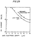
- the impurity ions acceleratingly diffuse along the grain boundaries of the semiconductor films. This means the actual diffusion coefficient in poly-Si films increases with the amount of at least one order of magnitude over that in the single-crystal semiconductor. Therefore, the LDD length of the LDD-type TFT should be long, and the high electric resistance of this LDD portion causes a problem in that the ON current becomes one-half or less than that of a TFT of an ordinary structure. That is why the prior art LDD-type TFT has not been used in circuits that are required to operate at high speeds.
- the effective n-channel channel length Leffn and the effective p-channel channel length Leffp are the lengths obtained by subtracting twice the corresponding overlapping portion Yjn or Yjp from the n-channel gate electrode length (see Fig. 27; note that this is sometimes called the gate electrode width) Lgaten or the p-channel gate electrode length Lgatep.
- a gate electrode length of at least 6 ⁇ m is required because these overlapping portions are at least 1 ⁇ m long.
- the impurity dose implanted into the LDD region by this prior art technique should be 1 ⁇ 10 14 cm -2 or less (refer to lines 45 to 48 of the left column of page 5).
- this numerical limit is not intended for optimizing the ON/OFF current ratio; it is nothing more than a numerical limit for simply reducing the OFF current and restraining leakage currents. Therefore, the ON current cannot be increased with the above limit even though the OFF current can be reduced. This is because, as the impurity dose implanted into the LDD region becomes smaller, the resistance of this LDD region increases and the ON current decreases.
- the impurity dose implanted into the source and drain portions is disclosed to be in the range of between 1 ⁇ 10 14 and 1 ⁇ 10 17 cm - 2 (refer to lines 11 to 14 of the right column of page 5).
- this numerical limit is neither intended for optimizing the diffusion length due to accelerated diffusion, nor reducing the resistances Rc, Rs, and Rd.
- the description of this prior art technique concerns a channel length that is set to 6 ⁇ m; it discloses nothing about a technique of reducing the channel length of a TFT by making the channel length 5 ⁇ m or less.
- the present invention is designed with the intention of solving the above described technical problems, and has an objective thereof the provision of a thin-film semiconductor device which can be fabricated by a simple, effective process and which also has good characteristics.
- the present invention is also intended to provide a method of fabricating such a thin-film semiconductor device and a display device using this thin-film semiconductor device.
- Another objective of the present invention is to provide an LDD-type thin-film semiconductor device that is capable of operating at high speed without requiring the addition of any novel processing steps.
- the present invention is also intended to provide a method of fabricating such a thin-film semiconductor device and a display device using this thin-film semiconductor device.
- a further objective of the present invention is to implement higher speeds for thin-film semiconductor devices, and provide a thin-film semiconductor device that can be used in the digital and analog circuits that used single-crystal MOSFETs in the prior art, thus broadening the field of application of such thin-film semiconductor devices, and a method of fabricating this thin-film semiconductor device.
- a first aspect of the present invention concerns a thin-film semiconductor device comprising a non-single-crystal semiconductor film formed on an insulating material portion which covers at least one portion of a surface of a substrate, wherein:
- the maximum impurity concentration of the first impurity-doped semiconductor film is optimized.
- diffusion of impurities from the source and drain portions into the LDD portion can be restrained and the breakdown voltage between the source and drain portions of the thin-film semiconductor device can be heightened by setting this maximum impurity concentration to be 1 ⁇ 10 21 cm -3 or less.
- both the contact resistance and the source and drain resistance can be reduced, that can result in the fast work of the thin-film semiconductor device by setting this maximum impurity concentration to be 5 ⁇ 10 19 cm -3 or more.
- the maximum impurity concentration it is preferable to set the maximum impurity concentration to be in the range of between 1 ⁇ 10 20 cm -3 and 3 ⁇ 10 20 cm -3 , since this enables the implementation of faster operation of the devices and even further miniaturization of components, while making the breakdown voltage high.
- a second aspect of the present invention concerns a thin-film semiconductor device comprising a non-single-crystal semiconductor film formed on an insulating material portion which covers at least one portion of a surface of a substrate, wherein:
- the present invention implements miniaturization of components by setting the LDD length to be 4 ⁇ m or less. Setting the LDD length to 0.6 ⁇ m or more would prevent the effective LDD length from disappearing, which is caused from the diffusion of impurities from the source and drain portions, thus prevents further any lowering of the breakdown voltage. In this case, to achieve further optimization, it is preferable that this LDD length is in the range of between 1 ⁇ m and 2 ⁇ m.
- a third aspect of the present invention concerns a thin-film semiconductor device comprising a non-single-crystal semiconductor film formed on an insulating material portion which covers at least one portion of a surface of a substrate, wherein:
- the channel can be decreased in length as the gate electrode length is set to 5 ⁇ m or less, so that some reduction in the ON current caused by the use of the LDD structure can be sufficiently compensated for, thus enabling faster operation of the devices.
- the gate electrode length is preferably 3 ⁇ m or less. This is not only because such a short channel length can further increase the operation speed of the device, but also because the supply voltage to the device can be reduced.
- a fourth aspect of the present invention concerns a thin-film semiconductor device comprising a non-single-crystal semiconductor film formed on an insulating material portion which covers at least one portion of a surface of a substrate, wherein:
- Lcontd can be set to a range of ⁇ 20% of Llddd. This makes it possible to prevent any excessive increase in the contact resistance, and also to reduce the parasitic resistance based on factors such as the resistance of the LDD portion.
- a fifth aspect of the present invention concerns a p-type thin-film transistor having first and second impurity-doped semiconductor films in which the implanted impurities are p-type and an n-type thin-film transistor having first and second impurity-doped semiconductor films in which the implanted impurities are n-type.
- This CMOS configuration enables an apparatus that is faster but consumes less power, so that it can provide the optimum thin-film semiconductor device for use in the peripheral circuitry of a liquid crystal display device, for example.
- the gate electrode length of the p-type thin-film transistor is preferably shorter than the gate electrode length of the n-type thin-film transistor. This enables a balance between the ON currents of the p-type and n-type thin-film transistors, and also, because circuits can be configured with the same channel width, the implementation of high-density circuits.
- the channel width of the n-type thin-film transistor is smaller than the channel width of the p-type thin-film transistor. This enables an even further increase in speed because of balancing the ON currents. If, for example, all the gate electrode lengths could be set to the minimum dimensions of the design rules, management of the fabrication process would become easier.
- the gate electrode length of the p-type thin-film transistor and the gate electrode length of the n-type thin-film transistor are each preferably 5 ⁇ m or less, because this implements a further increase in speed of the TFTs.
- a sixth aspect of the present invention concerns a method of fabricating a thin-film semiconductor device comprising a non-single-crystal semiconductor film formed on an insulating material portion which covers at least one portion of a surface of a substrate, comprising the steps of:
- impurities can be implanted at a low energy but with a high throughput.
- the LDD length can be freely set, so that the LDD structure can be formed only as necessary in required areas, thus increasing the degree of freedom of circuit design. Optimization of the implanted impurities is also facilitated.
- the sequence could be such that an impurity is at first implanted using the gate electrode as a mask, secondly an insulation film is formed on the surface of the gate electrode, and finally an impurity is again implanted to the semiconductor film.
- the method in accordance with this aspect of the present invention further comprises a step of forming an impurity-doped semiconductor film in the shape of an island shape in source and drain portions of a thin-film transistor, then forming an intrinsic semiconductor film on the impurity-doped semiconductor film formed in the shape of an island.
- an insulation film formed on the gate electrode surface layer portion could be formed by thermal oxidation or anodic oxidation of the material of the gate electrode, or by some deposition methods.
- a deposition method such as a chemical vapour deposition method forms an insulation film at a low temperature with a high throughput. Suitable combinations of these methods could be used to form a multi-layer insulation film, which would enable a further reduction in defects.
- An seventh aspect of the present invention concerns a display system using a thin-film semiconductor device comprising a non-single-crystal semiconductor film formed on an insulating material portion which covers at least one portion of a surface of a substrate, wherein:
- the maximum impurity concentration of the first impurity-doped semiconductor film and/or LDD length can be optimized by the present invention, to enable a further reduction in the length of the channel.
- the data driver portion or the scan driver portion may comprise a clocked gate bidirectional shift register circuit. This enables a simple method of reversing a screen image either horizontally or vertically, thus broadening the range of applications of the display device.
- the data driver portion or the scan driver portion may comprise a plurality of shift register circuits each of which has a different clock signal phase, and gate-circuits to which outputs from the plurality of shift register circuits are input.
- This enables the generation of various different timing pulses at high speed. For example, it enables the serial input of data driver signals for the Japanese high-definition television (HDTV) system, which is impossible in the prior art.
- HDTV Japanese high-definition television
- the data driver portion or the scan driver portion may comprise a level-shifter circuit and a shift register circuit, where the shift register circuit is driven at or below the TTL level. This ensures that the entire interface for external signals operates at or below the TTL level, enabling the implementation of smaller, less expensive, less power-consuming external circuits.
- an input portion of the level-shifter circuit may comprise a p-type thin-film transistor and an n-type thin-film transistor connected in series. This enables stable operation even when the difference between input and output voltages is large.
- the data driver portion comprises at least one shift register circuit, at least one video line, and analog switches; and one of outputs of the shift register circuit is input to a gate terminal of the analog switch, either directly or through a level-shifter circuit; whereby an analog signal is supplied to each of picture elements in a dot-sequential manner.
- the data driver portion comprises first-stage analog latches, each of which is connected to at least one video line, second-stage analog latches, each of which has at least one input to which an output from the first-stage analog latch enters, and analog buffers, each of which is connected to one of signal lines to which outputs from the second-stage analog latches are input; whereby an analog signal is supplied to each of picture elements in a line-sequential manner.
- the data driver portion comprises a group of n first-stage latches connected to n digital signal input lines, a group of n second-stage latches to which outputs of the first-stage latches are input, and a decoder connected to 2 n analog switch gates to which outputs of the second-stage latches are input; whereby digital signals are supplied to picture elements.
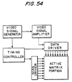
- the display system further comprises a video signal amplification circuit for amplifying video signals output from a video signal generator and a timing controller for generating timing signals in synchronization with video signals output from the video signal generator, wherein the data driver portion and the scan driver portion are driven by the timing signals.
- the timing controller, the data driver portion, and the scan driver portion are driven at levels equal to or below the TTL level. This makes the external circuits extremely simple.
- the timing controller is made from the thin-film semiconductor device. This enables a system that is even more compact and inexpensive.
- the video signal amplification circuit comprises a signal frequency conversion circuit for converting a video signal into a plurality of low-frequency signals or a gamma correction circuit. This improves the horizontal resolution and also increase grayscale levels.
- the video signal amplification circuit is made from the thin-film semiconductor device.
- the video signal amplification circuit is formed integrally of the thin-film semiconductor device of the present invention in this manner, the display system can be made much more compact and inexpensive.
- a twentieth aspect of the present invention concerns a thin-film semiconductor device comprising a non-single-crystal semiconductor film formed on an insulating material portion which covers at least one portion of a surface of a substrate, wherein:
- the semiconductor film is formed under the principle that the nucleus generation rate is retarded and the island growth rate is accelerated, thus enabling the implementation of an LDD-type TFT circuit comprising this semiconductor film.
- This has further advantages such as enabling an increase in carrier mobility, a reduction in contact resistance and in the channel length of the transistor, and an increase in the breakdown voltage, thus enabling the implementation of a high-speed thin-film semiconductor device that is not inferior to a single-crystal MOSFET.
- the island regions forming the semiconductor film in accordance with the present invention are extremely large, the resultant polycrystalline configuration after annealing has an extremely low level of crystal defects. Therefore, the electric resistance of the LDD portion can be reduced and the ON current can be further improved.
- the maximum impurity concentration of the first and second impurity-doped semiconductor films and/or LDD length can be optimized by the present invention, to enable a further reduction in the length of the channel.
- the range of the maximum impurity concentration can be set in the range of between 2 ⁇ 10 17 cm -3 and 1 ⁇ 10 19 cm -3 , thus broadening the setting range of the maximum impurity concentration.
- the semiconductor film is formed under the principle of the present invention that the nucleus generation rate is retarded and the island growth rate is accelerated, the number of crystal defects is reduced and, thus, the electric resistance of the LDD portion can be lowered. Therefore, the sheet resistance of the LDD portion is still low, even if the maximum impurity concentration of the LDD portion is set low. This is why the lower limit of the maximum impurity concentration of the LDD portion can be set as low as 2 ⁇ 10 17 cm -3 .
- the LDD length can be set to be in the range of between 0.3 ⁇ m and 4 ⁇ m, thus enabling a broadening of the setting range of the LDD length.
- the semiconductor film since the semiconductor film is formed under the principle of the present invention that the nucleus generation rate is retarded and the island growth rate is accelerated, the semiconductor film has rather little grain boundary, restraining impurities from acceleratingly diffusing along the grain boundaries. Therefore, the minimum LDD length can be shortened to approximately 0.3 ⁇ m. This enables a further reduction in the parasitic resistance of the LDD portion.
- the second impurity-doped semiconductor film is arranged over the entire region of source and drain portions of a p-type thin-film transistor having an impurity-doped semiconductor film in which the implanted impurity is p-type.
- the sheet resistance of the second impurity-doped semiconductor film in which an impurity is implanted at low concentration in accordance with the present invention can be reduced.
- the step of implanting an impurity to high concentration in the p-type thin-film transistor can be omitted, and the entire region of the source and drain portions can be made from the low-concentration second impurity-doped semiconductor film. This enables reduction of one processing step, such as a photoprocessing step, and also makes it easier to increase the density of the integrated circuits.
- Figs. 1A to 1D The process of fabricating a thin-film semiconductor device according to a first embodiment of the present invention is shown in Figs. 1A to 1D. These figures illustrate the process of fabricating an n-channel TFT as an example, but the present invention can equally well be applied to the fabrication of a p-channel TFT or a CMOS type of TFT which consists of an n-channel TFT and a p-channel TFT (see Fig. 26). The present invention can also be applied to the TFT which has two gate electrodes.
- quartz glass is used as a substrate 201.
- any type or size of substrate could be used, provided the substrate is capable of withstanding the maximum temperature achieved within the process of fabricating the thin-film semiconductor device.
- a semiconductor film such as silicon that is to form the active layer is first deposited on the substrate 201.
- an underlying protective film such as a silicon dioxide film or silicon nitride film could be deposited before the semiconductor film is deposited (see Fig. 25).
- an intrinsic silicon film is deposited by LPCVD on the substrate 201.
- the thickness of the film after this deposition is 1000 ⁇ .
- the LPCVD apparatus is hot-wall type, having volume of 184.5 L.
- the total reactive area in the LPCVD chamber when substrates are set is approximately 44,000 cm 2 .
- the deposition temperature is 510°C, mono-silane (SiH 4 ) of purity of at least 99.99% is used as the reactant gas, and the gas is supplied to the reaction chamber at a flow rate of 100 sccm.
- the deposition pressure is 0.8 Torr and a silicon film is deposited under these conditions at a deposition rate of 21.5 ⁇ /minute.
- the thus-deposited silicon film is subjected to patterning to obtain a silicon film 202 (see Fig. 1A).
- the patterned silicon film 202 is then thermally oxidized to form a silicon dioxide film 203 on the surface of the silicon film 202.
- Thermal oxidation is performed for 23 minutes, 36 seconds at one atmospheric pressure in a 100% oxygen environment at 1160°C. This process thins the silicon film to 400 ⁇ , to obtain a silicon dioxide film with film thickness of 1200 ⁇ (see Fig. 1B).
- 11 B + ions are next implanted into the semiconductor film at a dose of 2 ⁇ 10 12 cm -2 with an acceleration voltage of 40 kV.
- a gate electrode 204 is then formed from a silicon film containing donors or acceptors.
- the gate electrode is formed of a 3500 ⁇ -thick layer of polycrystalline silicon containing phosphorus.
- the sheet resistance of the thus-obtained gate electrode is 25 ⁇ / ⁇ .
- the gate electrode is then used as a mask for the implantation of impurity ions 205 that will become donors or acceptors, so as to form source and drain portions 206 and a channel region 207 (see Fig. 1C).
- phosphorus is selected as the impurity ion, and this impurity is implanted at a dose of 2 ⁇ 10 15 cm -2 with an acceleration voltage of 90 kV.
- An interlayer insulation film 208 is next deposited by means such as an atmospheric pressure CVD method.
- This interlayer insulation film is formed of a silicon dioxide film with film thickness of 5000 ⁇ .
- furnace annealing is performed for 20 minutes in a nitrogen atmosphere at 1000°C to both anneal the interlayer insulation film and activate the impurity ions that have been added to the source and drain portions.
- Contact holes are then opened and wires 209 of a material such as aluminum are passed therethrough to complete the thin-film semiconductor device (see Fig. 1D).
- the transistor characteristics of the n-channel TFT of the thus-formed thin-film semiconductor device are measured, with the results being as shown in Fig. 2.
- the length and width of the channel are both 10 ⁇ m, and measured at room temperature.
- the source-drain voltage (Vds) is 4 V and the gate voltage (Vgs) is 10 V (under this condition, the transistor is in ON state)
- the source-drain current (lds) is 75.6 ⁇ A, as shown in Fig. 2.
- Vds is 4 V and Vgs is 0 V (under this condition, the transistor is in OFF state)
- lds is 0.203 pA.
- both the ON current and the OFF current will improve to the values of 102 ⁇ A and 0.0318 pA, respectively, under the same measurement condition as those described above.
- the resultant carrier mobility is 129 cm 2 /V.s.
- This first embodiment demonstrates that a high-performance thin-film semiconductor device can be fabricated in a simple manner, without requiring troublesome processing steps such as the implantation of silicon atoms or (re-)crystallization of the semiconductor film by lengthy furnace annealing, merely by using the deposition conditions of the present invention while the silicon film is being deposited by LPCVD.
- a variety of thin-film semiconductor devices were fabricated by the fabrication process described in the first embodiment, except that the deposition conditions of the silicon film that is to form the active layer were varied. Note, however, that no hydrogenation is performed in this second embodiment.
- silicon films were deposited under various conditions to investigate the relationship between transistor characteristics and deposition conditions.
- the silicon films are deposited by the LPCVD apparatus described in the section on the first embodiment.
- the reactant gas is mono-silane of purity of at least 99.99%.
- the deposition temperature for the silicon film is varied between 490°C and 650°C, the mono-silane flow rate for the deposition is varied in the range of between 10 sccm and 100 sccm, and the deposition pressure is set as appropriate in the range of between 1 m Torr and 0.8 Torr.
- various silicon films were deposited under differing deposition conditions.
- the film thickness of all the deposited silicon films was in 1000 ⁇ 50 ⁇ .
- the thin-film semiconductor devices were completed by exactly the same fabrication process as that of the first embodiment.
- the film thickness of all the silicon films after the thermal oxidation is 400 ⁇ 50 ⁇
- the film thickness of the silicon dioxide film that acts as the gate insulation film is 1200 ⁇ 50 ⁇ .
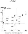
- Fig. 3 shows the relationships between the carrier mobility of each of the thin-film semiconductor devices obtained by the above described method and the deposition temperature and deposition rate of the silicon film.
- the horizontal axis of the Fig. 3 shows the silicon film deposition temperature while the vertical axis shows the deposition rate.
- the carrier mobilities of the corresponding thin-film semiconductor devices are expressed numerically in Fig. 3.
- the units of carrier mobility are cm 2 /V.s.
- the dotted lines in the figure show boundary lines indicating a deposition temperature of 580°C and a deposition rate of 6 ⁇ /minute.
- transistors having good electrical properties are indicated by circles in the figure, while transistors having nearly the same electrical properties as those of thin-film semiconductor devices produced as comparative examples (by the first fabrication method described in the section on the background of the invention) are indicated by crosses.
- the temperature for depositing directly the polycrystalline silicon films of the comparative examples is approximately 600°C or more. All of the thin-film semiconductor devices fabricated as comparative examples have carrier mobilities of between approximately 15 cm 2 /V.s and approximately 20 cm 2 /V.s.
- the silicon film deposition temperature is approximately 580°C or less
- the characteristics of thin-film semiconductor devices are strongly dependent on the deposition rate of the silicon films.
- the deposition rate is 6 ⁇ /minute or more
- the correspondent thin-film semiconductor devices have extremely good electrical characteristics, even without applying the hydrogenation process described in the section on the first embodiment.
- the carrier mobility ranges from approximately 16 cm 2 /V.s to approximately 19 cm 2 /V.s, which is about the same as the devices produced as comparative examples.
- An extremely high-performance thin-film semiconductor device can be obtained only when the thin-film semiconductor device is fabricated under conditions such that the deposition temperature is 580°C or less and the deposition rate is 6 ⁇ /minute or more.
- the silicon films forming the active layers of the thin-film semiconductor devices in accordance with the present invention are investigated by a scanning electron microscope (SEM). After the thermal oxidation, each silicon dioxide film is removed by a 10% aqueous solution of hydrogen fluoride, then the exposed polycrystalline silicon surface is observed by the SEM. SEM observation shows that the grain area distribute in accordance with an exponential distribution and both the average grain area and the standard deviation of the grain area are in the range of between 10,000 nm 2 and 20,000 nm 2 for all silicon films.
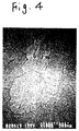
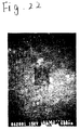
- Fig.4 shows a scanning electron microscope (SEM) photograph, as an example, of the crystal structure of the silicon film deposited at 510°C with the deposition rate of 12.9 ⁇ /minute, which has carrier mobility of 82 cm 2 /V.s. when it is used as the active layer of thin film transistors.
- the grain area distribution verified by Fig. 4 is shown in Fig. 6A.
- the average grain area (grain size) is 15,600 nm 2 with a standard deviation of 15,300 nm 2 .
- Each silicon film formed by the method in accordance with this embodiment contains large grains and some grains have their area of more than 55,000 nm 2 (see the range of 55,000 nm 2 to 60,000 nm 2 in Fig. 6A).
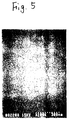
- Fig. 5 is a scanning electron microscope (SEM) photograph showing the crystal structure of a silicon film of a thin-film semiconductor device obtained as a comparative example (produced by the first fabrication method) as an example.
- the grain area distribution of this comparative example is shown in Fig. 6B.
- the testpiece used for Figs. 5 and 6B is deposited at a deposition temperature of 600°C and a deposition rate of 37.7 ⁇ /minute.
- Fig. 5 shows the state of the silicon film after thermal oxidation.
- the carrier mobility of this silicon film is 20 cm 2 /V.s.
- the average grain area of the film is 3,430 nm 2 , with a standard deviation of 4,210 nm 2 .
- Both the average and standard deviation of the grain size of a silicon film are always less than 5,000 nm 2 , either if the silicon film is deposited at the temperature of 600°C or more, or if the silicon film is deposited at the deposition rate of less than 6 ⁇ /minute.
- the films deposited at the temperature of 580°C or less with the deposition rate of less than 6 ⁇ /minute also consist of small grains such as less than 5,000 nm 2 .
- the average grain area of the polycrystalline film forming the active layer of transistor is at least 10,000 nm 2 , by far greater than that of the prior art, and the characteristics of the thin-film semiconductor device are also greatly improved.
- the present invention forms a semiconductor film with superior characteristics by depositing a semiconductor film under conditions such that the nucleus generation rate is retarded and the island growth rate is accelerated.
- the principle of the present invention is described below with reference to Figs. 7A to 7E and Figs. 8A to 8H.
- nuclei points which act as seeds or centers for film growth
- a number of nuclei points which act as seeds or centers for film growth
- a number of nuclei points which act as seeds or centers for film growth
- Fig. 7A Reactant molecules forming the reactant gas are transferred from the gaseous phase to the substrate. These molecules are subjected to heat from the substrate and undergo a chemical reaction, causing a number of these molecules to gather to form nuclei.
- the chemical reaction at this point taking mono-silane as an example, is as follows: SiH 4 ⁇ Si + 2H 2 ⁇
- nuclei 30 and 31 grow to become islands 34 and 35, and, at the same time, more nuclei 32 and 33 form in vacant regions on the substrate (Fig. 7B). These nuclei 32 and 33 also grow into islands 36 and 37, while the other islands 34 and 35 also grow further (Fig. 7C). As the vacant regions between islands disappear in this manner, no more new nuclei appear.
- the islands 34 to 37 continue to grow until they combine to form a thin film 38 (Fig. 7D). This thin film 38 grows further until a thin film 40 of preferred film thickness is complete (Fig. 7E). Fig.
- the thin film 40 is made up of regions (which will be called “islands” in the final stage of deposition process) 51, 52, 53, and 54 that correspond to the original islands formed in the initial stage of deposition process, regardless of whether the silicon film is amorphous or polycrystalline.
- Island growth and nucleus generation compete with each other up until the insulating substance surface is completely covered by the deposited film. Therefore, if the nucleus generation rate is retarded and the island growth rate is accelerated, then the islands would become extremely large. As a result, the regions (which will be called “islands” in the final stage of deposition process) 51 to 54 that make up the thin film also becomes large. This point is clear from reference to Figs. 8A to 8H. Figs.
- FIGS. 8A to 8D show the effects of the present invention by which the nucleus generation rate is retarded and the island growth rate is accelerated.
- Figs. 8E to 8H show a comparative example in which the nucleus generation rate is faster, and the island growth rate is slower as compared to the present invention. From these figures it is apparent that, for example, three nuclei are generated in Fig. 8A, whereas five nuclei are generated in Fig. 8E. The growth rate of the resultant islands is faster in Fig. 8B than in Fig. 8F. When the island growth rate is fast, vacant regions on the substrate lessen as shown in Fig. 8C, and thus the number of nuclei which will be generated is further restricted. In contrast, since the island growth rate in Fig.
- the islands in accordance with the present invention grow to be extremely large (Fig. 8D).
- a semiconductor film made up of islands (regions) grown large in this manner is subjected to annealing such as thermal oxidation, so as to change the film from an amorphous state to a polycrystalline state, a polycrystalline semiconductor film made up of large grains is formed, as shown in Fig. 4.
- the islands (regions) that make up the semiconductor film are generally called "grains" when the semiconductor film is in the polycrystalline state.
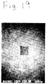
- Fig. 9 is a scanning electron microscope (SEM) photograph of an amorphous silicon film deposited at the temperature of 510°C with the deposition rate of 12.9 ⁇ /minute, showing a typical amorphous state.
- FIG. 9 This photograph in Fig. 9 is an as-deposited amorphous film (before thermal oxidation). If this film is thermally oxidized, it will change the crystalline structure from an amorphous state to polycrystalline one that is shown in Fig. 4. As can be seen from Fig. 9, no regions that can be termed islands can be discerned by SEM in this amorphous film before thermal oxidation. Therefore, it has been believed that regions called islands do not exist in an amorphous film.
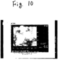
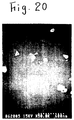
- Fig. 10 shows an atomic force microscope (AFM) photograph of an as-deposited amorphous silicon film, that is, a silicon film in an amorphous state immediately after the deposition, deposited at a deposition temperature of 510°C and a deposition rate of 12.9 ⁇ /minute.
- AFM atomic force microscope
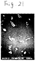
- FIG. 12 is a scanning electron microscope (SEM) photograph showing the silicon film in a polycrystalline state after thermal oxidation of this film.
- SEM scanning electron microscope
- the size of the islands (regions), which make up the as-deposited film clearly has a strong correlation with the size of the grains, which make up the polycrystalline film obtained by thermal oxidation of the as-deposited film.
- the as-deposited film being made up of large islands (regions) is thermally oxidized, thermal oxide film and a polycrystalline film which is made up of large grains are obtained.
- all the silicon films of the thin-film semiconductor device in accordance with the present invention are in an amorphous state immediately after they are deposited by LPCVD. Further, the size (diameter) of the islands (regions) that make up these amorphous films is within a distribution range of 100 nm to approximately 400 nm, for the case shown in Fig. 10, for example.
- the average island area of the as-deposited amorphous film is roughly the same as the average grain area of the polycrystalline film after thermal oxidation, or maybe slightly smaller, and it is more than 10,000 nm 2 when the deposition temperature and deposition rate are optimized.
- the silicon films of the comparative examples that are used in thin-film semiconductor device in prior art are normally deposited at a temperature of higher than 580°C. These films are in a polycrystalline state immediately after they are deposited by LPCVD, and the size (diameter) of the regions that make up these polycrystalline films is within a distribution range of 20 nm to approximately 80 nm. The average area of the regions in this case is no more than 10,000 nm 2 .
- Fig. 13 is a scanning electron microscope (SEM) photograph showing a silicon film in a polycrystalline state before thermal oxidation (an as-deposited polycrystalline silicon film), when the deposition temperature is 600°C.
- the size of the regions making up the amorphous film is, as expected, between 20 nm and approximately 80 nm.
- the sizes of the regions making up the as-deposited semiconductor film are distributing in the range of more than 100 nm in diameter, then the average grain size of the polycrystalline semiconductor film obtained after thermal oxidation will be increased to 10,000 nm 2 or more in area, and thus a high-performance thin-film semiconductor device will be fabricated.
- this second embodiment has been described with reference to an intrinsic silicon film as an example, it is obvious to those skilled in the art and universally valid that a large-grained polycrystalline semiconductor film could be obtained by firstly controlling the semiconductor film deposition process to deposit a thin film having large regions and by secondly subjecting the film to thermal oxidation, thus creating a high-performance thin-film semiconductor device.
- the present invention is effective not only with an intrinsic silicon film, but also with an impurity-doped silicon film or with other semiconductor films, such as a silicon germanium film, regardless of their nature of containing donors or acceptors.
- the method of depositing the semiconductor film is not limited to LPCVD, the film can equally well be deposited by plasma-enhanced CVD or sputtering.
- the average area of the islands (regions) making up the semiconductor film immediately after the film formation by one of these methods is at least 10,000 nm 2 , a large-grained polycrystalline film can be obtained by thermal oxidation, thus fabricating a high-performance thin-film semiconductor device.
- the present invention deposits a semiconductor film under conditions such that the nucleus generation rate is retarded and the island growth rate is accelerated.
- the point is how to control both the nucleus generation rate and the island growth rate simultaneously.
- the nucleus generation rate is controlled by the deposition temperature (temperature of the substrate surface) and the island growth rate is controlled by the deposition rate, by way of example.
- the nucleus generation rate is retarded by lowering the deposition temperature and the island growth rate is accelerated by increasing the deposition rate.
- the methods used to control the nucleus generation rate and the island growth rate are not limited to the above methods; for example, the nucleus generation rate may be retarded by means such as a change in the material of the substrate.
- One possible way of changing the material of the substrate is to use a special silicon dioxide film.
- the deposition rate may be increased either by increasing the flow rate of the reactant gas, such as mono-silane or di-silane, or by increasing deposition pressure.
- the deposition rate is also related to the deposition temperature, such that the deposition rate increases as the deposition temperature rises.
- the deposition temperature is fixed low, thereby retarding the nucleus generation rate.
- the flow rate of the reactant gas is increased or the deposition pressure is raised. This enables the implementation of a control method that does not contradict the principle of the present invention.
- the deposition temperature of the semiconductor film used for TFTs in prior art is within a customary range of 600°C to 650°C. It is clear from Fig. 3 that it is impossible to obtain a good-quality semiconductor film with high carrier mobility under these conditions, namely the high deposition temperature, even if the flow rate of reactant gas and deposition pressure are controlled to accelerate the deposition rate, because the high temperature accelerates the nucleus generation rate faster than the flow rate or pressure increases the island growth rate, and thus the islands making up the as-deposited film would be too small.
- the deposition rate does not depend only on the deposition temperature, the flow rate of the reactant gas, and the deposition pressure; it is also related to factors such as the volume of the LPCVD apparatus and the total reactive area when substrates are inserted into the LPCVD chamber. For example, if the total reactive area is large, the deposition rate is retarded even with the same flow rate of reactant gas.
- the factors that determine the deposition rate are discussed in detail in, for example, J. App. Phys. 74 (4), August 15, 1993, pp. 2870-2885.
- the deposition rate is a function of the concentration of the reactant gas in vapour phase, with the deposition rate accelerating as this concentration increases.
- the concentration of the reactant gas is a function of the partial pressure and temperature of the reactant gas, with the concentration increasing as the partial pressure of the reactant gas increases, and the concentration decreasing as the temperature of the reactant gas increases.
- the temperature of the reactant gas is determined by the pumping speed of the pump exhausting from the chamber and the flow rate of the reactant gas.
- the deposition pressure is also related to the functions of the pump, or to factors such as the flow rate of the reactant gas. In any case, the deposition rate can be controlled by the flow rate of the reactant gas and the deposition pressure, if parameters such as the deposition temperature, volume of the LPCVD apparatus, and total reactive area are fixed.
- the nucleus generation rate is also weak function of the flow rate of the reactant gas and the deposition pressure. However, the stronger factor affecting the nucleus generation rate is the deposition temperature. Increasing the flow rate of the reactant gas and raising the deposition pressure have a stronger effect on accelerating the deposition rate than on accelerating the nucleus generation rate.
- the deposition rate generally corresponds to the value that the deposited film thickness divided by the deposition time, where the deposition time is equivalent to the sum of the time required for the nuclei to be generated and the time required for the islands to grow.
- the island growth rate is equivalent to the value that the deposited film thickness differentiated by the deposition time. Therefore, strictly speaking, the deposition rate is related to the island growth rate but in fact they are not equal.
- the time required for the nuclei to be generated is usually sufficiently smaller than the time taken to deposit a film of several hundreds of ⁇ that the deposition rate and the island growth rate are almost the same.
- the deposition rate DR coincides with the island growth rate within experimental errors.
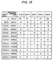
- Fig. 14 is a characteristic diagram showing the relationship between deposition temperature and average grain area after thermal oxidation. Note that in Fig. 14, the points indicated by squares are the average values calculated from the data listed in Figs. 15 and 6A. As shown in Fig. 14, a deposition temperature of 580°C acts as the first boundary below which the average grain area becomes extremely large. However, as also shown in this figure, the maximum value of the average grain area can be utilized by setting this temperature below the second boundary, ie. preferably 550°C or less. Similarly, Fig.
- FIG. 16 is a characteristic diagram showing the relationship between deposition temperature and leakage current when the transistor is in off state.
- the leakage current when the transistor is in off state is dramatically reduced at a deposition temperature of 530°C or less.
- the leakage current when the transistor is in off state will be large, if the active layer of the transistor consists of the crystals containing many defects.
- a lower limit to the deposition temperature is determined by factors such as the type of reactant gas, so that if the reactant gas is mono-silane, for example, the lower temperature limit is 460°C; if it is di-silane, the lower temperature limit is 370°C.
- Fig. 14 if the deposition temperature is less than 500°C, the grain area becomes less, but this is when the reactant gas is mono-silane. This does not occur with di-silane or other reactant gases. This is because, if the deposition temperature is less than 500°C with mono-silane, it will be hard to keep the deposition rate high. However, this is not the case for di-silane.
- the finished thermal oxide film inherits the surface configuration of the original pre-oxidation semiconductor film. Since a gate electrode is formed over such an oxide film in a MOS field-effect transistor (FET), the surface configuration of the as-deposited semiconductor film (immediately after its deposition by a method such as LPCVD) is reflected in the surface configuration of the boundary between the gate insulation film and the gate electrode. In other words, if the as-deposited semiconductor film is smooth, the boundary surface between the gate insulation film and the gate electrode will also be smooth; if the as-deposited semiconductor film surface has a certain amount of roughness, the boundary surface between the gate insulation film and the gate electrode will also have that roughness.
- FET MOS field-effect transistor
- the roughness of the boundary surface between the gate insulation film and the gate electrode has an effect on the breakdown voltage between source and gate or between drain and gate after the thin-film semiconductor device is fabricated. If the boundary surface is rough, electric field easily focuses on the peak of the gate electrode, making the electric field locally and extremely high on the peak, which can easily cause avalanche breakdown between the source and the gate or the drain and the gate.
- the as-deposited semiconductor film surfaces of the thin-film semiconductor devices in accordance with this embodiment are extremely smooth, so are the gate insulation film surface after thermal oxidation, such that they have center line average height (Ra) of 1.995 nm with the interval estimation value of 0.323 nm at the 95% confidential level.
- the as-deposited semiconductor film surfaces of the thin-film semiconductor devices in accordance with the comparative examples are rough, regardless of the deposition temperature, with the gate insulation film surfaces after thermal oxidation having center line average height (Ra) of 3.126 nm with the interval estimation value of 0.784 nm at the 95% confidential level.
- center line average height is the value that the total area of sections obtained by reflecting the roughness curve by the center line, divided by the measured length.
- the breakdown voltage between source and gate has been measured for all the six thin-film semiconductor devices in accordance with the present invention (the circles in Fig. 3).
- Each of the six devices supplies three samples for the measurement.
- eighteen devices have been measured in their breakdown voltage.
- the measurement has been done under the condition that the source of each sample is electrically grounded and the negative voltage is applied to the gate.
- all the eighteen samples have very good characteristics in the breakdown voltage, having the value of more than 100 V (equivalent to a breakdown electric field of more than 8.333 Mv/cm).
- eleven testpieces of each of three samples of the thin-film semiconductor devices of the comparative examples (the crosses in Fig.
- Thin-film semiconductor devices have been fabricated by the fabrication process described in the first embodiment, except that the reactant gases used in the LPCVD has been varied.
- semiconductor films have been deposited using di-silane (Si 2 H 6 ) of purity of at least 99.99% as reactant gas, using the LPCVD apparatus described previously with respect to the first embodiment.
- the deposition temperature is 450°C and di-silane is introduced at 100 sccm into the reaction furnace.
- Helium of purity of at least 99.9995% is used as the dilution gas introduced at 100 sccm into the reaction chamber.
- the pressure is 0.3 Torr and the deposition rate is 19.97 ⁇ /minute.
- the thus-obtained silicon films are in an amorphous state and have film thickness of 1000 ⁇ .
- the islands (regions) making up each amorphous film are of sizes with a distribution of 150 nm to approximately 450 nm.
- these amorphous films After being patterned, these amorphous films have been subjected to thermal oxidation at 1160°C in a 100% oxygen environment at one atmospheric pressure for 23 minutes, 36 seconds.
- the surface roughness of the gate insulation film after thermal oxidation is 1.84 nm in center line average height (Ra).
- the gate insulation film is removed by a 10% aqueous solution of hydrogen fluoride to have a SEM observation of the surface of the polycrystalline silicon film after the oxidation, it will show that the average area and standard deviation of area of the grains which consist of the polycrystalline silicon films are 14,110 nm 2 and 15,595 nm 2 respectively.
- the transistor characteristics of these thin-film semiconductor devices formed by the fabrication process described with reference to the first embodiment have been measured, with the results as given below.
- the measurement conditions and the definitions of ON and OFF currents and carrier mobility are the same as those of the first embodiment.
- the result is that the thin-film semiconductor devices show good characteristics, having high ON-current of 53.5 ⁇ A and low OFF-current of 0.154 pA with carrier mobility of 78.5 cm 2 /V.s, even when absolutely no hydrogenation has been performed.
- the breakdown voltage between source and gate has been measured for these three thin-film semiconductor devices, and is at least 100 V for all the devices.
- the ON-current will be improved to 77.7 ⁇ A
- the OFF-current be improved to 0.137 pA
- the carrier mobility be improved to 107 cm 2 /V.s.
- the average grain area of the resultant polycrystalline silicon film is at least 10,000 nm 2 , the boundary surface between the gate insulation film and the gate electrode is smooth, and thus a high-performance thin-film semiconductor device is provided, without being limited by the use of mono-silane as the type of reactant gas.
- the fundamental concept of the present invention is based on the principle that the nucleus generation rate can be retarded by lowering the deposition temperature and the island growth rate can also be accelerated, so that the regions (islands) making up the semiconductor film are large and have smooth surface. Therefore, the present invention is completely valid for any means of reducing the nucleus generation rate and increasing the island growth rate.
- Di-silane is used as the reactant gas in this third embodiment, but the present invention is effective with any reactant gas that provides a suppression of the nucleus generation rate by keeping the deposition temperature to 580°C or less and accelerates the island growth rate by a deposition rate of 6 ⁇ /minute or more, such as tri-silane (Si 3 H 6 ), a fluoro-silane (Si n H x F y : where n, x, and y are integers), or a chloro-silane (Si n H x Cl y : where n, x, and y are integers).
- any reactant gas that provides a suppression of the nucleus generation rate by keeping the deposition temperature to 580°C or less and accelerates the island growth rate by a deposition rate of 6 ⁇ /minute or more, such as tri-silane (Si 3 H 6 ), a fluoro-silane (Si n H x F y : where
- Thin-film semiconductor devices are fabricated by the fabrication process described in the section on the first embodiment, except that the thermal oxidation temperature used for forming the gate isolation layer is varied.
- intrinsic silicon films are deposited to film thickness of 1000 ⁇ by LPCVD on quartz substrates.
- the deposition conditions are the same as those of the first embodiment. That is, the deposition temperature is 510°C, mono-silane of purity of at least 99.99% is used as the reactant gas, and the gas is supplied to the reaction chamber at a flow rate of 100 sccm.
- the deposition pressure is 0.8 Torr and a silicon film is formed on each substrate under these conditions at a deposition rate of 21.5 ⁇ /minute.
- the thus-deposited silicon films are subjected to patterning, then a silicon dioxide film forming a gate insulation layer is formed by thermal oxidation on the silicon film surface.
- the thermal oxidation temperature is varied to be 1160°C, 1100°C, 1050°C, 1000°C, 950°C, and 900°C, respectively.
- the thermal oxidation furnace is initially held at 800°C with an 100% oxygen environment at one atmospheric pressure. After substrates are inserted in the thermal oxidation furnace in this state, the temperature is increased to the desired oxidation temperature at a heating rate of 10°C/minute. After the oxidation temperature has been reached, that state is maintained for the time appropriate to that particular temperature, as the thermal oxidation proceeds.
- the thickness of the thermal oxidation film obtained by this process is 1200 ⁇ at all of the thermal oxidation temperatures, and the thickness of the polycrystalline silicon film acting as the active layer of the thin-film semiconductor device is 400 ⁇ .
- the thin-film semiconductor devices are completed by exactly the same fabrication process as that of the first embodiment, except that final hydrogenation is not performed by this fourth embodiment.
- the transistor characteristics of the thus-obtained thin-film semiconductor devices are shown at A in Fig. 18, where ON current is plotted along the Y-axis, thermal oxidation temperature is plotted along the upper X-axis, and the inverse of the absolute thermal oxidation temperature is plotted along the lower X-axis.
- Fig. 18 shows that the transistor characteristic deteriorates as the thermal oxidation temperature Is reduced, but this deterioration is comparatively small in the thin-film semiconductor devices formed in accordance with the present invention.
- B in Fig. 18 shows the dependency on thermal oxidation temperature of the transistor characteristics of thin-film semiconductor devices formed as comparative examples.
- Each of the comparative-example thin-film semiconductor devices is formed by the above described fabrication method after the silicon film which is to act as the active layer is deposited with a deposition temperature of 600°C, a mono-silane flow rate of 100 sccm, a deposition pressure of 40 m Torr, and a deposition rate of 38.1 ⁇ /minute. It is clear from the figure that the characteristic of the thin-film semiconductor devices of the comparative examples deteriorates dramatically as the thermal oxidation temperature is reduced, so that in fact it becomes impossible to reduce the thermal oxidation temperature.
- the thin-film semiconductor devices of the present invention have superior characteristics, such that even devices obtained with a thermal oxidation temperature of 900°C have better characteristics than the thin-film semiconductor device obtained as comparative examples with a thermal oxidation temperature of 1160°C.
- the surface roughness of the MOS boundary surface (boundary surface between the semiconductor layer and gate insulation layer) deteriorates when the thermal oxidation temperature is approximately 1100°C or less, and the degree of this surface roughness becomes even worse as the thermal oxidation temperature is reduced.
- the MOS boundary surface is extremely stable so that the roughness of the MOS boundary surface does not become too bad even if the thermal oxidation temperature is reduced..
- Figs. 19, 20, and 21 are scanning electron microscope (SEM) photographs showing the state of a MOS boundary surface of the thin-film semiconductor device of this embodiment when the thermal oxidation temperature is 1160°C, 1050°C, and 900°C, respectively.
- Figs. 22, 23, and 24 are scanning electron microscope (SEM) photographs showing the state of a MOS boundary surface of the thin-film semiconductor device of the comparative example, when the thermal oxidation temperature is 1160°C, 1050°C, and 900°C, respectively.
- SEM scanning electron microscope
- Thin-film semiconductor devices are often formed on high-melting-point quartz glass.
- the thermal oxidation temperature is reduced, deformation such as expansion, contraction, or warping of the substrate can be reduced, enabling the fabrication of high-density, highly integrated devices.
- a lower temperature is also preferable from the viewpoints of apparatus lifetime and maintenance.
- This fifth embodiment shows how the present invention can be applied to low-temperature process.
- LCDs liquid crystal displays
- the active matrix method enables an LCD with several hundreds of thousands of pixels, with a switching transistor formed for each pixel.
- a transparent insulating substrate of a material such as fused quartz plate or glass is used as the substrate for various types of LCD, because it enables a transparent display.
- a semiconductor film of a material such as amorphous silicon or polycrystalline silicon is generally used as the active layer of each thin-film transistor (TFT), but polycrystalline silicon is preferable to amorphous one for integrating a driver circuit with the TFTs.
- the polycrystalline silicon operates faster in speed than does amorphous one.
- the active layer is made of a polycrystalline silicon film
- a fused quartz plate is used as the substrate and the TFT is fabricated by a method called high-temperature process where the maximum processing temperature usually exceeds 1000°C.
- the active layer is an amorphous silicon film
- an ordinary glass substrate is used.
- an amorphous silicon film has such inherent problems like its electrical characteristics are inferior to those of a polycrystalline silicon film and it has a slower operating speed.
- a-Si amorphous silicon
- LPCVD LPCVD at a deposition temperature of 550°C
- SiH 4 mono-silane
- the a-Si film is subjected to laser irradiation to convert the a-Si film into a poly-Si film.
- an SiO 2 film is deposited as a gate insulation film by electron cyclotron resonance chemical vapor deposition (ECR-PECVD) at a substrate temperature of 100°C.
- ECR-PECVD electron cyclotron resonance chemical vapor deposition
- a gate electrode is then formed of tantalum (Ta) on the gate insulation film, and the gate electrode is used as a mask for the ion implantation of a donor or acceptor impurity into the silicon film to form the source and drain of the transistor in a self-aligned manner.
- a non-mass-separated type of implantation apparatus is used for this ion implantation, with phosphine (PH 3 ) or diborane (B 2 H 6 ) diluted with hydrogen as the reactant gas.
- the implantation ions are activated at 300°C.
- An interlayer insulation film is then deposited and electrodes and wiring of indium tin oxide (ITO) or aluminum (Al) are formed to complete the thin-film semiconductor device.
- the fifth embodiment of the present invention described below is intended to solve these problems and to enable a practicable and simple method of fabricating a good thin-film semiconductor device.
- This fifth embodiment also fabricates a thin-film semiconductor device stably at a low enough processing temperature to use an ordinary large glass substrate.
- FIG. 25A to 25D A process of fabricating a thin-film semiconductor device that can form an MIS type of field-effect transistor is shown in Figs. 25A to 25D.
- a 235 mm ⁇ (235 mm ⁇ 235 mm) plate of non-alkaline glass (OA-2, produced by Nippon Electric Glass Co., Ltd.) is used as a substrate 101, but any type and size of the substrate will be used if the substrate can withstand the maximum processing temperature.
- a silicon dioxide film (SiO 2 film) 102 to act as an underlying protective film is first formed by a method such as ordinary atmospheric-pressure chemical vapor deposition (APCVD), PECVD, or sputtering on the substrate 101.
- the SiO 2 film can be deposited by APCVD with a substrate temperature of 250°C to approximately 450°C and using mono-silane (SiH 4 ) and oxygen as the reactant gas.
- PECVD or sputtering can also deposit the SiO 2 film at a substrate temperature of room temperature to 400°C.
- a 2000 ⁇ SiO 2 film is deposited by APCVD at a temperature of 300°C using SiH 4 and O 2 as the reactant gas.
- an intrinsic silicon film that is to act as an active layer of the thin-film semiconductor device is deposited to thickness of approximately 500 ⁇ .
- This intrinsic silicon film is deposited by an infralow-pressure CVD (ILPCVD) apparatus with a flow of 200 sccm of mono-silane (SiH 4 ) as reactant gas, at a deposition temperature of 495°C, for 31 minutes.
- the ILPCVD apparatus used for the fifth embodiment has a volume of 184.5 L. Seventeen substrates are inserted face-downward in a reaction chamber held at 300°C. After the substrates are inserted, a turbo-molecular pump is turned on. After it reaches to stable rotation state, a leakage test is performed for 2 minutes.
- the leakage rate which is mainly due to the desorption of gases, is 3.3 ⁇ 10 -5 Torr/minute.
- the temperature is then raised over one hour from the insertion temperature of 300°C to the deposition temperature of 495°C.
- the initial 10 minutes of the temperature rise absolutely no gas is introduced into the reaction chamber and the temperature is increased in a vacuum state.
- the background pressure achieved by the reaction chamber is 5.4 ⁇ 10 -7 Torr.
- a 300-sccm flow of nitrogen gas of purity of at least 99.9999% is introduced to lead the equilibrium pressure in the reaction chamber of 3.0 ⁇ 10 -3 Torr.
- the deposition temperature in accordance with this fifth embodiment is 495°C and the deposition rate is 16.6 ⁇ /minute, both the deposition temperature and the deposition rate are within the respective ranges, which is shown in Fig. 3, of 580°C or less and 6 ⁇ /minute or more. Therefore, as described with respect to the first to fourth embodiments, the fifth embodiment can form a semiconductor film with good characteristics.
- the thus-obtained silicon film is a high-purity a-Si film.
- This a-Si film is then subjected to irradiation with optical energy or electromagnetic-wave energy for a short time to crystallize the a-Si, and thus converted into polycrystalline silicon (poly-Si).
- a xenon chloride (XeCl) excimer laser (wavelength of 308 nm) performs the irradiation.
- the full width at half maximum value of the laser pulses is 45 ns. Since the irradiation time is so short, the substrate is not heated during the crystallization of the a-Si to poly-Si, and thus problems such as deformation of the substrate do not occur.
- the laser irradiation is performed with the substrate at room temperature (25°C), in an air.
- the area irradiated by a single laser irradiation is an 8 mm ⁇ square-shaped area, and each irradiation is shifted by 4 mm.
- the first laser irradiation energy density is 160 mJ/cm 2 .
- the entire surface is subjected to a second laser irradiation at an energy density of 275 mJ/cm 2 .
- the scanning method is the same as that of the first laser irradiation; an 8 mm ⁇ square-shaped irradiation region being shifted by 4 mm in the Y direction and then the X direction.
- the entire substrate is crystallized uniformly from a-Si into poly-Si by this two-stage laser irradiation.
- an XeCl excimer laser is used as the means of irradiating optical energy or electromagnetic-wave energy, but any suitable energy source can be used provided the time taken to irradiate the energy is within a few tens of seconds.
- the irradiation can be from any of various types of laser, such as an ArF excimer laser, an XeF excimer laser, a KrF excimer laser, a YAG laser, a carbon dioxide gas laser, an Ar laser, or a dye laser, or from a lamp such as an arc lamp or tungsten lamp.
- irradiation is performed by an arc lamp
- improvement of the film quality from a-Si to poly-Si can be achieved by a lamp output of at least approximately 1 kW/cm 2 with an irradiation time of approximately 45 seconds. Since the energy irradiation time is so short, even during this crystallization, there is no deformation or cracking of the substrate due to heat.
- This silicon film is then patterned to form a channel-portion semiconductor film 103 that acts as the active layer of the transistor (Fig. 25A).
- an a-Si film to a poly-Si film by energy irradiation can be replaced by furnace annealing at a temperature of approximately 600°C or less.
- This method is called the solid-phase crystallization, and crystallization thereby is completed by between about 8 hours and 24 hours if the temperature is approximately 600°C.
- This can also be used to implement a method of fabricating a thin-film semiconductor device in which a low-temperature process and the solid-phase crystallization are combined.
- a gate insulation film 104 is then formed by ECR-PECVD or PECVD.
- a SiO 2 film is used as the gate insulation film of this fifth embodiment, deposited to thickness of 1200 ⁇ by PECVD (Fig. 25B).
- Mono-silane (SiH 4 ) and "laughing gas" (N 2 O) are used as the reactant gas for the PECVD and the substrate temperature is 300°C.
- Conditions are established such that a plasma is formed by rf waves at 13.56 MHz, the output is 900 W, and the degree of vacuum is 1.50 Torr.
- the flow rate of SiH 4 is 250 sccm and that of N 2 O is 7000 sccm.
- the deposition rate of the SiO 2 film is 48.3 ⁇ /s.
- the silicon film and as-deposited oxide film are exposed to an oxygen plasma to improve the MOS boundary surface and the oxide film.
- Mono-silane and laughing gas are used as the reactant gas in this fifth embodiment, but the present invention is not limited thereto.
- An organic silane such as TEOS (Si-(O-CH 2 -CH 3 ) 4 ) or an oxidizing gas such as oxygen could be used instead.
- an extremely ordinary PECVD apparatus is utilized, but the insulation film can equally well be formed by an ECR-PECVD apparatus. Regardless of the type of CVD apparatus and reactant gas used, the temperature at which the insulation film is formed is preferably 350°C or less.
- This condition is important for preventing thermal deterioration of the MOS boundary surface and gate insulation film, and it also applies for all the subsequent steps described below.
- the temperature of all processing steps after the formation of the gate insulation film must be held to 350°C or less. This ensures that a high-performance thin-film semiconductor device can be fabricated easily and stably.
- a thin film that is to become a gate electrode 105 is next deposited by a method such as sputtering, vapor deposition, or CVD.
- tantalum (Ta) is selected as the gate electrode material, and it is deposited by sputtering to thickness of 5000 ⁇ .
- the substrate temperature during the sputtering is 180°C, and argon (Ar) containing 6.7% of nitrogen (N2) is used as the sputtering gas.
- the content of nitrogen in the argon is optimally between 5.0% and 8.5%.
- the crystal structure of the tantalum film obtained under these conditions is mainly the ⁇ -structure, with a resistivity of 40 ⁇ cm. Therefore, the sheet resistance of the gate electrode in accordance with the fifth embodiment is 0.8 ⁇ / ⁇ .
- Post-deposition patterning is performed on the thin film that is to be the gate electrode, then ion implantation 106 of an element such as phosphorus is performed into the intrinsic silicon film, using a bucket type of mass non-mass-separated ion implantation apparatus (ion doping), to form source and drain portions 107 and a channel region 108 (Fig. 25C).
- ion doping mass non-mass-separated ion implantation apparatus
- 5% diborane (B 2 H 6 ) diluted with hydrogen is used as the reactant gas, with the implantation being at dose concentration of approximately 5 ⁇ 10 15 cm -2 with a high-frequency output power of 20 W to 150 W and an acceleration voltage of 60 kV.
- a suitable masking material such as a polyimide resin is used alternately to cover one of the p-channel or n-channel TFTs at a time, while the appropriate ion implantation is performed by the corresponding method described above.
- SiO 2 is formed by PECVD as the interlayer insulation film.
- the reactant gas used in the PECVD is TEOS (Si-(O-CH 2 -CH 3 ) 4 ) and oxygen (O 2 ), and the film is formed at a substrate temperature of 300°C.
- the plasma is formed by 13.56 MHz rf waves under conditions of an output power of 800 W and a degree of vacuum of 8.0 Torr.
- the flow rate of the TEOS is 200 sccm and that of the O 2 is 8000 sccm.
- the formation rate of the SiO 2 film is 120 A/s.
- the substrate is subjected to furnace annealing for one hour at 300°C in an oxygen environment to activate the implanted ions and anneal the interlayer insulation film.
- the temperature of this furnace annealing is preferably 300°C to 350°C.
- Contact holes are then opened and source/drain extraction electrodes 110 are formed by a method such as sputtering to complete the thin-film semiconductor device (Fig. 25 D).
- ITO Indium tin oxide
- Al aluminum
- the substrate temperature while these conductors are formed by sputtering is 100°C to approximately 250°C.
- the transistor characteristics of the thus-obtained thin-film semiconductor device are measured.
- the source-drain current lds is defined to be an ON current ION, and ION is found to be (20.6 + 1.67, - 1.48) ⁇ 10 -6 A with 95% confidential level.
- the OFF current IOFF is found to be (2.27 + 0.40, - 0.31) ⁇ 10 -12 A.
- the present invention easily implements an enormous good and uniform thin-film semiconductor device that have high carrier mobility, that vary the lds for nearly ten to the seventh order in response to a 10-V change in the gate voltage, and that also have very little variation, by a low-temperature process wherein the maximum processing temperature is set to 600°C or less.
- the present invention enables the use of inexpensive glass substrates because the maximum processing temperature is at the first process in the device fabrication, so that alignment error caused by the thermal processes is minimum. Since the initial a-Si film of this embodiment is made up of large regions, the size of the crystal grains after the crystallization is also large, thus providing high-performance electrical characteristics. In other words, an ideal a-Si film is obtained by optimizing the deposition conditions under which the initial a-Si film is formed, and a uniform high-quality poly-Si film is obtained by crystallizing this a-Si film.
- LPCVD at a deposition temperature of approximately 550°C or more is used without consideration of the deposition rate, or the substrate temperature set to approximately 400°C for PECVD without any considering the quality of the initial a-Si film. Therefore, various problems occurred such as non-uniformity and an inability to provide stable production.
- One more aspect of the present invention is the way in which the processing temperature after the poly-Si film is formed is held to 350°C or less. Under this condition, the quality of the MOS boundary surface and the insulation film can be highly stabilized.
- the present invention is particularly effective for the top gate type of TFT, as shown in Figs. 25A to 25D.
- a high-quality semiconductor film consisting of a polycrystalline silicon film can easily be formed at a low temperature of less than approximately 600°C. This makes it possible to dramatically improve the characteristic of the thin-film semiconductor device, as well as enable stable mass production. More specifically, the present invention has the effects described below.
- the processing temperature is low at less than 600°C, inexpensive glass can be used and thus the product price can be reduced. Since it is also possible to prevent warping of the glass under its own weight, the resultant liquid crystal display device can easily be made large.
- the fifth embodiment fabricates a good thin-film semiconductor device, that has a higher ON-current and lower OFF-current than does the prior art. In addition, variations in these currents are reduced in the fifth embodiment.
- the sixth to twelfth embodiments described below illustrate how optimization of factors such as processing conditions can provide LDD-type thin-film semiconductor devices (LDD-type TFT circuits) having high speeds and good characteristics.
- a TFT circuit of the sixth embodiment is a CMOS circuit using both p-channel and n-channel LDD-type TFTs. Since an LDD-type TFT has a high-resistance portion between a channel portion and source and drain portions thereof, the electric field is not concentrated at the drain edge of the channel, so that it has particular effects in reducing the OFF current and increasing the breakdown voltage between source and drain and that between gate and source. However, it does have a problem in that the high-resistance portions reduce the actual voltage applied to the channel portion and thus the ON current is reduced.
- LDD-type TFTs have not yet been used in CMOS circuits that are required to work in high-speed, though they are used in applications such as the switching elements of an active matrix portion or SRAM resistance elements.
- CMOS circuit of LDD-type TFTs is capable of high-speed operation.
- the high-speed LDD-type TFT of the present invention is not limited to a CMOS configuration; it can also be applied widely to NMOS and PMOS configurations.
- a gate insulation film 5 is formed on a thin semiconductor film 2 that is patterned in an island shape on an insulating substrate 1, and a gate electrode 6 is formed thereon.
- an impurity that is to form donors is implanted at low concentration into the thin semiconductor film at source and drain portions of an n-channel TFT, to form a thin n - semiconductor film 9.
- the impurity implantation dose in this case is approximately 1 ⁇ 10 13 cm -2 to 1 ⁇ 10 14 cm -2 , and preferably approximately 2 ⁇ 10 13 cm -2 to 5 ⁇ 10 13 cm -2 .
- the maximum impurity concentration of the thin n - semiconductor film 9 is that value multiplied by 10 5 (see the calculations below) and thus is approximately 1 ⁇ 10 18 cm -3 to 1 ⁇ 10 19 cm -3 , and preferably approximately 2 ⁇ 10 18 cm - 3 to 5 ⁇ 10 18 cm -3 .
- the impurity is then further implanted at high concentration into source and drain portions to form a thin n + semiconductor film 3.
- the impurity implantation dose in this case is approximately 5 ⁇ 10 14 cm -2 to 1 ⁇ 10 16 cm -2 , preferably approximately 1 ⁇ 10 15 cm -2 to 3 ⁇ 10 15 cm -2 . If the dose is within this range, the maximum impurity concentration of the thin n + semiconductor film 3 is that value multiplied by 10 5 and thus is approximately 5 ⁇ 10 19 cm -3 to 1 ⁇ 10 21 cm -3 , preferably approximately 1 ⁇ 10 20 cm -3 to 3 ⁇ 10 20 cm -3 .
- This process divides the island-shaped thin semiconductor film into three sections with differing resistances: an intrinsic semiconductor region of channel, high-resistance impurity-doped semiconductor regions on either side of an intrinsic semiconductor region of a channel portion, and a low-resistance impurity-doped semiconductor region of the source and drain portions.
- an impurity that is to form acceptors is implanted at low concentration into the thin semiconductor film at source and drain portions of a p-channel TFT, to form a thin p - semiconductor film 10, then at high concentration into source and drain portions to form a thin p + semiconductor film 4.
- the gate electrode is used as a mask for the implantation of impurities, so that boundaries between the thin n - semiconductor film 9 and the channel portion and between the thin p - semiconductor film 10 and the channel portion are self-aligned to the gate edge (self-aligned structure).
- Highly doped source and drain portions need not be formed by the impurity implantation into the intrinsic semiconductor film as described above; they could equally well be formed as island shapes of a thin n + semiconductor film or a thin p + semiconductor film that already contains an impurity. Since the current that flows when a reverse bias is applied must be as low as possible in a TFT, it is preferable that the (intrinsic) thin semiconductor film is as thin as possible. However, if this film is too thin, the aluminum wiring could protrude out of the substrate through the contact holes. Therefore, if the highly doped source and drain portions are formed as individual island-shaped thin semiconductor films, then the above mentioned phenomenon will be prevented and a further thin (intrinsic) semiconductor film will be possibly used as a channel.
- a interlayer insulation film 7 is formed over each of these TFTs, and a thin metal film 8 is patterned to form wiring and complete the CMOS TFT circuit.
- a thin polycrystalline silicon film, a thin amorphous silicon film, a thin semiconductor film of Te or the like, or a thin semiconductor film of a compound such as CdSe, can be used as the material of the thin semiconductor film 2.
- the reason why the LDD-type CMOS TFT circuit of Fig. 26 is more suited to high-speed operation than a CMOS TFT circuit of an ordinary structure, shown in Fig. 27, will now be discussed.
- the lengths of an overlapping portion Yjn of the n-channel TFT and an overlapping portion Yjp of the p-channel TFT, shown in Fig. 26, are smaller than the equivalent lengths in the TFTs of the ordinary structure shown in Fig. 27.
- the concentration of the impurity implanted into the thin n- semiconductor film 9 and the thin p- semiconductor film 10 is extremely small, so that the diffusion length along the direction of the channel is shortened.
- the capacitances of these overlapping portions work loads for the CMOS circuit as parasitic capacitances. Therefore, the LDD-type CMOS TFT circuit, which has smaller overlapping capacitance, will be operating at higher speed than be a TFT of an ordinary structure, if it has nearly the same ON-current as does the TFT of an ordinary structure.
- the effective n-channel channel length Leffn and the effective p-channel channel length Leffp are the lengths obtained by subtracting twice the corresponding overlapping portion Yjn or Yjp from the n-channel gate electrode length (see Fig. 26; note that the gate electrode length is sometimes called the gate electrode width) Lgaten and the p-channel gate electrode length Lgatep. Therefore, if the overlapping portions could be made small, the effective channel length would be increased and the ON current decreased. Since the overlapping portions of the LDD-type CMOS TFT are small, as described above, the effective channel length becomes somewhat longer than that of a TFT of an ordinary structure, if the gate lengths are the same between two type of TFTs, and the ON current is reduced.
- LDD structure when an LDD structure is implemented, the breakdown voltage between source and drain is markedly improved in practice, and thus the circuit can be configured with LDD TFTs having an extremely small gate electrode length. As a result, LDD structure can compensate for the reduced ON current by shortening both the gate electrode length and the effective channel length.
- the channel resistance Rch(on) when the TFT is in an ON state varies faster than linearly with the effective channel length Leff.
- the ON current of each TFT increases suddenly as the effective channel length shortens. Since the channel portion of a TFT is in a polycrystalline state, the number of grain boundaries within the channel decreases as the channel becomes shorter, and thus it is considered that their adverse effect on electrical conductivity is reduced.
- the current can be controlled somewhat by the parasitic resistance of the LDD portion, the current flowing through the components can be made greater in an LDD-type TFT with a short channel than in a TFT of an ordinary structure.
- FIG. 28 A characteristic diagram illustrating the relationship between gate electrode length and source-drain breakdown voltage in the LDD-type TFT of this embodiment and a TFT of an ordinary structure is shown in Fig. 28.
- the breakdown voltage between source and drain in the TFT of an ordinary structure deteriorates when the gate electrode length is 5 ⁇ m or less.
- the gate electrode lengths of both the p-channel TFT and the n-channel TFT of the ordinary structure must be made at least 5 ⁇ m, in order to reliably prevent the breakdown in voltage between source and drain.
- Fig. 28 A characteristic diagram illustrating the relationship between gate electrode length and source-drain breakdown voltage in the LDD-type TFT of this embodiment and a TFT of an ordinary structure.
- a reliable prevention of the source-drain breakdown (breakdown voltage of at least 20 V) can be obtained with the LDD-type TFT of this embodiment, even if the gate electrode length is 5 ⁇ m or less. Even if the gate electrode length is 3 ⁇ m, a breakdown voltage between source and drain of at least 20 V can be obtained. A breakdown voltage between source and drain of at least 15 V can still be obtained when the gate electrode length is 2 ⁇ m.
- the OFF current is also reduced by at least one order of magnitude compared with a TFT of an ordinary structure.
- FIG. 29 A characteristic diagram illustrating the relationship between gate electrode length and ON current in the LDD-type TFT of this embodiment and a TFT of an ordinary structure is shown in Fig. 29.
- the ON current of the TFT of an ordinary structure when the gate electrode length is 5 ⁇ m is about the same as the ON current of the LDD-type TFT when the gate electrode length is 4 ⁇ m.
- the ON current is reduced by the implementation of an LDD structure, an ON current of at least the same level as that of the ordinary structure can be obtained, provided the gate electrode length can be made small.
- LDD-type TFT causes no problems concerning low breakdown voltage, even when the electrode length is 4 ⁇ m, as can be seen from Fig. 28.
- the ON current of a TFT of the ordinary structure when the electrode length is 4 ⁇ m is about the same as the ON current of the LDD-type TFT when the electrode length is 3 ⁇ m. Even when the gate electrode length is 3 ⁇ m, there are no problems concerning low breakdown voltage, as is clear from Fig. 28. Since the source-drain breakdown voltage is very low when the gate electrode length is less than 4 ⁇ m in the TFT of the ordinary structure, it becomes impossible to measure the ON current. In contrast, the source-drain breakdown voltage of the LDD-type TFT with the gate length even of 2 ⁇ m of this embodiment is still high, so that the extremely high ON current is available as shown in Fig. 29.
- the LDD-type TFT of this embodiment can achieve a large size of ON current that can never be obtained by the TFT of the ordinary structure.
- the gate electrode length is, for example, less than 3 ⁇ m.
- applying an LLD structure both to a p-channel and n-channel TFT makes it possible to reduce the gate electrode length of either type of TFT to 5 ⁇ m or less, preferably 4 ⁇ m or less, and more preferably 3 ⁇ m or less, and thus enabling the CMOS circuit that works very fast in operation speed.
- the gate insulation film in the LDD-type TFT can be made thinner to, for example, 1000 ⁇ or less. Although making the gate insulation film thinner increases the channel capacitance, it increases the operating speed of the TFT circuit, because it simultaneously decreases the threshold voltage, and thus increases the ON current.
- CMOS inverter circuits are connected as shown in Fig. 30A, with the output of one gate connected to the input of the next-stage gate. If this simple two-stage inverter is considered, a first-stage transistor TFTp1 or TFTn1 charges or discharges the two channel capacitances of next-stage transistors TFTp2 and TFTn2, and the time constant set by this charge/discharge determines the switching speed.
- the channel length of the LDD-type CMOS TFT can be shortened as shown in Fig. 30C, an ON resistance Rp1 of the p-channel TFT and an ON resistance Rn1 of the n-channel TFT are reduced, and the magnitudes of a charge current ip1 and a discharge current in1 are increased. Since an overlapping capacitance Cp02 of the next-stage p-channel TFT and an overlapping capacitance Cn02 of the next-stage n-channel TFT are reduced as described above, and also a capacitance C2 of the channel portion is reduced by the shortening of the channel, the load capacitance under all of the bias conditions (ON state, OFF state, and an intermediate bias) is reduced.
- a short-channel LDD-type CMOS TFT circuit has a shorter charge/discharge time constant and a higher operating speed than a circuit with TFTs of the ordinary structure.
- the ON resistance Rp1 of the p-channel TFT and the ON resistance Rn1 of the n-channel TFT become somewhat higher, due to a higher resistance in the LDD portion, than those of the TFTs of the ordinary structure, the operating speed can be increased if the value of the time constant Rp1 ⁇ (Cp02 + Cn02 + C2) and of Rn1 ⁇ (Cp02 + Cn02 + C2) could be made smaller than those of the TFTs of the ordinary structure.
- Figs. 31A and 31B Examples of the actual transfer characteristics of TFTs formed with the configuration of Fig. 26 are shown in Figs. 31A and 31B. It can be seen from transfer characteristics 42 and 44 of LDD-type TFTs that the ON current is approximately 50% to 60% of that of transfer characteristics 41 and 43 of ordinary TFTs. Since TFTs of the same gate electrode length are compared, this is attributed to the longer effective channel length of LDD-type TFTs. Since the OFF current is greatly reduced, the ON/OFF ratio is increased by at least one order of magnitude. The breakdown voltage between source and drain and the breakdown voltage between source and gate are also greatly increased in the LDD-type TFT. Therefore, if the gate electrode length of an LDD-type TFT is halved, the ON current would remain at or above the same level and the OFF current would decrease by at least one order of magnitude, thus enabling an increase in the breakdown voltage.
- Fig. 32 Results of simulating the maximum operating frequency of a shift register circuit, based on the characteristics of the tested LDD-type TFT, are shown in Fig. 32.
- a short-channel LDD-type TFT circuit can operate at higher speed than a TFT circuit of the ordinary structure.
- the LDD-type TFT has a far smaller OFF current, the power consumption of a circuit driven at the same voltage can be reduced, even if the gate electrode length is reduced to about half.
- the breakdown voltage between source and drain and the breakdown voltage between source and gate are far larger with the LDD-type TFT, a high-voltage circuit can be configured if necessary.
- an electro-optical material that could not be driven by a TFT circuit of the prior art, because it requires a high drive voltage, can be driven easily by such a circuit with LDD-type TFTs.
- Examples of such an electro-optical material could be a high-molecular weight polymer dispersed liquid crystal (PDLC) or a guest/host type of liquid crystal.
- PDLC high-molecular weight polymer dispersed liquid crystal
- the threshold voltage of such a liquid crystal can be increased and, if this liquid crystal is used in a display element of a liquid crystal display device, the angle of visibility thereof can be greatly increased.
- the gate electrode length of the n-channel TFT is made to be longer than that of the p-channel TFT.
- the ON currents of the two TFTs are approximately the same.
- the resistance of the p-channel TFT must be made sufficiently small. From the point of view of spatial efficiency in the layout, it is more effective to vary the channel length with a constant channel width, than vary the channel width with a constant channel length.
- the channel length could be fixed as the minimum dimension of the gate electrode length, and the n-channel width could be made smaller than the p-channel width.
- the channel lengths or widths of the p-channel and n-channel TFTs can be determined comparatively easily.
- a circuit in which the connections of TFTs of the same polarity are mixed in parallel and in series, such as a NAND gate or NOR gate it will be necessary to optimize the size of each TFT to suit the objective of that circuit.
- FIG. 33A, 33B, and 33C A circuit diagram, a pattern diagram, and a wafer cross-sectional view when a CMOS inverter circuit is configured of a single-crystal MOSFET are shown in Figs. 33A, 33B, and 33C, respectively.
- Fig. 34 a pattern diagram when a CMOS inverter circuit is configured of a TFT is shown in Fig. 34.
- a single-crystal MOSFET With a single-crystal MOSFET, a p-well is necessary for forming the n-channel transistor, and thus the p-channel transistor and the n-channel transistor cannot be place too close together.
- a single-crystal MOSFET must also be provided with a p + stopper (guard bar) in a p- well or an n + stopper in an n- bulk in order to stabilize the potential of the well or n-bulk and prevent the occurrence of latch-up.
- This stopper must be provided at the boundary between the p-channel transistor and the n-channel transistor, and thus the p-channel transistor and the n-channel transistor must be located even further apart. For that reason, the length in the lateral direction of Fig. 33 is large and thus the area occupied by this circuitry is also large. In contrast, the island-shaped thin semiconductor films of a TFT are completely insulating. Therefore, as shown in Fig. 34 (corresponding to the cross-sectional view of Fig.
- the fabrication methods of the first to fifth embodiments plus further use of the LDD structure make it possible to increase the speed of the TFT. If the operating speed could be made to be close to that of a single-crystal MOSFET, the above advantage concerning layout could be used to substitute the TFT configuration into circuits that have had to use single-crystal MOSFETs up until now.
- TFTs also have the advantage that there are many ways in which their patterns can be arranged, as shown in Fig. 34, and their layout efficiency can also be increased by the channel width constant while varying the channel length.
- This embodiment relates to optimization of the conditions for fabricating an LDD-type TFT.
- This embodiment first optimizes the maximum impurity concentration (dose) of the LDD portion, then optimizes the maximum impurity concentration (dose) of the source and drain portions, and finally optimizes the LDD length.
- this embodiment is designed to increase the speed and increase the breakdown voltage of an LDD-type TFT.
- a characteristic diagram showing the relationship between dose of the LDD portion and ON and OFF currents is shown in Fig. 35
- a characteristic diagram showing the relationship between dose of the LDD portion and ON/OFF ratio (ON current/OFF current) is shown in Fig. 36
- a characteristic diagram showing the relationship between dose of the LDD portion and sheet resistance of the LDD portion is shown in Fig. 37.
- polycrystalline semiconductor films are prepared in accordance with the first fabrication method described in the section on the background of the invention, with film thickness of approximately 500 ⁇ . It is clear from Fig. 35 that if the dose of the impurity implanted into the LDD portion is too high, it is impossible to reduce the OFF current.
- Fig. 35 shows that the OFF current drops dramatically at doses of 1 ⁇ 10 14 cm -2 or less.
- the dose of the LDD portion is high, the concentration of electric field at the drain edges cannot be restrained, and thus the OFF current increases, lowering the breakdown voltages between source and drain and between source and gate. Therefore the dose of the LDD portion is preferably 1 ⁇ 10 14 cm -2 or less, and thus the maximum impurity concentration of the LDD portion is preferably that value multiplied by 10 5 , which is 1 ⁇ 10 19 cm -3 or less.
- the dose of the LDD portion is preferably 1 ⁇ 10 13 cm -2 or more.
- the ON/OFF ratio is at a maximum when the dose is between 1 ⁇ 10 13 cm -2 and 1 ⁇ 10 14 cm -2 , as shown in Fig. 36, optimally between approximately 2 ⁇ 10 13 cm -2 and 5 ⁇ 10 13 cm -2 .
- the dose of the LDD portion is preferably in the range of approximately between 1 ⁇ 10 13 cm -2 and 1 ⁇ 10 14 cm -2 and the maximum impurity concentration is preferably in the range of approximately between 1 ⁇ 10 18 cm -3 and 1 ⁇ 10 19 cm -3 . More preferably, the dose of the LDD portion is in the range of approximately between 2 ⁇ 10 13 cm -2 and 5 ⁇ 10 13 cm -2 and the maximum impurity concentration is in the range of approximately 2 ⁇ 10 18 cm -3 to 5 ⁇ 10 18 cm -3 . This optimizes the maximum impurity concentration of the LDD portion.
- the dose of the LDD portion should be 1 ⁇ 10 14 cm -2 or less.
- no lower limit is disclosed with this prior art technique, and there is absolutely no suggestion that there could be a maximum value of the ON/OFF ratio in the dose range of 1 ⁇ 10 14 cm -2 to 1 ⁇ 10 13 cm -2 .
- the very idea of optimizing the maximum impurity concentration of the LDD portion in this seventh embodiment cannot exist in the techniques of single-crystal LDD-type MOSFETs.
- the LDD length of a single-crystal LDD-type MOSFET is as short as, for example, approximately 0.1 ⁇ m and thus the resistance of this LDD portion has virtually no effect on operating speed. Therefore, there is no need to consider the maximum impurity concentration of the LDD portion with an LDD-type MOSFET.
- impurity ions acceleratingly diffuse along with the grain boundaries (accelerated diffusion) in a non-single-crystal LDD-type TFT as described previously, the LDD length must be made longer than that of a single-crystal MOSFET.
- the sheet resistance of the LDD portion is not negligible and, in order to implement higher speeds, it is necessary to consider the idea of optimizing the maximum impurity concentration at the LDD portion.
- FIG. 38 shows that diffusion length increases as the dose of impurities implanted in the source and drain portions increases. If the diffusion length becomes too large, impurities diffuse into the LDD portion from the drain or source portion, causing problems such as a reduction of the effective LDD length of the LDD portion to zero.
- the LDD length is determined by the dimensions of the photoresist mask.
- the aim is to shorten the channel by making the gate electrode length 5 ⁇ m or less, so in order to miniaturize the components the LDD length cannot be set too long, and thus it is preferable that the LDD length is, for example, 4 ⁇ m or less.
- the dose of the source and drain portions becomes larger than 1 ⁇ 10 16 cm -2 , the diffusion length also increases to more than 4 ⁇ m, as shown in Fig. 38.
- the dose of the source and drain portions is 1 ⁇ 10 16 cm -2 or less.
- the contact resistance at the source and drain portions increases.
- this contact resistance is set as low as possible, to, for example, 3 k ⁇ or less for a contact hole sized 10 ⁇ m ⁇ (3k ⁇ /100 ⁇ m 2 ). It is also preferable in this case that the dose of the source and drain portions is at least 5 ⁇ 10 14 cm -2 , as shown in Fig. 39. This reduces the contact resistance and enables an increase in speed of the LDD-type TFT.
- the LDD length is preferably in the range of approximately between 1 ⁇ m and 2 ⁇ m. Therefore, the dose of the source and drain portions in this case is in the range of approximately between 1 ⁇ 10 15 cm -2 and 3 ⁇ 10 15 cm -2 , as is clear from Fig. 38.
- the dose in the source and drain portions is in the range of approximately between 5 ⁇ 10 14 cm -2 and 1 ⁇ 10 16 cm -2 and the maximum impurity concentration is in the range of approximately between 5 ⁇ 10 19 cm -3 and 1 ⁇ 10 21 cm -3 . More preferably, the dose in the source and drain portions is in the range of approximately between 1 ⁇ 10 15 cm -2 and 3 ⁇ 10 15 cm -2 and the maximum impurity concentration is in the range of approximately between 1 ⁇ 10 20 cm -3 and 3 ⁇ 10 20 cm -3 . This optimizes the maximum impurity concentration of the source and drain portions.
- the dose of the source and drain portions should be in the range of between 1 ⁇ 10 14 cm -2 and 1 ⁇ 10 17 cm -2 .
- this lower numerical value, 1 ⁇ 10 14 cm -2 is nothing more that a limit that ensures that the dose is greater than that of the LDD portion.
- a practical problem with setting the dose to 1 ⁇ 10 14 cm -2 concerns the way in which the contact resistance becomes approximately 50 k ⁇ for a contact hole having the area of 100 ⁇ m 2 , as shown in Fig. 39, which cannot be borne by the LDD-type TFT of this embodiment.
- the gate channel length with this prior art technique is 6 ⁇ m and thus the ON resistance is so much higher than that of this embodiment, there is no need to worry about lowering such a contact resistance in the prior art.
- the upper limit of the dose with this prior art technique is 1 ⁇ 10 17 cm - 2 , but a dose so large increases the diffusion length excessively, as shown in Fig. 38.
- the gate channel length is 6 ⁇ m, the LDD length need not be shortened by that amount, and thus the upper limit can be made so large.
- this prior art technique discloses absolutely nothing about the idea of optimizing the maximum impurity concentration of the source and drain portions to enable the LDD-type to operate at high speed and with a high breakdown voltage.
- the very idea of optimizing the maximum impurity concentration of these source and drain portions in the seventh embodiment cannot exist in the techniques of single-crystal LDD-type MOSFETs. This is because the phenomenon of accelerated diffusion along the grain boundaries does not occur in a single-crystal LDD-type MOSFET, and thus there is no particular need to consider the effects of diffusion of the impurities from the source and drain portions. Proof of this lies in the way that the LDD length of a single-crystal LDD-type MOSFET is extremely short at, for example, approximately 0.1 ⁇ m.
- FIG. 40 A characteristic diagram showing the relationship between LDD length and ON and OFF currents is shown in Fig. 40, and a characteristic diagram showing the relationship between LDD length and source-drain breakdown voltage is shown in Fig. 41.
- the channel and LDD portions are thin polysilicon films with film thickness of 450 ⁇ .
- the dose of the LDD portion is 3 ⁇ 10 13 cm -2 .
- Fig. 40 shows that the OFF current drops suddenly at a certain LDD length and it decreases only slightly at longer LDD lengths.
- the ON current decreases a little at a certain LDD length then decreases gradually at longer lengths, but it only decreases by about one half, in contrast to the drop of at least two orders of magnitude in the OFF current.
- Fig. 41 shows that there is a huge increase in the breakdown voltage between source and drain (and the breakdown voltage between source and gate too) at the point at which the OFF current suddenly decreases. From observation of these phenomena, it is clear that it is better to ensure that the LDD lengths of all the TFTs in a circuit are greater than length at which the OFF current drops suddenly. If the LDD length is determined in a self-aligned manner by means such as side walls made by the insulation film, the thickness of that insulation film could be made thicker than the necessary LDD length.
- the minimum value of variations in the LDD length can be at least 1 ⁇ m, even when a fabrication method is used in which the LDD length is varied by mask alignment. Assuming that the differences in ON current are comparatively small with TFTs with slightly large LDD lengths, as seen in Fig. 40, this should not cause much of a problem in a digital circuit. With an analog circuit, it will be necessary to set the LDD length in such a manner that the resistance required in the circuit is satisfied, even at the previously estimated maximum LDD length.
- the optimum value of the LDD length can be considered as described below.
- the LDD length should be set to be in a range within which the effective LDD length is not reduced to zero by diffusion from the source and drain portions, and it should be as short as possible from consideration of component miniaturization. Therefore, the LDD length corresponding to the optimal dose of the source and drain portions (which is 5 ⁇ 10 14 cm -2 to 1 ⁇ 10 16 cm - 2 , preferably 1 ⁇ 10 15 cm -2 to 3 ⁇ 10 15 cm - 2 ) is preferably in the range of approximately between 0.6 ⁇ m and 4 ⁇ m, and more preferably in the range of approximately between 1 ⁇ m and 2 ⁇ m.
- the diffusion coefficient in a TFT using a non-single-crystal thin semiconductor film is at least one order of magnitude larger than that of a single-crystal semiconductor, because accelerated diffusion occurs along the grain boundaries.
- a design method that employs a MOSFET using a single-crystal semiconductor can not be applied to an LDD-type CMOS TFT circuit using a non-single-crystal thin semiconductor film.
- an LDD length of at least 1 ⁇ m is obtained for each of p-channel and n-channel polysilicon CMOS TFTs.
- the LDD length has large variations of approximately 1 to 4 ⁇ m.
- the TFT must either ensure the necessary ON current or operate at the speed necessary for the TFT circuitry, even if the sheet resistance of the LDD portion is maximized and the LDD length is also maximized, and thus a special design method that allows for such cases is necessary.
- Dedicated LDD-type CMOS TFT circuit models have been developed, which take into account large variations in the assumed range of the resistance of the LDD portion, and which can calculate the resultant effective voltage applied to the channel portion to estimate the ON current, and thus simulations have been performed.
- this embodiment concentrates on the ON current in the optimization of the LDD length and the amount of impurity implanted in the LDD portion, while greatly shortening the channels of both the p-channel and n-channel TFTs in comparison with the prior art.
- This embodiment also enables impurity implantation at low energy but a high throughput, in order to implant impurities from through a thin gate insulation film.
- optimization of the fabrication process enables the implementation of an LDD-type CMOS TFT that is the first to be suitable for high-speed operation.
- This embodiment relates to a method of fabricating a CMOS circuit in which an LDD-type TFT is used.
- Process diagrams of a typical method of fabricating polysilicon TFTs is shown in Figs. 42A to 42D.
- First a thin polysilicon film 72 patterned as islands is subjected to thermal oxidation to form a thermal oxidation SiO 2 film 73 for each TFT, then a gate electrode 74 is formed thereon as shown in Fig. 42A.
- Photoresist 75 is then coated over a p-channel TFT area, and an impurity that is to form donors is implanted at low concentration, as shown in Fig. 42B. Phosphorus ions are used.
- Photoresist is once again coated over the entire surface of the p-channel TFT and an area somewhat larger than the gate electrode of the n-channel TFT, as shown in Fig. 42C, and the impurity that is to form donors is implanted at high concentration. This completes the source and drain and channel portions of the n-channel LDD-type TFT. In the same manner, an impurity that is to form acceptors, such as boron ions, is implanted at low concentration and high concentration into regions of the p-channel TFT. Finally, an interlayer insulation film 76 is deposited and metal wiring 77 is patterned, as shown in Fig. 42D.
- LDD lengths can be used, depending on the type of circuit. If an element is always subjected to a fixed bias, the LDD structure of the element can be set for only a single electrode. For example, the LDD structure could be used for the drain portion only.
- an LDD-type TFT uses side walls made by an insulation film as a mask.
- the gate electrode could be covered by an insulation film made by thermal oxidation or anodic oxidation, or by a new insulation film that could be formed by a deposition method such as chemical vapor deposition and that could cover the electrode surface layer portion with the thickness of at least the necessary LDD length.
- a deposition method such as chemical vapor deposition and that could cover the electrode surface layer portion with the thickness of at least the necessary LDD length.
- sections with differing resistances are formed by ion implantation into the same thin semiconductor film, but patterning of the first thin semiconductor films which already have differing resistances and then depositing the second thin semiconductor films overlapping the first could be used instead.
- the one with the thinner channel portion has the better characteristics, but a thicker film is better for reducing the contact resistance of source and drain portions, so a method that forms a thick impurity-doped semiconductor film in source and drain portions only could be used.
- the method of fabricating a TFT of this embodiment can be applied to all LDD-type CMOS TFTs using non-single-crystal thin semiconductor films.
- This ninth embodiment combines a fabrication method based on the principle that the nucleus generation rate is retarded and the island growth rate is accelerated with a method of fabricating an LDD-type TFT.
- a solid-phase crystallization method is used in this ninth embodiment to convert the as-deposited film of an amorphous state to a polycrystalline state. The fabrication method of the ninth embodiment is described below with reference to Figs. 1A, 1B, and Figs. 42A to 42D.
- an intrinsic silicon film is deposited by LPCVD on a substrate 201. Quartz glass is used as this substrate without an underlying protective film deposited thereon, in order to simplify the process.
- a silicon dioxide (SiO 2 ) film could be deposited by CVD as an underlying protective film, before the semiconductor film is formed, as shown in Fig. 25A.
- the size of grains making up the semiconductor film which is of polycrystalline silicon after the thermal oxidation, can be made constant between substrates.
- an amorphous silicon film is first deposited.
- the thickness of the film after deposition is 950 ⁇ .
- the deposition temperature is 495°C, mono-silane (SiH 4 ) of purity of at least 99.99% is used as the reactant gas, and this gas is supplied into the reaction chamber at a flow rate of 200 sccm.
- the deposition pressure in this case is 1.3 Torr and the deposition rate of the silicon film under these conditions is 16 ⁇ /minute.
- the thus deposited silicon film is subjected to patterning to obtain a silicon film 202 (Fig. 1A).
- the substrate is then subjected to furnace annealing for approximately 24 hours at 600°C in a nitrogen atmosphere to convert the amorphous silicon film into a polycrystalline silicon film (solid-phase crystallization method).
- the furnace annealing temperature in this case is not limited to 600°C; it is preferably in the range of between 500°C and 700°C, and more preferably in the range of between 550°C and 650°C.
- the patterned surface of the silicon film 202 is subjected to a thermal oxidation method to form a silicon dioxide film 203.
- This thermal oxidation is performed at a temperature of 1000°C in a 100% oxygen environment at one atmospheric pressure.
- the thickness of the silicon film is thus reduced to 600 ⁇ , and thus a silicon dioxide film having film thickness of 700 ⁇ is obtained (Fig. 1B).
- a gate electrode 74 is then formed on the thermal oxidation SiO 2 film (Fig. 42A).
- the p-channel TFT is covered with photoresist 75 and an impurity that is to form donors is implanted at low concentration (Fig. 42B).
- Photoresist is once again coated over the entire surface of the p-channel TFT and an area somewhat larger than the gate electrode of the n-channel TFT, and the impurity that is to form donors is implanted at high concentration (Fig. 42C). This completes the source and drain and channel portions of the n-channel LDD-type TFT.
- an impurity that is to form acceptors such as boron ions, is implanted at low and high concentration into regions of the p-channel TFT.
- an interlayer insulation film 76 is deposited and metal wiring 77 is patterned, as shown in Fig. 42D.
- the LDD lengths of the thus-formed LDD-type TFTs are 2.0 ⁇ m on both the p-channel side and the n-channel side.
- the dose of the LDD regions is 2 ⁇ 10 13 cm -2 and the dose in the low-resistance source and drain portions (high-concentration regions) is 1 ⁇ 10 15 cm -2 .
- NMOS LDD n-channel LDD-type TFT
- PMOS LDD p-channel LDD-type TFT
- a sufficient ON current is obtained even when Vgs is 5 V or -5 V, thus enabling a lowering of the power voltage.
- the threshold voltage of both the NMOS LDD and the PMOS LDD has little dependency on Vds, enabling a shortening of the channel length.
- the dependency of the threshold voltage on Vds was extremely large, making these TFTs in the prior arts unsuitable for practicable use, while this embodiment of the present invention provides a much better characteristic.
- the contact resistance can also be made sufficiently small with this embodiment. Since the film quality of the polysilicon film of this embodiment is so good, the sheet resistance can be reduced even if the dose is lowered. In other words, the parasitic resistance of the source and drain portions can be reduced and the ON current can be increased.
- the contact resistance, source and drain resistance, and LDD resistance of the LDD-type TFTs in accordance with this embodiment and comparative examples are measured, with the results being as shown in Fig. 45.
- the comparative examples are prepared by the first fabrication method of the prior art.
- the contact resistance, source and drain resistance, and LDD resistance of the transistors of this embodiment are all less than those of the comparative examples.
- the source and drain resistances are far lower (one-fifth to one-fiftieth) than those of the comparative examples.
- the crystallinity of the polysilicon film of this embodiment is so high, the sheet resistance of the LDD portion is low, even when the dose of the LDD portion is low.
- the sheet resistance of the LDD portion is so high that it is not possible to avoid a drop in the ON current.
- sheet resistance of the LDD portion in accordance with this embodiment is low enough that the parasitic resistance generated within the LDD portion can be minimized.
- N(x) N0/(2 ⁇ ) 1/2 ( ⁇ Rp) ⁇ exp ⁇ -(X - Rp) 2 /2( ⁇ Rp) 2 ⁇
- the dose of the LDD portion of the NMOS TFT in the shift register of Fig. 44 is 2 ⁇ 10 13 cm -2 . Therefore, it can be seen from Fig. 45 that the sheet resistance of the LDD portion is 36 k ⁇ /n.
- the parasitic resistance in this case is calculated as follows:
- the parasitic resistance in accordance with this embodiment does not become large even if LDD is implemented. This tendency is particularly obvious with a PMOS LDD, as shown below.
- the contact portion is provided at high-concentration source and drain portions, and the doses are such that the dose in the high-concentration portions is 3 ⁇ 10 15 cm -2 and that in the LDD portion (low-concentration portion) is 2 ⁇ 10 13 cm -2 .
- the LDD length is 1 ⁇ m.
- the channel width is 10 ⁇ m and the channel length (gate length) is 2.5 ⁇ m.
- the dose of the high-concentration source and drain portions is 3 ⁇ 10 15 cm -2 , three times that of the examples in Fig. 45, their sheet resistance is 1/3 or less of 30 ⁇ / ⁇ .
- the length of the high-concentration source and drain portions is the distance to the center of the contact hole (4.5 ⁇ m) less the LDD length (1 ⁇ m).
- the minimum channel length must be more than 5 ⁇ m and it is not possible to have an implantation dose of 1 ⁇ 10 15 cm -2 or less.
- the contact resistance taken from Fig. 45 is given by:
- the channel resistance in the ON state is increased more than twice in comparison with the 15.56 k ⁇ obtained when the channel length is 2.5 ⁇ m, and is approximately 33 k ⁇ .
- the overall parasitic resistance in the LDD-type TFT becomes much less than that of an ordinary structure. Moreover, since the channel length is shorter and the channel resistance is lower, Ron is effectively reduced even further.
- the dose of the source and drain portions is 3 ⁇ 10 15 cm -2
- the dose of the LDD portion is 2 ⁇ 10 13 cm -2
- the LDD length is 1.0 ⁇ m.
- the overall parasitic resistance of an LDD structure is fairly large at 7.74 k ⁇ , but the total ON-state resistance can be made 40% smaller.
- the maximum processing temperature is set to 1000°C in this ninth embodiment, at first an amorphous semiconductor (a-Si) film is deposited at a deposition temperature of 495°C and a deposition rate of 16 ⁇ /minute, secondly the A-Si film is crystallized by solid phase crystallization method, and finally thermal oxidation is performed.
- a-Si amorphous semiconductor
- the thermal oxidation temperature could be increased by approximately 100°C to produce exactly the same effect as a TFT obtained by solid-phase crystallization.
- the thermal oxidation temperature can be set to 1100°C to obtain the same quality film as the one using solid-phase crystallization.
- the deposition of the amorphous film is ideally performed at 530°C or less, as shown in Fig. 16.
- Fig. 16 there are many defects within the crystals of a film obtained by solid-phase crystallization, but there are fewer defects within a film that is crystallized from a film deposited at a temperature of 530°C or less.
- the sheet resistance of the source and drain portions is as low as 50 ⁇ / ⁇ , compared with rather high resistance of 2.6 k ⁇ / ⁇ of comparative examples.
- these implanted impurity atoms are normally activated (boron or other atoms correctly positioned at the Si lattice points) by annealing at 800°C to 1000°C (in this embodiment, for 20 minutes at 1000°C in a nitrogen atmosphere). If activation is for 20 minutes at 1000°C, nearly 100% of the implanted impurity atoms are activated.
- the poly-crystalline film converted from the amorphous film that has been deposited at 530°C or less has far fewer crystal defects. It should be obvious that a deposition rate of 6 ⁇ /minute or more is preferable for making the grains of a polycrystalline film large, and, from consideration of mass production and transistor characteristics, this rate is ideally 12 ⁇ /minute or more. This condition makes the grains larger and increases the carrier mobility.
- the dose range of the LDD portion (particularly the lower limit) is required for setting conditions for optimizing the transistor ON/OFF ratio.
- the lower limit of the dose can be set to be 1/5 or less for the same sheet resistance.
- the dose of the LDD portion in accordance with this ninth embodiment can be reduced to approximately 2 ⁇ 10 12 cm -2 .
- the impurity dose of the LDD portion of an LDD-type TFT fabricated by using the principle that the nucleus generation rate is retarded and the island growth rate is accelerated is preferably in the range of between 2 ⁇ 10 12 cm - 2 and 1 ⁇ 10 14 cm -2 .
- the preferable range of maximum impurity concentration is 2 ⁇ 10 17 cm -3 to 1 ⁇ 10 19 cm -3 .
- the range of LDD length is 0.6 ⁇ m to 4 ⁇ m, due to the restriction of accelerated diffusion along the grain boundaries from the high-dose-concentration regions.
- the grain boundaries in an LDD-type TFT fabricated using the principle that the nucleus generation rate is retarded and the island growth rate is accelerated are so much smaller (see and compare Figs. 4 and 5), the accelerated diffusion is also less. Therefore, use of the principle that the nucleus generation rate is retarded and the island growth rate is accelerated enables a shortening of the minimum LDD length to approximately 0.3 ⁇ m.
- the LDD length of an LDD-type TFT fabricated by using principle that the nucleus generation rate is retarded and the island growth rate is accelerated is now preferably in the range of between 0.3 ⁇ m and 4 ⁇ m. Note that it should be obvious that this enabling of a shortening of the LDD length also reduces the parasitic resistance based in the LDD portion.
- the LDD length is preferably shortened within a range such that the effective LDD length is not reduced to zero by accelerated diffusion from the high-dose-concentration source and drain portions.
- the contact holes 232 and 234 are located close to a gate electrode 210, in order to reduce the sheet resistance of the corresponding source portion 212 and drain portion 214, or to increase the degree of integration of the circuit.
- the contact holes 232 and 234 are opened within the high-dose-concentration source and drain portions 212 and 214, in order to reduce the contact resistance.
- edges 224 and 226 of the contact holes 232 and 234 closest to the gate electrode 210 should be aligned with the boundaries between LDD portions 216 and 218 and the source and drain portions 212 and 214 (boundaries 220 and 222 indicated by broken lines in Fig. 46). This is because it would reduce the contact resistance and also reduce the resistance of the source and drain portions, and also enable miniaturization of the components.
- the contact holes 232 and 234 could be located so that they intrude slightly into the LDD portions 216 and 218. Alternatively, they could be located so that they are slightly outside the LDD portions. Experiments performed by the present inventors have determined that no problems are caused if discrepancies in the locations of the edge 224 and 226 and the boundaries 220 and 222 lead to approximately 20% of the contact hole areas intruding into the LDD portions. In the example shown in Fig. 46, the length of each contact hole is 6.0 ⁇ m, so that there will not be any large increase in the contact resistance if the contact holes intrude by 1.2 ⁇ m into the LDD portions.
- the edges 224 and 226 are aligned to the boundaries 220 and 222 on the mask, by way of example.
- the other contact hole 234 will be 1.2 ⁇ m outside the other LDD portion 218. This means that the distance from the edge 224 to the gate electrode 210 is 0.8 ⁇ m and the distance from the edge 226 to the gate electrode 210 is 3.2 ⁇ m.
- the sum of the source-side LDD length Lldds and the drain-side LDD length Llddd is ideally equal to the sum of the distance Lconts from the source-side contact hole edge 224 to the gate electrode 210 and the distance Lcontd from the drain-side contact hole edge 226 to the gate electrode 210 (Lconts + Lcontd).
- Lconts + Lcontd the distance Lconts from the source-side contact hole edge 224 to the gate electrode 210
- Lconts + Lcontd the distance Lconts from the drain-side contact hole edge 226 to the gate electrode 210
- the NMOS and PMOS TFTs making up CMOS TFT circuit of this embodiment both have an LDD-type configuration.
- the PMOS source and drain sheet resistance which is 50 ⁇ / ⁇ even at a dose of 1 ⁇ 10 15 cm -2 , as shown in Fig. 45, is 1/50 or less of the 2.6 k ⁇ / ⁇ of the comparative examples.
- the sheet resistance of the PMOS LDD portion which is 13 k ⁇ / ⁇ , is also 1/30 or less of the 375 k ⁇ / ⁇ of the comparative examples.
- the semiconductor film obtained by this embodiment is made up of large crystal grains and there are few defects within the crystals.
- the source and drain portions implanted with acceptors to high concentration could be omitted and the entire source and drain portion region could be made a low-concentration region, at least on the PMOS side.
- the NMOS side of the CMOS circuit would have the same LDD structure as the NMOS TFT shown in Fig. 26, but the PMOS TFT could have the ordinary self-aligned structure shown in Fig. 27, with the acceptors being simply implanted into the source and drain regions at a concentration dose.
- the parasitic resistance of a transistor is the resistance of the source and drain portions plus the contact resistance, but the low-concentration impurity implantation of this embodiment makes the sheet resistance sufficiently low.
- the metal wiring is the electrically conductive material such as aluminum (Al), indium (In), indium tin oxide (ITO), palladium (Pd), or platinum (Pt), which forms a p-type thin-film semiconductor layer on the junction surface between the electrically conductive material and the semiconductor film, the contact resistance can be held low. Since this conductive material in contact with silicon surface forms p-type semiconductive layer, it has the same electrical characteristics as a source and drain of a p-type semiconductor in which boron or the like is implanted, and thus it exhibits good contact characteristics.
- the PMOS source and drain portions are formed of an ordinary self-aligned structure and the concentration of the implanted impurity is set to be in the range of between 5 ⁇ 10 17 cm -3 (in dose terms: 5 ⁇ 10 12 cm -2 ) and 5 ⁇ 10 19 cm -3 (in dose terms: 5 ⁇ 10 14 cm - 2 ), a CMOS circuit capable of high-speed operation is obtained, without having to use an LDD-type structure.
- the maximum impurity concentration of the PMOS source and drain portions is preferably varied by adjusting the gate length Lgatep.
- the maximum impurity concentration of the PMOS source and drain portions is preferably in the range of between 5 ⁇ 10 18 cm -3 (dose: 5 ⁇ 10 13 cm -2 ) and 5 ⁇ 10 19 cm -3 (dose: 5 ⁇ 10 14 cm -2 ).
- the maximum impurity concentration of the PMOS source and drain portions is preferably in the range of between 5 ⁇ 10 17 cm -3 (dose: 5 ⁇ 10 12 cm - 2 ) and 5 ⁇ 10 18 cm -3 (dose: 5 ⁇ 10 13 cm - 2 ).
- the process of fabricating the TFT can be reduced by one photoprocessing step in comparison with the fabrication of a PMOS LDD-type TFT, which not only simplifies the process; it also makes it easier to integrate the circuits.
- An active matrix liquid crystal display device comprises three main components: an active matrix portion 81, a data driver portion 82, and a scan driver portion 83, as shown in Fig. 47.
- the active matrix portion 81 comprises signal lines 90, scan lines 91, and pixel TFTs 92 provided at the intersections between the signal and scan lines, as well as a liquid crystal capacitance 94 and a storage capacitance 93 connected to the drain edges of each of the pixel TFTs. Since these pixel TFTs are of the same LDD type as the TFT of the peripheral drive circuits, an OFF resistance that is sufficiently high in comparison with the liquid crystal can be achieved, and thus the generation of crosstalk can be prevented.
- liquid crystal material of the active matrix portion various different materials can be used therefor, not just twisted nematic liquid crystals.
- An LDD-type COMS TFT circuit having high value of breakdown voltage can easily drive the liquid crystal, that need comparatively high voltage to be driven, such as a polymer dispersed liquid crystal or a guest/host type of liquid crystal.
- the data driver portion 82 comprises a shift register 84, a level shifter 85, video lines 87, and analog switches 86. If the video signal writes serially to the signal lines one at a time, the number of stages of the shift register would equal the number of signal lines, but if it writes to n signal lines simultaneously, the number of stages could be 1/n times the number of signal lines. In a liquid crystal display device using color filters, it is common that the number of video lines is to be set to the value obtained by the number of colors in the color filters multiplied by any integer, because this configuration can leave out color rotation in the video signal applied to the video lines. Since the analog switch 86 must be able to write the video signal to the signal lines at an extremely high speed, it must have a high gate voltage.
- the level shifter 85 raises the voltage of sampling pulses to a sufficiently high level.
- the scan driver portion 83 comprises a shift register 88 and a level shifter 89, and selects scan lines of the active matrix portion in synchronization with the video signal. Since these peripheral drive circuits can be made to operate at higher speeds by configuring them of LDD-type CMOS TFT circuits, a sufficiently fast operating speed can be achieved even at a lower drive voltage. For example, a shift register circuit using prior art TFTs requires a high drive voltage in the region of 10 V, but the shift register circuit using the LDD-type CMOS TFTs of the present invention can achieve a sufficiently high operating speed at the TTL level, that is, at a voltage of 5 V. Thus the outputs of an external timing controller could all be set to the TTL level, and the circuitry can be made more compact and with a lower power consumption. If the controller is also integrated on the substrate using TFTs, the device could be made even more compact.
- This circuit diagram illustrates an active matrix liquid crystal display device that uses a dot-sequential analog method, but this embodiment could equally well be applied to a line-sequential analog method or digital method, using LDD-type CMOS TFT circuits to enable high-speed operation.
- FIG. 48A and 48B A plan view and cross-sectional view of a pixel portion of a liquid crystal display device using LDD-type TFTs in the pixels are shown in Figs. 48A and 48B.
- the aperture portion of each pixel must be made large, but since an increase in resolution results in a decrease in pixel pitch, it is important to form as large an aperture portion as possible with such a small pixel pattern.
- the design minimizes the decrease in aperture area due to the existence of the pixel TFT by using the gate line 102 without modification as a gate electrode and placing the pixel TFT under the metal line 103.
- the decrease in aperture area is further minimized by forming the storage capacitance with one electrode of a thin semiconductor film 104 which extends under the previous-stage gate line and another electrode of the previous-stage gate line. Since the metal line 103 is sandwiched between a first interlayer insulation film 105 and a second interlayer insulation film 106, a transparent conductive film 101 that directly drives the liquid crystal overlaps both the gate line and the metal line but does not short them.
- a non-transparent film of a material such as a high-melting-point metal is used in the gate line 102, it can also function as a light-shielding layer as well as metal line, and thus it becomes unnecessary to use a black matrix that is ordinarily formed on opposing substrates, which enables a further increase in aperture efficiency.
- an LDD-type CMOS TFT can equally well be used in another type of flat-panel displays.
- an active matrix display device could also be implemented by using an electro-optical material that is not a liquid crystal. Since an LDD-type TFT circuit has a high breakdown voltage, it is particularly suitable for driving a material with a high drive voltage.
- switching circuitry of the active matrix portion is formed of electro-optical conversion circuits, this embodiment can also be used to implement electroluminescent displays and plasma displays
- FIG. 49A A circuit diagram and a timing chart of an example of a bidirectional shift register are shown in Figs. 49A and 49B.
- this shift register is a combination of four clocked gates. The attached arrows and symbols show that each gate operates as an inverter when the indicated signals are high and is at high impedance when the signals are low.
- the shift register transfer signals to right direction (a right shift); when R is low and L is high, it becomes a left shift.
- CL is a clock signal that determines the timing of the shift, and the bar over CL indicates that the clock signal is 180° out of phase.
- a bidirectional shift register has the disadvantage that it operates at a slower speed than a single-direction shift register, but if the LDD-type CMOS TFT circuits of the present invention are used, even a bidirectional shift register will achieve an operating speed equal to or exceeding that of a single-direction shift register.
- this bidirectional shift register When this bidirectional shift register is used in a liquid crystal display device, it simply enables mirror-reflected inversion of the screen image so that the same device can be used for both a front projector and a rear projector, for example.
- FIG. 50A A circuit diagram and a timing chart of an example of a single-direction shift register are shown in Figs. 50A and 50B.
- paired shift registers are used.
- a NOR gate shortens the pulse widths of outputs from these two shift registers to be output.
- Fig. 50B shows that two clock signals CL2 are delayed by 90° from two clock signals CL1.
- the paired shift registers each shift the waveforms to the right at each half-cycle of the clock signal.
- the waveforms shown at P and Q in Fig. 50B are output from the NOR gates.
- this circuit Since the frequency of the output pulses of this circuit can be made to be four times the clock frequency, it can provide an extremely fast circuit. If this circuit is made up of the LDD-type CMOS TFTs of the present invention, an HDTV-compatible high-speed data driver can be provided.
- FIGs. 51A and 51B A circuit diagram and a timing chart of an example of a level shifter are shown in Figs. 51A and 51B.
- This circuit is used to convert the voltage of portions that drive the logic portion and active matrix of a liquid crystal display device.
- the input signals and inversions of these input signals are input to an n-channel TFT and a p-channel TFT.
- Outputs OUT1 and OUT2 are extracted from connecting portions between two cascade-connected p-channel TFTs and these input TFTs.
- the two cascade-connected p-channel TFTs are connected to a power voltage VDD at a level higher than the input signal levels.
- the two outputs OUT1 and OUT2 output VDD-level signals, as shown in Fig. 51B.
- This circuit has the p-channel TFTs connected on the input side, which control the current flowing to another p-channel TFTs on the VDD side to prevent misoperation of the circuit.
- a level shifter must operate at a sufficiently high speed, even at a low input voltage, and the breakdown voltage between source and drain must be sufficient if the output voltage should rise.
- Both the n-channel and p-channel LDD-type TFTs of the present invention enable the implementation of sufficiently high operating speeds and high breakdown voltages, thus greatly improving the capabilities of level shifter TFT circuits.
- FIG. 52 A circuit diagram of an example of an analog line-sequential data driver is shown in Fig. 52. Since a continuous current with a DC bias flows through this analog buffer circuit, it has been difficult up until now to make up such a circuits of TFTs, from the reliability point of view. However, since an LDD-type CMOS TFT is extremely reliable and its characteristics tend not to change while a current continues to flow therethrough for a long period, it enables the implementation of a driver using an analog buffer circuit. A video signal from a video line Vid is temporarily held in an analog latch A, then is transferred to an analog latch B by latch pulses LP at a certain timing. The signal in the analog latch B is always supplied to an analog buffer, so that the analog buffer can write with sufficient efficiency to the signal line of a fairly large liquid crystal display device.
- FIG. 53 A circuit diagram of an example of a 2-bit digital data driver is shown in Fig. 53.
- an n-bit digital driver writes a number n of digital input signals D1, D2...Dn to a group of n latches A, then to a group of n latches B at a certain timing.
- the data in the latches B select one of 2 n analog switches according to a decoder, and one voltage from a group of 2 n drive voltages V1, V2...Vn is written to a signal line.
- V1, V2...Vn With a multi-bit digital driver, some of the drive voltages are generated by being supplemented internally.
- CMOS TFT circuits of the present invention enable such digital circuits to operate at high speed, they can enable the implementation of a high-definition data display.
- Complicated circuits could be made up by combining these simple circuits.
- a timing controller that supplies timing signals to peripheral drive circuits of a display device could be made up of the high-speed CMOS TFT circuits of the present invention. Since these LDD-type CMOS TFTs are so reliable there is no fear of them breaking down, they can easily be used in op amps, digital-to-analog conversion circuits, analog-to-digital conversion circuits, and memory circuits. Thus, while only the peripheral drive circuit were integrated with TFTs in the prior art, the present invention can implement the integration of more complicated systems such as video signal amplification devices or signal frequency converters using the TFTs.
- This embodiment concerns a display system that uses LDD-type CMOS TFTs.
- a block diagram of a display system using an active matrix liquid crystal display device is shown in Fig. 54.
- Video signals and timing signals from a video signal generation circuit of a computer or video source are simultaneously output. These video signals are necessary for a dedicated video signal amplification circuit that is required for amplifying the signals for a liquid crystal drive. If necessary, this amplification circuit also performs frequency conversion and y correction of the video signal. If an analog video signal requires frequency conversion, A/D conversion circuits, memory circuits, and D/A conversion circuits will also be necessary.
- the timing controller shapes timing signals for driving the data driver and scan driver.
- the optimal signals By applying the optimal signals to this liquid crystal display device, the original capabilities of the liquid crystal display device are demonstrated. Since a liquid crystal display device using the LDD-type CMOS TFT circuits of the present invention operates at high speed, there might be no need to reduce frequencies at the video signal amplification circuit. Since the logic portion can be driven at a low voltage, the output levels of the timing controller, for example, could all be at TTL level. Further, part or all of the video signal amplification circuit and timing controller can be formed integrally of TFTs and the video signal generator itself can be integrated too. By integrating such a complicated system with high-speed TFT circuits, it becomes possible to implement an ultra-small type of portable information device that is impossible in the prior art, and the range of possible applications to which the TFT circuits can be applied is broadened beyond display systems alone.
- the thin-film semiconductor device of the present invention is not only applicable to liquid crystal display devices, it can also be used in a wide range of circuits that had to use single-crystal MOSFETs in the prior art, such as digital circuits and analog circuits.
- the carrier mobility and ON current of each of an amorphous TFT, prior art polycrystalline TFTs (of LDD and ordinary structures), thin-film semiconductor devices of this invention (of LDD and ordinary structures), and a single-crystal MOSFET are listed in Fig. 55.
- the present invention enables an ON current that is not inferior to that of a single-crystal MOSFET.
- the thin-film semiconductor device of the present invention Since the thin-film semiconductor device is formed on an insulating substance, virtually no noise is transmitted from the substrate. Therefore, if the thin-film semiconductor device of the present invention is used in a high-performance analog circuit that would have to use single-crystal MOSFETs in the prior art, the characteristics thereof are markedly improved. Comparing Fig. 34 with Fig. 33B with the viewpoint of integration density, the thin-film semiconductor device of the present invention with the short channel length is not inferior to a single-crystal MOSFET. Thus the thin-film semiconductor device of the present invention can be used in circuits in an extremely wide range of fields.
Landscapes
- Engineering & Computer Science (AREA)
- Physics & Mathematics (AREA)
- General Physics & Mathematics (AREA)
- Crystallography & Structural Chemistry (AREA)
- Computer Hardware Design (AREA)
- Theoretical Computer Science (AREA)
- Chemical & Material Sciences (AREA)
- Nonlinear Science (AREA)
- Mathematical Physics (AREA)
- Optics & Photonics (AREA)
- Thin Film Transistor (AREA)
- Control Of Indicators Other Than Cathode Ray Tubes (AREA)
- Formation Of Insulating Films (AREA)
- Recrystallisation Techniques (AREA)
- Liquid Crystal (AREA)
- Devices For Indicating Variable Information By Combining Individual Elements (AREA)
Applications Claiming Priority (5)
| Application Number | Priority Date | Filing Date | Title |
|---|---|---|---|
| JP18413493 | 1993-07-26 | ||
| JP18413493 | 1993-07-26 | ||
| JP12283894 | 1994-06-03 | ||
| JP12283894 | 1994-06-03 | ||
| EP94921817A EP0663697A4 (fr) | 1993-07-26 | 1994-07-26 | Dispositif semi-conducteur a film mince, sa fabrication et son systeme d'affichage. |
Related Parent Applications (1)
| Application Number | Title | Priority Date | Filing Date |
|---|---|---|---|
| EP94921817A Division EP0663697A4 (fr) | 1993-07-26 | 1994-07-26 | Dispositif semi-conducteur a film mince, sa fabrication et son systeme d'affichage. |
Publications (3)
| Publication Number | Publication Date |
|---|---|
| EP0923138A2 true EP0923138A2 (fr) | 1999-06-16 |
| EP0923138A3 EP0923138A3 (fr) | 1999-08-04 |
| EP0923138B1 EP0923138B1 (fr) | 2002-10-30 |
Family
ID=26459887
Family Applications (2)
| Application Number | Title | Priority Date | Filing Date |
|---|---|---|---|
| EP99101740A Expired - Lifetime EP0923138B1 (fr) | 1993-07-26 | 1994-07-26 | Dispositif semiconducteur à film mince, son procédé de fabrication et système d'affichage |
| EP94921817A Ceased EP0663697A4 (fr) | 1993-07-26 | 1994-07-26 | Dispositif semi-conducteur a film mince, sa fabrication et son systeme d'affichage. |
Family Applications After (1)
| Application Number | Title | Priority Date | Filing Date |
|---|---|---|---|
| EP94921817A Ceased EP0663697A4 (fr) | 1993-07-26 | 1994-07-26 | Dispositif semi-conducteur a film mince, sa fabrication et son systeme d'affichage. |
Country Status (7)
| Country | Link |
|---|---|
| US (2) | US6808965B1 (fr) |
| EP (2) | EP0923138B1 (fr) |
| KR (1) | KR100202122B1 (fr) |
| DE (1) | DE69431636T2 (fr) |
| SG (1) | SG64308A1 (fr) |
| TW (5) | TW407796U (fr) |
| WO (1) | WO1995003629A1 (fr) |
Cited By (5)
| Publication number | Priority date | Publication date | Assignee | Title |
|---|---|---|---|---|
| EP1615262A1 (fr) * | 2004-07-09 | 2006-01-11 | Thomson Licensing | Matrice active pour affichage à base de OLED |
| CN101373779B (zh) * | 2007-08-23 | 2011-11-30 | 精工爱普生株式会社 | 电光装置及电子设备 |
| US9705005B2 (en) | 2009-11-20 | 2017-07-11 | Semiconductor Energy Laboratory Co., Ltd. | Semiconductor device |
| US10490553B2 (en) | 2009-10-29 | 2019-11-26 | Semiconductor Energy Laboratory Co., Ltd. | Semiconductor device |
| US11308910B2 (en) | 2013-07-10 | 2022-04-19 | Semiconductor Energy Laboratory Co., Ltd. | Display device comprising a transistor with LDD regions |
Families Citing this family (75)
| Publication number | Priority date | Publication date | Assignee | Title |
|---|---|---|---|---|
| US5719065A (en) | 1993-10-01 | 1998-02-17 | Semiconductor Energy Laboratory Co., Ltd. | Method for manufacturing semiconductor device with removable spacers |
| US6777763B1 (en) * | 1993-10-01 | 2004-08-17 | Semiconductor Energy Laboratory Co., Ltd. | Semiconductor device and method for fabricating the same |
| DE69533982T2 (de) * | 1994-11-21 | 2006-01-05 | Seiko Epson Corp. | Flüssigkristallsteuergerät, flüssigkristallanzeigegerät und flüssigkristallsteuerungsverfahren |
| KR100265179B1 (ko) * | 1995-03-27 | 2000-09-15 | 야마자끼 순페이 | 반도체장치와 그의 제작방법 |
| JPH1054999A (ja) * | 1996-06-04 | 1998-02-24 | Canon Inc | 表示装置とその製造法 |
| TW556263B (en) * | 1996-07-11 | 2003-10-01 | Semiconductor Energy Lab | Semiconductor device and method of manufacturing the same |
| US8603870B2 (en) | 1996-07-11 | 2013-12-10 | Semiconductor Energy Laboratory Co., Ltd. | Semiconductor device and method of manufacturing the same |
| JP3759999B2 (ja) * | 1996-07-16 | 2006-03-29 | 株式会社半導体エネルギー研究所 | 半導体装置、液晶表示装置、el装置、tvカメラ表示装置、パーソナルコンピュータ、カーナビゲーションシステム、tvプロジェクション装置及びビデオカメラ |
| US6979882B1 (en) * | 1996-07-16 | 2005-12-27 | Semiconductor Energy Laboratory Co., Ltd. | Electronic device and method for manufacturing the same |
| JP3725266B2 (ja) * | 1996-11-07 | 2005-12-07 | 株式会社半導体エネルギー研究所 | 配線形成方法 |
| WO1998028731A2 (fr) * | 1996-12-20 | 1998-07-02 | Cirrus Logic, Inc. | Systeme et procede de circuit d'attaque du signal pour ecrans a cristaux liquides |
| NL1004886C2 (nl) * | 1996-12-23 | 1998-06-24 | Univ Utrecht | Halfgeleiderinrichtingen en werkwijze voor het maken daarvan. |
| US6335445B1 (en) * | 1997-03-24 | 2002-01-01 | Societe De Conseils De Recherches Et D'applications Scientifiques (S.C.R.A.S.) | Derivatives of 2-(iminomethyl)amino-phenyl, their preparation, their use as medicaments and the pharmaceutical compositions containing them |
| WO1998048317A1 (fr) | 1997-04-18 | 1998-10-29 | Seiko Epson Corporation | Circuit et procede d'attaque d'un dispositif electro-optique, dispositif electro-optique et equipement electronique obtenu a l'aide dudit dispositif |
| US6667494B1 (en) * | 1997-08-19 | 2003-12-23 | Semiconductor Energy Laboratory Co., Ltd. | Semiconductor device and semiconductor display device |
| TW381187B (en) * | 1997-09-25 | 2000-02-01 | Toshiba Corp | Substrate with conductive films and manufacturing method thereof |
| US6686623B2 (en) | 1997-11-18 | 2004-02-03 | Semiconductor Energy Laboratory Co., Ltd. | Nonvolatile memory and electronic apparatus |
| JPH11214700A (ja) * | 1998-01-23 | 1999-08-06 | Semiconductor Energy Lab Co Ltd | 半導体表示装置 |
| JP2000039628A (ja) * | 1998-05-16 | 2000-02-08 | Semiconductor Energy Lab Co Ltd | 半導体表示装置 |
| JP2000012864A (ja) | 1998-06-22 | 2000-01-14 | Semiconductor Energy Lab Co Ltd | 半導体装置の作製方法 |
| US6271101B1 (en) | 1998-07-29 | 2001-08-07 | Semiconductor Energy Laboratory Co., Ltd. | Process for production of SOI substrate and process for production of semiconductor device |
| JP4476390B2 (ja) | 1998-09-04 | 2010-06-09 | 株式会社半導体エネルギー研究所 | 半導体装置の作製方法 |
| US6617644B1 (en) | 1998-11-09 | 2003-09-09 | Semiconductor Energy Laboratory Co., Ltd. | Semiconductor device and method of manufacturing the same |
| US7141821B1 (en) | 1998-11-10 | 2006-11-28 | Semiconductor Energy Laboratory Co., Ltd. | Semiconductor device having an impurity gradient in the impurity regions and method of manufacture |
| US6518594B1 (en) | 1998-11-16 | 2003-02-11 | Semiconductor Energy Laboratory Co., Ltd. | Semiconductor devices |
| US6909114B1 (en) * | 1998-11-17 | 2005-06-21 | Semiconductor Energy Laboratory Co., Ltd. | Semiconductor device having LDD regions |
| US6365917B1 (en) * | 1998-11-25 | 2002-04-02 | Semiconductor Energy Laboratory Co., Ltd. | Semiconductor device |
| US6277679B1 (en) | 1998-11-25 | 2001-08-21 | Semiconductor Energy Laboratory Co., Ltd. | Method of manufacturing thin film transistor |
| US6501098B2 (en) | 1998-11-25 | 2002-12-31 | Semiconductor Energy Laboratory Co, Ltd. | Semiconductor device |
| JP2000163014A (ja) * | 1998-11-27 | 2000-06-16 | Sanyo Electric Co Ltd | エレクトロルミネッセンス表示装置 |
| US6469317B1 (en) | 1998-12-18 | 2002-10-22 | Semiconductor Energy Laboratory Co., Ltd. | Semiconductor device and method of fabricating the same |
| JP4869464B2 (ja) * | 1998-12-25 | 2012-02-08 | 株式会社半導体エネルギー研究所 | 半導体装置およびその作製方法 |
| US6524895B2 (en) | 1998-12-25 | 2003-02-25 | Semiconductor Energy Laboratory Co., Ltd. | Semiconductor device and method of fabricating the same |
| KR100284808B1 (ko) * | 1999-03-31 | 2001-03-15 | 구본준 | 레이저 어닐링을 이용한 반도체 층 결정화 및 활성화 방법 |
| JP3331397B2 (ja) * | 1999-07-23 | 2002-10-07 | ティーディーケイ株式会社 | トンネル磁気抵抗効果素子 |
| US6521958B1 (en) * | 1999-08-26 | 2003-02-18 | Micron Technology, Inc. | MOSFET technology for programmable address decode and correction |
| JP2001111053A (ja) * | 1999-10-04 | 2001-04-20 | Sanyo Electric Co Ltd | 薄膜トランジスタ及び表示装置 |
| US6967633B1 (en) * | 1999-10-08 | 2005-11-22 | Semiconductor Energy Laboratory Co., Ltd. | Display device |
| KR100362703B1 (ko) * | 1999-11-11 | 2002-11-29 | 삼성전자 주식회사 | 박막트랜지스터 제조방법 |
| US6307322B1 (en) * | 1999-12-28 | 2001-10-23 | Sarnoff Corporation | Thin-film transistor circuitry with reduced sensitivity to variance in transistor threshold voltage |
| TWI263336B (en) * | 2000-06-12 | 2006-10-01 | Semiconductor Energy Lab | Thin film transistors and semiconductor device |
| US6828587B2 (en) * | 2000-06-19 | 2004-12-07 | Semiconductor Energy Laboratory Co., Ltd. | Semiconductor device |
| JP2002083974A (ja) | 2000-06-19 | 2002-03-22 | Semiconductor Energy Lab Co Ltd | 半導体装置 |
| US6703265B2 (en) * | 2000-08-02 | 2004-03-09 | Semiconductor Energy Laboratory Co., Ltd. | Semiconductor device and method of manufacturing the same |
| JP2002076352A (ja) * | 2000-08-31 | 2002-03-15 | Semiconductor Energy Lab Co Ltd | 表示装置及びその作製方法 |
| US6746942B2 (en) * | 2000-09-05 | 2004-06-08 | Sony Corporation | Semiconductor thin film and method of fabricating semiconductor thin film, apparatus for fabricating single crystal semiconductor thin film, and method of fabricating single crystal thin film, single crystal thin film substrate, and semiconductor device |
| JP4045731B2 (ja) * | 2000-09-25 | 2008-02-13 | 株式会社日立製作所 | 薄膜半導体素子の製造方法 |
| JP2002141514A (ja) * | 2000-11-07 | 2002-05-17 | Sanyo Electric Co Ltd | ボトムゲート型薄膜トランジスタ及びその製造方法 |
| US6674667B2 (en) * | 2001-02-13 | 2004-01-06 | Micron Technology, Inc. | Programmable fuse and antifuse and method therefor |
| US20030048656A1 (en) * | 2001-08-28 | 2003-03-13 | Leonard Forbes | Four terminal memory cell, a two-transistor sram cell, a sram array, a computer system, a process for forming a sram cell, a process for turning a sram cell off, a process for writing a sram cell and a process for reading data from a sram cell |
| KR100767365B1 (ko) * | 2001-08-29 | 2007-10-17 | 삼성전자주식회사 | 액정 표시 장치 및 그 구동 방법 |
| US6908797B2 (en) * | 2002-07-09 | 2005-06-21 | Semiconductor Energy Laboratory Co., Ltd. | Method of manufacturing a semiconductor device |
| TWI338346B (en) | 2002-09-20 | 2011-03-01 | Semiconductor Energy Lab | Display device and manufacturing method thereof |
| JP4282985B2 (ja) * | 2002-12-27 | 2009-06-24 | 株式会社半導体エネルギー研究所 | 表示装置の作製方法 |
| KR100623248B1 (ko) * | 2004-02-17 | 2006-09-18 | 삼성에스디아이 주식회사 | Ldd 영역을 포함하는 pmos 박막트랜지스터 및 이의제조방법 |
| KR100675636B1 (ko) * | 2004-05-31 | 2007-02-02 | 엘지.필립스 엘시디 주식회사 | Goldd구조 및 ldd구조의 tft를 동시에포함하는 구동회로부 일체형 액정표시장치 |
| US7736964B2 (en) * | 2004-11-22 | 2010-06-15 | Semiconductor Energy Laboratory Co., Ltd. | Semiconductor device, and method for manufacturing the same |
| CN1924870A (zh) * | 2005-09-02 | 2007-03-07 | 鸿富锦精密工业(深圳)有限公司 | 自动选取金属氧化物半导体场效应晶体管的系统及方法 |
| US7790527B2 (en) * | 2006-02-03 | 2010-09-07 | International Business Machines Corporation | High-voltage silicon-on-insulator transistors and methods of manufacturing the same |
| US7632729B2 (en) * | 2006-09-27 | 2009-12-15 | Taiwan Semiconductor Manufacturing Co., Ltd. | Method for semiconductor device performance enhancement |
| KR100841365B1 (ko) | 2006-12-06 | 2008-06-26 | 삼성에스디아이 주식회사 | 박막트랜지스터와 그 제조방법 및 이를 구비한유기전계발광표시장치 |
| TW200950099A (en) * | 2008-01-31 | 2009-12-01 | Corning Inc | Thin film transistor having long lightly doped drain on SOI substrate and process for making same |
| US8239794B2 (en) * | 2009-09-29 | 2012-08-07 | International Business Machines Corporation | System and method for estimating leakage current of an electronic circuit |
| KR20110099422A (ko) * | 2010-03-02 | 2011-09-08 | 삼성전자주식회사 | 박막 트랜지스터 및 이의 제조 방법 |
| WO2012002186A1 (fr) | 2010-07-02 | 2012-01-05 | Semiconductor Energy Laboratory Co., Ltd. | Dispositif semi-conducteur |
| US8921948B2 (en) * | 2011-01-12 | 2014-12-30 | Semiconductor Energy Laboratory Co., Ltd. | Semiconductor device and manufacturing method thereof |
| JP6013685B2 (ja) | 2011-07-22 | 2016-10-25 | 株式会社半導体エネルギー研究所 | 半導体装置 |
| US8822295B2 (en) * | 2012-04-03 | 2014-09-02 | International Business Machines Corporation | Low extension dose implants in SRAM fabrication |
| KR102060377B1 (ko) * | 2014-01-27 | 2020-02-11 | 한국전자통신연구원 | 디스플레이 소자, 그 제조 방법, 및 이미지 센서 소자의 제조방법 |
| TW201601220A (zh) | 2014-06-20 | 2016-01-01 | 中華映管股份有限公司 | 薄膜電晶體及其製造方法 |
| US9583187B2 (en) * | 2015-03-28 | 2017-02-28 | Intel Corporation | Multistage set procedure for phase change memory |
| CN109449210B (zh) * | 2018-09-19 | 2022-06-10 | 云谷(固安)科技有限公司 | 阵列基板及显示器件 |
| JP2020155562A (ja) * | 2019-03-20 | 2020-09-24 | ソニーセミコンダクタソリューションズ株式会社 | 半導体装置および半導体装置の製造方法 |
| CN111653578A (zh) * | 2020-06-22 | 2020-09-11 | 昆山国显光电有限公司 | 薄膜晶体管阵列基板及其制备方法、显示面板和显示装置 |
| JP2024005410A (ja) * | 2022-06-30 | 2024-01-17 | セイコーエプソン株式会社 | 慣性センサー、慣性センサーの製造方法、および慣性計測装置 |
Family Cites Families (34)
| Publication number | Priority date | Publication date | Assignee | Title |
|---|---|---|---|---|
| JPS5856467A (ja) * | 1981-09-30 | 1983-04-04 | Toshiba Corp | 半導体装置の製造方法 |
| US4597160A (en) * | 1985-08-09 | 1986-07-01 | Rca Corporation | Method of fabricating a polysilicon transistor with a high carrier mobility |
| JPS62234372A (ja) | 1986-04-04 | 1987-10-14 | Seiko Epson Corp | 半導体集積回路装置の製造方法 |
| JPS62241375A (ja) | 1986-04-11 | 1987-10-22 | Seiko Epson Corp | 半導体集積回路装置の製造方法 |
| JPS6366969A (ja) * | 1986-09-08 | 1988-03-25 | Nippon Telegr & Teleph Corp <Ntt> | 高耐圧多結晶シリコン薄膜トランジスタ |
| JPS63239936A (ja) * | 1987-03-27 | 1988-10-05 | Canon Inc | 多結晶薄膜半導体の形成方法 |
| JPS63239937A (ja) | 1987-03-27 | 1988-10-05 | Canon Inc | 半導体多結晶膜の形成方法 |
| JPS63304670A (ja) * | 1987-06-04 | 1988-12-12 | Hitachi Ltd | 薄膜半導体装置の製造方法 |
| JPH0245972A (ja) | 1988-08-08 | 1990-02-15 | Seiko Epson Corp | 半導体装置 |
| JPH0258274A (ja) | 1988-08-23 | 1990-02-27 | Seiko Epson Corp | 半導体装置 |
| EP0598409B1 (fr) | 1989-02-14 | 1998-11-18 | Seiko Epson Corporation | Procédé pour fabriquer un dispositif semi-conducteur |
| JPH02246277A (ja) * | 1989-03-20 | 1990-10-02 | Matsushita Electron Corp | Mosトランジスタおよびその製造方法 |
| JP2585140B2 (ja) * | 1989-11-14 | 1997-02-26 | 三菱電機株式会社 | 半導体装置の配線接触構造 |
| JPH03243771A (ja) * | 1990-02-20 | 1991-10-30 | Nippon Sheet Glass Co Ltd | 多結晶Si膜の製造方法 |
| JPH0442579A (ja) | 1990-06-08 | 1992-02-13 | Seiko Epson Corp | 薄膜トランジスタ及び製造方法 |
| US5112764A (en) * | 1990-09-04 | 1992-05-12 | North American Philips Corporation | Method for the fabrication of low leakage polysilicon thin film transistors |
| JP2940880B2 (ja) * | 1990-10-09 | 1999-08-25 | 三菱電機株式会社 | 半導体装置およびその製造方法 |
| JPH04180617A (ja) * | 1990-11-15 | 1992-06-26 | Ricoh Co Ltd | 大結晶粒径の多結晶シリコンを製造する方法およびそれを使用した薄膜半導体 |
| US5849601A (en) * | 1990-12-25 | 1998-12-15 | Semiconductor Energy Laboratory Co., Ltd. | Electro-optical device and method for manufacturing the same |
| US5289030A (en) * | 1991-03-06 | 1994-02-22 | Semiconductor Energy Laboratory Co., Ltd. | Semiconductor device with oxide layer |
| JP2794678B2 (ja) * | 1991-08-26 | 1998-09-10 | 株式会社 半導体エネルギー研究所 | 絶縁ゲイト型半導体装置およびその作製方法 |
| US5614257A (en) * | 1991-08-09 | 1997-03-25 | Applied Materials, Inc | Low temperature, high pressure silicon deposition method |
| JPH0572555A (ja) * | 1991-09-13 | 1993-03-26 | Seiko Epson Corp | 薄膜トランジスター |
| US5495121A (en) * | 1991-09-30 | 1996-02-27 | Semiconductor Energy Laboratory Co., Ltd. | Semiconductor device |
| JP2650543B2 (ja) * | 1991-11-25 | 1997-09-03 | カシオ計算機株式会社 | マトリクス回路駆動装置 |
| JP3072637B2 (ja) | 1991-12-25 | 2000-07-31 | セイコーエプソン株式会社 | アクティブマトリクス基板 |
| JP3128939B2 (ja) * | 1992-03-27 | 2001-01-29 | ソニー株式会社 | 薄膜トランジスタ |
| JP3123252B2 (ja) | 1992-09-18 | 2001-01-09 | セイコーエプソン株式会社 | アクティブ・マトリックス型表示装置 |
| US5412493A (en) * | 1992-09-25 | 1995-05-02 | Sony Corporation | Liquid crystal display device having LDD structure type thin film transistors connected in series |
| US5359219A (en) * | 1992-12-04 | 1994-10-25 | Texas Instruments Incorporated | Silicon on insulator device comprising improved substrate doping |
| US5973363A (en) * | 1993-07-12 | 1999-10-26 | Peregrine Semiconductor Corp. | CMOS circuitry with shortened P-channel length on ultrathin silicon on insulator |
| JPH0766424A (ja) * | 1993-08-20 | 1995-03-10 | Semiconductor Energy Lab Co Ltd | 半導体装置およびその作製方法 |
| JP3243771B2 (ja) | 1993-12-17 | 2002-01-07 | ローム株式会社 | Dcモータ駆動回路およびこれを内蔵する携帯用音響機器 |
| DE19500380C2 (de) * | 1994-05-20 | 2001-05-17 | Mitsubishi Electric Corp | Aktivmatrix-Flüssigkristallanzeige und Herstellungsverfahren dafür |
-
1994
- 1994-07-26 EP EP99101740A patent/EP0923138B1/fr not_active Expired - Lifetime
- 1994-07-26 DE DE69431636T patent/DE69431636T2/de not_active Expired - Lifetime
- 1994-07-26 EP EP94921817A patent/EP0663697A4/fr not_active Ceased
- 1994-07-26 WO PCT/JP1994/001229 patent/WO1995003629A1/fr not_active Ceased
- 1994-07-26 US US08/406,892 patent/US6808965B1/en not_active Expired - Fee Related
- 1994-07-26 KR KR1019950701159A patent/KR100202122B1/ko not_active Expired - Lifetime
- 1994-07-26 SG SG1996002597A patent/SG64308A1/en unknown
- 1994-08-05 TW TW087213376U patent/TW407796U/zh not_active IP Right Cessation
- 1994-08-05 TW TW086100518A patent/TW338848B/zh not_active IP Right Cessation
- 1994-08-05 TW TW083107211A patent/TW325601B/zh not_active IP Right Cessation
- 1994-08-05 TW TW087216771U patent/TW408860U/zh not_active IP Right Cessation
- 1994-08-05 TW TW087211974U patent/TW408859U/zh not_active IP Right Cessation
-
1997
- 1997-04-08 US US08/827,732 patent/US6180957B1/en not_active Expired - Lifetime
Cited By (7)
| Publication number | Priority date | Publication date | Assignee | Title |
|---|---|---|---|---|
| EP1615262A1 (fr) * | 2004-07-09 | 2006-01-11 | Thomson Licensing | Matrice active pour affichage à base de OLED |
| CN101373779B (zh) * | 2007-08-23 | 2011-11-30 | 精工爱普生株式会社 | 电光装置及电子设备 |
| US10490553B2 (en) | 2009-10-29 | 2019-11-26 | Semiconductor Energy Laboratory Co., Ltd. | Semiconductor device |
| US12543366B2 (en) | 2009-10-29 | 2026-02-03 | Semiconductor Energy Laboratory Co., Ltd. | Semiconductor device |
| US9705005B2 (en) | 2009-11-20 | 2017-07-11 | Semiconductor Energy Laboratory Co., Ltd. | Semiconductor device |
| US11308910B2 (en) | 2013-07-10 | 2022-04-19 | Semiconductor Energy Laboratory Co., Ltd. | Display device comprising a transistor with LDD regions |
| US11869453B2 (en) | 2013-07-10 | 2024-01-09 | Semiconductor Energy Laboratory Co., Ltd. | Display device comprising semiconductor layer having LDD regions |
Also Published As
| Publication number | Publication date |
|---|---|
| TW325601B (en) | 1998-01-21 |
| WO1995003629A1 (fr) | 1995-02-02 |
| KR960701481A (ko) | 1996-02-24 |
| EP0663697A1 (fr) | 1995-07-19 |
| TW338848B (en) | 1998-08-21 |
| EP0923138B1 (fr) | 2002-10-30 |
| TW408859U (en) | 2000-10-11 |
| TW407796U (en) | 2000-10-01 |
| US6180957B1 (en) | 2001-01-30 |
| EP0663697A4 (fr) | 1997-11-26 |
| EP0923138A3 (fr) | 1999-08-04 |
| US6808965B1 (en) | 2004-10-26 |
| SG64308A1 (en) | 1999-04-27 |
| TW408860U (en) | 2000-10-11 |
| DE69431636D1 (de) | 2002-12-05 |
| DE69431636T2 (de) | 2003-06-26 |
| KR100202122B1 (ko) | 1999-07-01 |
Similar Documents
| Publication | Publication Date | Title |
|---|---|---|
| EP0923138B1 (fr) | Dispositif semiconducteur à film mince, son procédé de fabrication et système d'affichage | |
| US6603453B2 (en) | Semiconductor device and method for manufacturing the same | |
| US6919282B2 (en) | Method of fabricating a semiconductor device | |
| KR101152949B1 (ko) | 액정 표시장치 | |
| US7633089B2 (en) | Liquid crystal display device and electronic device provided with the same | |
| US7049983B2 (en) | Serial-to-parallel conversion circuit, and semiconductor display device employing the same | |
| US20090002591A1 (en) | Liquid crystal display device | |
| Oana | Current and future technology of low‐temperature poly‐Si TFT‐LCDs | |
| US20040197971A1 (en) | Process of fabricating a semiconductor device | |
| US20090047759A1 (en) | Method for manufacturing semiconductor device | |
| US7233033B2 (en) | Semiconductor device having pixels | |
| Aoyama et al. | Inverse staggered poly-Si and amorphous Si double structure TFT's for LCD panels with peripheral driver circuits integration | |
| KR100274494B1 (ko) | 박막 반도체 장치,박막 반도체 장치의 제조방법,액정표시장치,액정표시장치의 제조방법,전자기기,전자기기의 제조방법 및 박막퇴적방법 | |
| KR19990035824A (ko) | 박막 트랜지스터 제조 방법, 그것을 사용한 액정 표시 장치 및 전자 기기 | |
| JP2007189235A (ja) | 薄膜半導体装置及び表示システム | |
| KR100518922B1 (ko) | 결정성막의형성방법및박막전자기기의제조방법 | |
| JP4401667B2 (ja) | アニール用薄膜半導体構造体、薄膜半導体用アニール方法、薄膜半導体装置、薄膜半導体装置製造方法、および表示装置。 | |
| JPWO1995003629A1 (ja) | 薄膜半導体装置,薄膜半導体装置の製造方法及び表示システム | |
| Morita et al. | The low temperature polysilicon TFT technology for manufacturing of active matrix liquid crystal displays | |
| Bonnaud | Polycrystalline silicon thin film transistors: state of the art and improvement of electrical characteristics | |
| JPWO1997028559A1 (ja) | 高エネルギー体供給装置、結晶性膜の形成方法、及び薄膜電子機器の製造方法 | |
| JPWO1997022141A1 (ja) | 薄膜半導体装置の製造方法及び、薄膜半導体装置 | |
| JP2003177414A (ja) | 液晶表示装置 | |
| JPWO1997022142A1 (ja) | 薄膜半導体装置、薄膜半導体装置の製造方法、液晶表示装置、液晶表示装置の製造方法、電子機器、電子機器の製造方法、及び薄膜堆積方法 |
Legal Events
| Date | Code | Title | Description |
|---|---|---|---|
| PUAI | Public reference made under article 153(3) epc to a published international application that has entered the european phase |
Free format text: ORIGINAL CODE: 0009012 |
|
| AC | Divisional application: reference to earlier application |
Ref document number: 663697 Country of ref document: EP |
|
| AK | Designated contracting states |
Kind code of ref document: A2 Designated state(s): DE FR GB IT NL |
|
| PUAL | Search report despatched |
Free format text: ORIGINAL CODE: 0009013 |
|
| AK | Designated contracting states |
Kind code of ref document: A3 Designated state(s): DE FR GB IT NL |
|
| RIC1 | Information provided on ipc code assigned before grant |
Free format text: 6H 01L 29/786 A, 6H 01L 21/205 B, 6G 02F 1/136 B, 6H 01L 21/336 B |
|
| 17P | Request for examination filed |
Effective date: 19990818 |
|
| 17Q | First examination report despatched |
Effective date: 20010509 |
|
| GRAG | Despatch of communication of intention to grant |
Free format text: ORIGINAL CODE: EPIDOS AGRA |
|
| GRAG | Despatch of communication of intention to grant |
Free format text: ORIGINAL CODE: EPIDOS AGRA |
|
| GRAG | Despatch of communication of intention to grant |
Free format text: ORIGINAL CODE: EPIDOS AGRA |
|
| GRAH | Despatch of communication of intention to grant a patent |
Free format text: ORIGINAL CODE: EPIDOS IGRA |
|
| GRAH | Despatch of communication of intention to grant a patent |
Free format text: ORIGINAL CODE: EPIDOS IGRA |
|
| GRAA | (expected) grant |
Free format text: ORIGINAL CODE: 0009210 |
|
| AC | Divisional application: reference to earlier application |
Ref document number: 663697 Country of ref document: EP |
|
| AK | Designated contracting states |
Kind code of ref document: B1 Designated state(s): DE FR GB IT NL |
|
| REG | Reference to a national code |
Ref country code: GB Ref legal event code: FG4D |
|
| REF | Corresponds to: |
Ref document number: 69431636 Country of ref document: DE Date of ref document: 20021205 |
|
| ET | Fr: translation filed | ||
| PLBE | No opposition filed within time limit |
Free format text: ORIGINAL CODE: 0009261 |
|
| STAA | Information on the status of an ep patent application or granted ep patent |
Free format text: STATUS: NO OPPOSITION FILED WITHIN TIME LIMIT |
|
| 26N | No opposition filed |
Effective date: 20030731 |
|
| PGFP | Annual fee paid to national office [announced via postgrant information from national office to epo] |
Ref country code: NL Payment date: 20130716 Year of fee payment: 20 Ref country code: DE Payment date: 20130724 Year of fee payment: 20 |
|
| PGFP | Annual fee paid to national office [announced via postgrant information from national office to epo] |
Ref country code: FR Payment date: 20130724 Year of fee payment: 20 Ref country code: GB Payment date: 20130724 Year of fee payment: 20 |
|
| PGFP | Annual fee paid to national office [announced via postgrant information from national office to epo] |
Ref country code: IT Payment date: 20130716 Year of fee payment: 20 |
|
| REG | Reference to a national code |
Ref country code: DE Ref legal event code: R071 Ref document number: 69431636 Country of ref document: DE |
|
| REG | Reference to a national code |
Ref country code: NL Ref legal event code: V4 Effective date: 20140726 |
|
| REG | Reference to a national code |
Ref country code: GB Ref legal event code: PE20 Expiry date: 20140725 |
|
| PG25 | Lapsed in a contracting state [announced via postgrant information from national office to epo] |
Ref country code: DE Free format text: LAPSE BECAUSE OF EXPIRATION OF PROTECTION Effective date: 20140729 |
|
| PG25 | Lapsed in a contracting state [announced via postgrant information from national office to epo] |
Ref country code: GB Free format text: LAPSE BECAUSE OF EXPIRATION OF PROTECTION Effective date: 20140725 |