EP0926269A2 - Vorrichtung zur anodischen Oxidation und Verfahren und poröses Substrat - Google Patents
Vorrichtung zur anodischen Oxidation und Verfahren und poröses Substrat Download PDFInfo
- Publication number
- EP0926269A2 EP0926269A2 EP98310455A EP98310455A EP0926269A2 EP 0926269 A2 EP0926269 A2 EP 0926269A2 EP 98310455 A EP98310455 A EP 98310455A EP 98310455 A EP98310455 A EP 98310455A EP 0926269 A2 EP0926269 A2 EP 0926269A2
- Authority
- EP
- European Patent Office
- Prior art keywords
- substrate
- processed
- positive electrode
- process tank
- opening
- Prior art date
- Legal status (The legal status is an assumption and is not a legal conclusion. Google has not performed a legal analysis and makes no representation as to the accuracy of the status listed.)
- Granted
Links
Images


Classifications
-
- C—CHEMISTRY; METALLURGY
- C25—ELECTROLYTIC OR ELECTROPHORETIC PROCESSES; APPARATUS THEREFOR
- C25D—PROCESSES FOR THE ELECTROLYTIC OR ELECTROPHORETIC PRODUCTION OF COATINGS; ELECTROFORMING; APPARATUS THEREFOR
- C25D11/00—Electrolytic coating by surface reaction, i.e. forming conversion layers
- C25D11/02—Anodisation
- C25D11/32—Anodisation of semiconducting materials
-
- H—ELECTRICITY
- H10—SEMICONDUCTOR DEVICES; ELECTRIC SOLID-STATE DEVICES NOT OTHERWISE PROVIDED FOR
- H10P—GENERIC PROCESSES OR APPARATUS FOR THE MANUFACTURE OR TREATMENT OF DEVICES COVERED BY CLASS H10
- H10P95/00—Generic processes or apparatus for manufacture or treatments not covered by the other groups of this subclass
-
- C—CHEMISTRY; METALLURGY
- C25—ELECTROLYTIC OR ELECTROPHORETIC PROCESSES; APPARATUS THEREFOR
- C25D—PROCESSES FOR THE ELECTROLYTIC OR ELECTROPHORETIC PRODUCTION OF COATINGS; ELECTROFORMING; APPARATUS THEREFOR
- C25D11/00—Electrolytic coating by surface reaction, i.e. forming conversion layers
- C25D11/005—Apparatus specially adapted for electrolytic conversion coating
-
- C—CHEMISTRY; METALLURGY
- C25—ELECTROLYTIC OR ELECTROPHORETIC PROCESSES; APPARATUS THEREFOR
- C25D—PROCESSES FOR THE ELECTROLYTIC OR ELECTROPHORETIC PRODUCTION OF COATINGS; ELECTROFORMING; APPARATUS THEREFOR
- C25D17/00—Constructional parts, or assemblies thereof, of cells for electrolytic coating
- C25D17/001—Apparatus specially adapted for electrolytic coating of wafers, e.g. semiconductors or solar cells
-
- C—CHEMISTRY; METALLURGY
- C25—ELECTROLYTIC OR ELECTROPHORETIC PROCESSES; APPARATUS THEREFOR
- C25D—PROCESSES FOR THE ELECTROLYTIC OR ELECTROPHORETIC PRODUCTION OF COATINGS; ELECTROFORMING; APPARATUS THEREFOR
- C25D17/00—Constructional parts, or assemblies thereof, of cells for electrolytic coating
- C25D17/02—Tanks; Installations therefor
-
- H—ELECTRICITY
- H10—SEMICONDUCTOR DEVICES; ELECTRIC SOLID-STATE DEVICES NOT OTHERWISE PROVIDED FOR
- H10P—GENERIC PROCESSES OR APPARATUS FOR THE MANUFACTURE OR TREATMENT OF DEVICES COVERED BY CLASS H10
- H10P50/00—Etching of wafers, substrates or parts of devices
- H10P50/60—Wet etching
- H10P50/61—Electrolytic etching
- H10P50/613—Electrolytic etching of Group IV materials
-
- H—ELECTRICITY
- H10—SEMICONDUCTOR DEVICES; ELECTRIC SOLID-STATE DEVICES NOT OTHERWISE PROVIDED FOR
- H10P—GENERIC PROCESSES OR APPARATUS FOR THE MANUFACTURE OR TREATMENT OF DEVICES COVERED BY CLASS H10
- H10P90/00—Preparation of wafers not covered by a single main group of this subclass, e.g. wafer reinforcement
- H10P90/19—Preparing inhomogeneous wafers
- H10P90/1904—Preparing vertically inhomogeneous wafers
- H10P90/1906—Preparing SOI wafers
- H10P90/1924—Preparing SOI wafers with separation/delamination along a porous layer
-
- H—ELECTRICITY
- H10—SEMICONDUCTOR DEVICES; ELECTRIC SOLID-STATE DEVICES NOT OTHERWISE PROVIDED FOR
- H10W—GENERIC PACKAGES, INTERCONNECTIONS, CONNECTORS OR OTHER CONSTRUCTIONAL DETAILS OF DEVICES COVERED BY CLASS H10
- H10W10/00—Isolation regions in semiconductor bodies between components of integrated devices
- H10W10/10—Isolation regions comprising dielectric materials
- H10W10/181—Semiconductor-on-insulator [SOI] isolation regions, e.g. buried oxide regions of SOI wafers
-
- C—CHEMISTRY; METALLURGY
- C25—ELECTROLYTIC OR ELECTROPHORETIC PROCESSES; APPARATUS THEREFOR
- C25D—PROCESSES FOR THE ELECTROLYTIC OR ELECTROPHORETIC PRODUCTION OF COATINGS; ELECTROFORMING; APPARATUS THEREFOR
- C25D17/00—Constructional parts, or assemblies thereof, of cells for electrolytic coating
- C25D17/004—Sealing devices
Definitions
- the present invention relates to an anodizing apparatus and method of anodizing a substrate to be processed in an electrolytic solution, and a porous substrate manufactured by the apparatus and method.
- Porous silicon was found by A. Uhlir and D.R. Turner who were studying electropolishing of single-crystal silicon biased to a positive potential in an aqueous solution of hydrofluoric acid (to be abbreviated as HF hereinafter).
- porous silicon which emits light by itself has received a great deal of attention as a so-called photoluminescence or electroluminescence material (Japanese Patent Laid-Open No. 6-338631).
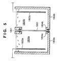
- Fig. 5 is a view showing the arrangement of an anodizing apparatus for manufacturing porous silicon by anodizing a silicon substrate, disclosed in Japanese Patent Laid-Open No. 60-94737.
- This anodizing apparatus is constituted by arranging anodizing tanks 1802a and 1802b consisting of Teflon (trade mark of du Pont in U.S.A) having an HF resistance to sandwich a silicon substrate 1801.
- the anodizing tanks 1802a and 1802b have platinum electrodes 1803a and 1803b, respectively.
- the anodizing tanks 1802a and 1802b have grooves in side walls contacting the silicon substrate 1801, and O-rings 1804a and 1804b of fluororubber are fitted in these grooves, respectively.
- the anodizing tanks 1802a and 1802b and the silicon substrate 1801 are sealed by the O-rings 1804a and 1804b, respectively.
- the sealed anodizing tanks 1802a and 1802b are filled with HF solutions 1805a and 1805b, respectively.
- the silicon substrate does not come into direct contact with the metal electrodes and is hardly contaminated by the metal electrodes.
- the silicon substrate to be anodized is sealed by the O-rings on its upper and lower surfaces, unanodized portions remain in the peripheral regions on the surfaces of the silicon substrate.
- the silicon substrate to be processed itself is directly set and integrated with the anodizing tanks, the silicon substrate cannot be quickly exchanged.
- an anodizing apparatus which supports a silicon substrate at its side surface (beveling) regions has been developed (Japanese Patent Laid-Open No. 5-198556).
- This anodizing apparatus can anodize all surface regions of the substrate while preventing contamination from the metal electrode.
- a wafer to be processed is fixed in a holder, and the holder is fixed in the anodizing tanks, i.e., the wafer is fixed in the anodizing tank in two steps, operability is largely improved as compared to the conventional apparatus which directly fixes a wafer in the anodizing tank to integrate the wafer with the anodizing tank.
- the anodizing apparatuses disclosed in Japanese Patent Laid-Open Nos. 5-198556, 5-86876, and 6-171076 are very practical because metal contamination rarely occurs, and all surface regions of a substrate can be anodized.
- the silicon substrate arranged between the silicon substrate to be processed and the metal electrode is anodized.
- the silicon substrate must be discarded because it is in direct contact with the metal electrode or is contaminated by the metal component dissolved in the electrolytic solution, so the silicon material is wasted.
- the intermediate substrate is also dipped in the electrolytic solution and anodized. Hence, the intermediate substrate must be frequently exchanged, and the silicon material is wasted.
- the present invention has been made to solve the above problems, and has as its object to provide an anodizing apparatus and method capable of efficiently performing anodizing while preventing wafer contamination.
- an anodizing apparatus has the following arrangement.
- anodizing apparatus for anodizing a substrate to be processed in an electrolytic solution, comprising a process tank for storing the electrolytic solution, the process tank having an opening in a wall, a negative electrode arranged in the process tank to oppose the opening, and a positive electrode contacting a surface of the substrate to be processed which is arranged to close the opening from an inside of the process tank, the surface being open outside the process tank through the opening.
- a porous substrate according to the first aspect of the present invention has the following arrangement.
- An anodizing method according to the present invention has the following steps.
- anodizing method of anodizing a substrate to be processed in an electrolytic solution comprising the setting step of setting the substrate to be processed inside a process tank having an opening on a wall to close the opening, the supply step of supplying the electrolytic solution into the process tank, the contacting step of bringing a positive electrode into contact with a portion of the substrate to be processed, which is open outside the process tank through the opening, and the process step of flowing a current between the positive electrode and a negative electrode arranged to oppose the substrate to be processed in the process tank to anodize the substrate to be processed.
- a porous substrate according to the second aspect of the present invention has the following structure.
- porous substrate manufactured by the anodizing method of any one of claims 16 to 27.
- An anodizing apparatus according to an embodiment of the present invention will be described below. Before the description, an embodiment of a method of manufacturing a semiconductor substrate using the anodizing apparatus in some steps will be described.
- Figs. 1A to 1F are views showing a method of manufacturing a semiconductor substrate. This will be briefly described.
- a first substrate prepared by forming a porous silicon layer on a single-crystal silicon substrate, a non-porous layer on the porous silicon layer, and preferably an insulating film on the non-porous layer is bonded to an independently prepared second substrate via the insulating film.
- the single-crystal silicon substrate is removed from the lower surface of the first substrate, and the porous silicon layer is etched, thereby manufacturing a semiconductor substrate.
- a single-crystal Si substrate 51 for forming a first substrate is prepared, and a porous Si layer 52 is formed on the major surface (Fig. 1A).
- the porous Si layer 52 can be formed by processing the major surface of the single-crystal substrate 51 by the anodizing apparatus of the embodiment to be described later.
- At least one non-porous layer 53 is formed on the porous Si layer 52 (Fig. 1B).
- the non-porous layer 53 a single-crystal Si layer, a poly-Si layer, an amorphous Si layer, a metal layer, a semiconductor compound layer, a superconductor layer is suitable.
- a device structure such as a MOSFET may be formed in the non-porous layer 53.
- An SiO 2 layer 54 is formed on the non-porous layer 53, and the resultant structure is preferably used as the first substrate (Fig. 1C).
- This SiO 2 layer 54 is applicable because when the first substrate is bonded to a second substrate 55 in the subsequent step, the interface level of the bonding interface can be separated from the active layer.
- the first substrate is brought into contact with the second substrate 55 at room temperature via the SiO 2 layer 54 (Fig. 1D).
- anode bonding, pressing, heat treatment as needed, or a combination thereof may performed to firmly bond the substrates.
- the first substrate is preferably bonded to the second substrate 55 after the SiO 2 layer 54 is formed on the surface of the single-crystal Si layer by, e.g., thermal oxidation.
- an Si substrate As the second substrate 55, an Si substrate, a substrate obtained by forming an SiO 2 layer on an Si substrate, a transparent substrate consisting of silica glass, or a sapphire substrate is suitable. Any other substrate can be used as far as the second substrate 55 has a sufficiently flat surface to be bonded.
- Fig. 1D shows a state wherein the first substrate and the second substrate are bonded via the SiO 2 layer 54. If the non-porous layer 53 or the second substrate does not consist of Si, the SiO 2 layer 54 need not be formed.
- an insulating thin plate may be inserted between the first substrate and the second substrate.
- the first substrate is removed from the second substrate at the porous Si layer 52 (Fig. 1E).
- the first method using grinding, polishing, or etching (the first substrate is discarded) or the second method of separating the first substrate from the second substrate at the porous layer 52 is used.
- the second method when the porous Si layer remaining on the separated first substrate is removed, and the surface is planarized as needed, the substrate can be reused.
- Fig. 1F schematically shows a semiconductor substrate obtained by the above manufacturing method.
- the non-porous layer 53 e.g., a single-crystal Si layer
- the non-porous layer 53 is formed flat and uniformly in the entire region on the surface of the second substrate 55.
- the semiconductor substrate obtained by the above manufacturing method is very applicable to form an insulated electronic device.
- Formation of a porous silicon substrate by anodizing or formation of pores is performed in, e.g., an HF solution. It is known that the presence of holes is essential for this processing, and the reaction mechanism is estimated as follows.
- a field distribution (field concentration) for preferentially attracting holes is generated at this portion. This surface heterogeneity extends, so etching of silicon atoms continuously progresses along the electric field.
- the solution used for anodizing is not limited to the HF solution, and any other electrolytic solution can be used.
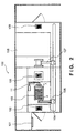
- Fig. 2 is a plan view showing the overall arrangement of the anodizing apparatus of this embodiment.
- an anodizing apparatus 100 is controlled by, e.g., a computer.
- Reference numeral 101 denotes a control panel.
- the loader 102 transfers the substrate to a single substrate conveyor robot 104.
- the wafer conveyor robot 104 removes substrates from the loader 102 one by one, conveys the substrate to an anodizing tank 103, and transfers the substrate to a robot 105.
- the robot 105 causes a holder in the anodizing tank 103 to chuck the received substrate.
- the anodizing tank 103 can simultaneously support seven substrates.
- a positive electrode 11 moves in a direction indicated by an arrow A (details will be described later) and comes into contact with the seventh substrate.
- the anodizing tank 103 is filled with an electrolytic solution, and a voltage is applied across the positive electrode 11 and a negative electrode 2 arranged in the anodizing tank 103, thereby performing anodizing.
- the anodized substrate is removed from the anodizing tank 103 by the robot 105, mounted on a carrier in a washing tank 106, and washed.
- the substrate is conveyed to a drier 108 by a carrier conveyor robot 107 together with the carrier.
- the substrate is conveyed by the carrier conveyor robot 107 again together with the carrier and transferred to an unloader 109 for unloading the substrate.
- Fig. 3 is an enlarged sectional view showing the anodizing tank 103 in Fig. 2.
- the anodizing tank 103 can store seven silicon substrates in fact, though Fig. 3 shows a simple structure for storing two silicon substrates for the descriptive convenience.
- reference numerals 6 and 7 denote single-crystal silicon substrates (wafers).
- a p-type silicon substrate is suitable.
- an n-type silicon substrate can be used by prompting generation of holes by light irradiation or the like.
- the positive electrode 11 and negative electrode 2 are preferably formed from a chemically stable platinum material.
- the positive electrode 11 and negative electrode 2 are connected to a power supply 4.
- a conductive partition 10 is fixed to the positive electrode 11.
- the positive electrode 11 contacts the silicon substrate 7 via the conductive partition 10.
- the conductive partition 10 prevents the silicon substrate from being contaminated by the electrode material when the positive electrode 11 comes into direct contact with the silicon substrate 7.
- a silicon substrate of the same material as that of the silicon substrate 7 to be anodized is used. It is supposed that when the substrates are made of the same silicon material, the silicon substrate 7 to be processed is not contaminated by the silicon material of the conductive partition 10.
- the conductive partition 10 is preferably formed from a material having a low resistivity not to impede current flow from the positive electrode 11 to the silicon substrate 7. In this sense, silicon is a preferable material. However, any material other than silicon can be used as the material of the conductive partition 10 as far as it has a low resistivity and does not contaminate the silicon substrate 7 to be processed.
- a plurality of holes having a diameter of about 5 mm or less are formed in the platinum plate forming the positive electrode 11, and these holes are filled with an adhesive to directly bond the conductive partition 10 to a supporter 14 of the positive electrode 11.
- the conductive partition 10 may be vacuum-chucked using these holes.
- the conductive partition 10 and positive electrode 11 preferably have the same area. However, the diameter of the positive electrode 11 may be smaller than the conductive partition 10 by about 20 mm.
- the conductive partition 10 preferably has a thickness similar to that of the silicon substrate 7 to be processed in fact because when the conductive partition 10 is thin, the field distribution becomes nonuniform, and when the conductive partition 10 is thick, the electrical resistance increases.
- the sizes of the conductive partition 10 and positive electrode 11 are preferably as close to the silicon substrate 7 to be processed as possible.
- the positive electrode 11 is driven in a direction indicated by an arrow B by a driving source 15 such as an air cylinder or a plunger.
- the positive electrode 11 is moved to a position where the positive electrode 11 comes into contact with the silicon substrate 7 and a position separated from the silicon substrate 7.
- a compression spring 17 is inserted between a shaft 16 of the driving source 15 and the supporter 14. When the shaft 16 projects from the driving source 15, the positive electrode 11 is pressed against the silicon substrate 7 by the biasing force of the compression spring 17.
- the biasing force of the compression spring 17 is set not to deform the silicon substrate 7.
- a signal for causing the driving source 15 to project the shaft 16 is detected to determine that the positive electrode 11 is in contact with the silicon substrate 7, or a current is actually flowed between the positive electrode 11 and the negative electrode 2 after supply of an electrolytic solution (HF) 3 into the anodizing tank 103, and electrical connection between the positive electrode 11 and the negative electrode 2 is detected for determination.
- HF electrolytic solution
- Holders 5 for supporting the silicon substrates 6 and 7 are made of, e.g., ethylene tetrafluoride (tradename: Teflon) or a material having HF resistance.
- the holder 5 has an opening having a circle or circular shape and a diameter smaller than that of the silicon substrate to be supported (a circular shape includes a shape close to a circle hereinafter).
- An annular groove is formed at the peripheral portion of the opening of each holder 5, and an O-ring 8 having HF resistance is fitted in this groove. Air is exhausted from a hole (not shown) formed at the bottom portion of this groove, thereby chucking and fixing the silicon substrate 6 or 7 on the holder 5 via the O-ring 8.
- the holder 5 also has, at its lower portion, a seal member 9 for isolating the electrolytic solution 3.
- Chambers 20, 21, 22 of an anodizing tank main body 1 are completely isolated by the O-rings 8 and seal members 9 via the silicon substrates 6 and 7.
- the electrolytic solution 3 supplied to the two chambers 20 and 21 of the anodizing tank main body 1 does not leak to the chamber 22 located at the right end of the anodizing tank main body 1. Since the conductive partition 10 neither contacts the electrolytic solution 3 nor is anodized, the conductive partition 10 need not be exchanged for a long time, so the silicon material is prevented from being wasted.
- a carrier on which silicon substrates are mounted is set in the loader 102 (step S2).
- Each silicon substrate is conveyed from the loader 102 to the anodizing tank 103 by the robots 104 and 105 until seven silicon substrates are chucked by the holder 5 (steps S4 to S10).
- the driving source 15 is driven to bring the positive electrode 11 into contact with the silicon substrate 7 via the conductive partition 10 (step S12).
- the electrolytic solution 3 is supplied to the anodizing tank 103 and circulated, and the power supply 4 is turned on to perform anodizing (steps S14 to S18).
- the electrolytic solution is discharged from a discharge port (not shown) formed in the anodizing tank 103, and pure water is supplied to the anodizing tank 103 (steps S20 to S22). With this operation, the silicon substrates are roughly cleaned.
- the pure water is discharged from the anodizing tank 103, and the positive electrode 11 is separated from the silicon substrate 7 (steps S24 to S26).
- each silicon substrate is released and moved to a carrier in the washing tank 106. This operation is repeatedly performed for the seven silicon substrates (steps S28 to S34).
- step S36 it is determined whether silicon substrates remain on the carrier on the loader. If any silicon substrates remain, the process from step S4 to step S36 is repeated. If it is determined in step S36 that no silicon substrate remains on the carrier on the loader 102, anodizing of 25 silicon substrates is complete, so 25 anodized silicon substrates are stored on the carrier in the washing tank 106.
- the anodized silicon substrates are washed, and the washed silicon substrates are conveyed to the drier 108 by the robot 107 together with the carrier and dried (steps S38 to S42).
- the dried silicon substrates are conveyed to the unloader 109 by the robot 107 together with the carrier and unloaded (step S44).
- the empty carrier is set in the unloader 109, conveyed to the washing tank 106 by the robot 107, and sank in the washing tank 106.
- step S2 a carrier storing new silicon substrates is set in the loader 102, and the operation from step S2 to step S50 is repeated.
- step S50 If it is determined in step S50 that no carriers storing new silicon substrates remain, the operation of the apparatus is ended.
- the conductive partition 10 for preventing contamination of the silicon substrate is inserted between the positive electrode 11 and the silicon substrate 7, contamination of the silicon substrate due to the electrode material can be prevented.
- the conductive partition 10 is not anodized and can be repeatedly used, so the silicon material can be prevented from being wasted.
- an anodizing apparatus and method capable of efficiently performing anodizing while preventing wafer contamination are provided.
Landscapes
- Chemical & Material Sciences (AREA)
- Organic Chemistry (AREA)
- Chemical Kinetics & Catalysis (AREA)
- Electrochemistry (AREA)
- Materials Engineering (AREA)
- Metallurgy (AREA)
- Engineering & Computer Science (AREA)
- Life Sciences & Earth Sciences (AREA)
- Sustainable Development (AREA)
- Weting (AREA)
- Formation Of Insulating Films (AREA)
- Immobilizing And Processing Of Enzymes And Microorganisms (AREA)
- Cleaning Or Drying Semiconductors (AREA)
Applications Claiming Priority (2)
| Application Number | Priority Date | Filing Date | Title |
|---|---|---|---|
| JP36101397A JP3413090B2 (ja) | 1997-12-26 | 1997-12-26 | 陽極化成装置及び陽極化成処理方法 |
| JP36101397 | 1997-12-26 |
Publications (3)
| Publication Number | Publication Date |
|---|---|
| EP0926269A2 true EP0926269A2 (de) | 1999-06-30 |
| EP0926269A3 EP0926269A3 (de) | 2000-05-31 |
| EP0926269B1 EP0926269B1 (de) | 2003-08-20 |
Family
ID=18471827
Family Applications (1)
| Application Number | Title | Priority Date | Filing Date |
|---|---|---|---|
| EP98310455A Expired - Lifetime EP0926269B1 (de) | 1997-12-26 | 1998-12-18 | Vorrichtung zur anodischen Oxidation und Verfahren und poröses Substrat |
Country Status (10)
| Country | Link |
|---|---|
| US (1) | US6258240B1 (de) |
| EP (1) | EP0926269B1 (de) |
| JP (1) | JP3413090B2 (de) |
| KR (1) | KR100369731B1 (de) |
| CN (1) | CN1092720C (de) |
| AT (1) | ATE247727T1 (de) |
| AU (1) | AU741464B2 (de) |
| DE (1) | DE69817308T2 (de) |
| SG (1) | SG71181A1 (de) |
| TW (1) | TW540116B (de) |
Cited By (1)
| Publication number | Priority date | Publication date | Assignee | Title |
|---|---|---|---|---|
| EP1039508A3 (de) * | 1999-03-25 | 2005-07-06 | Canon Kabushiki Kaisha | Vorrichtung und System zur anodischen Oxidation, Vorrichtung und Verfahren zur Bearbeitung von Substraten, und Substratherstellungsverfahren |
Families Citing this family (7)
| Publication number | Priority date | Publication date | Assignee | Title |
|---|---|---|---|---|
| KR100453454B1 (ko) * | 2001-01-09 | 2004-10-15 | 텔레포스 주식회사 | 양극화 반응 장치 및 단위 양극화 반응기 |
| US20040124088A1 (en) * | 2002-12-26 | 2004-07-01 | Canon Kabushiki Kaisha | Processing apparatus |
| KR100854576B1 (ko) * | 2007-05-16 | 2008-08-26 | 주식회사 동부하이텍 | 반도체 소자의 세정 장치 및 반도체 소자의 세정 방법 |
| KR100897259B1 (ko) * | 2007-10-24 | 2009-05-14 | 공주대학교 산학협력단 | 다중조건 다공질 규소층의 제작 방법 |
| JP5908266B2 (ja) * | 2011-11-30 | 2016-04-26 | 株式会社Screenホールディングス | 陽極化成装置及びそれを備えた陽極化成システム並びに半導体ウエハ |
| WO2016094271A1 (en) * | 2014-12-10 | 2016-06-16 | Applied Materials, Inc. | System and method for all wrap around porous silicon formation |
| JPWO2024219268A1 (de) * | 2023-04-18 | 2024-10-24 |
Family Cites Families (15)
| Publication number | Priority date | Publication date | Assignee | Title |
|---|---|---|---|---|
| US3345274A (en) * | 1964-04-22 | 1967-10-03 | Westinghouse Electric Corp | Method of making oxide film patterns |
| US4069121A (en) * | 1975-06-27 | 1978-01-17 | Thomson-Csf | Method for producing microscopic passages in a semiconductor body for electron-multiplication applications |
| JPS57126998A (en) * | 1981-01-28 | 1982-08-06 | Mishima Kosan Co Ltd | Plating apparatus |
| JPS6094737A (ja) | 1983-10-28 | 1985-05-27 | Matsushita Electric Works Ltd | 半導体装置の製法 |
| FR2615036B1 (fr) | 1987-05-05 | 1989-08-18 | France Etat | Machine pour la fabrication de silicium poreux |
| JP2608351B2 (ja) | 1990-08-03 | 1997-05-07 | キヤノン株式会社 | 半導体部材及び半導体部材の製造方法 |
| JP2734269B2 (ja) * | 1991-12-26 | 1998-03-30 | 日本電気株式会社 | 半導体製造装置 |
| JPH0613366A (ja) | 1992-04-03 | 1994-01-21 | Internatl Business Mach Corp <Ibm> | 多孔性シリコン膜およびデバイスを作成するための浸漬走査方法およびシステム |
| JPH0631488A (ja) * | 1992-07-14 | 1994-02-08 | Matsushita Electric Ind Co Ltd | 溶接用位置決め治具 |
| JP3201875B2 (ja) | 1993-04-27 | 2001-08-27 | キヤノン株式会社 | 陽極化成装置及び陽極化成法 |
| DE69312636T2 (de) | 1992-11-09 | 1998-02-05 | Canon Kk | Anodisierungsapparat mit einer Trägervorrichtung für das zu behandelnde Substrat |
| JP3416190B2 (ja) | 1993-03-23 | 2003-06-16 | キヤノン株式会社 | 陽極化成装置及び陽極化成方法 |
| JPH06338631A (ja) | 1993-03-29 | 1994-12-06 | Canon Inc | 発光素子及びその製造方法 |
| JPH0837173A (ja) | 1994-07-22 | 1996-02-06 | Canon Inc | 化成装置 |
| JP3376258B2 (ja) | 1996-11-28 | 2003-02-10 | キヤノン株式会社 | 陽極化成装置及びそれに関連する装置及び方法 |
-
1997
- 1997-12-26 JP JP36101397A patent/JP3413090B2/ja not_active Expired - Fee Related
-
1998
- 1998-12-15 US US09/211,418 patent/US6258240B1/en not_active Expired - Lifetime
- 1998-12-15 SG SG1998005840A patent/SG71181A1/en unknown
- 1998-12-16 TW TW087120971A patent/TW540116B/zh active
- 1998-12-18 DE DE69817308T patent/DE69817308T2/de not_active Expired - Fee Related
- 1998-12-18 AT AT98310455T patent/ATE247727T1/de not_active IP Right Cessation
- 1998-12-18 EP EP98310455A patent/EP0926269B1/de not_active Expired - Lifetime
- 1998-12-24 AU AU98183/98A patent/AU741464B2/en not_active Ceased
- 1998-12-25 CN CN98125517A patent/CN1092720C/zh not_active Expired - Fee Related
- 1998-12-26 KR KR10-1998-0058985A patent/KR100369731B1/ko not_active Expired - Fee Related
Cited By (2)
| Publication number | Priority date | Publication date | Assignee | Title |
|---|---|---|---|---|
| EP1039508A3 (de) * | 1999-03-25 | 2005-07-06 | Canon Kabushiki Kaisha | Vorrichtung und System zur anodischen Oxidation, Vorrichtung und Verfahren zur Bearbeitung von Substraten, und Substratherstellungsverfahren |
| US7014748B2 (en) | 1999-03-25 | 2006-03-21 | Canon Kabushiki Kaisha | Anodizing method, substrate processing method, and substrate manufacturing method |
Also Published As
| Publication number | Publication date |
|---|---|
| AU9818398A (en) | 1999-07-15 |
| AU741464B2 (en) | 2001-11-29 |
| JP3413090B2 (ja) | 2003-06-03 |
| JPH11195640A (ja) | 1999-07-21 |
| SG71181A1 (en) | 2000-03-21 |
| TW540116B (en) | 2003-07-01 |
| DE69817308T2 (de) | 2004-06-17 |
| US6258240B1 (en) | 2001-07-10 |
| EP0926269A3 (de) | 2000-05-31 |
| CN1092720C (zh) | 2002-10-16 |
| KR19990063513A (ko) | 1999-07-26 |
| ATE247727T1 (de) | 2003-09-15 |
| EP0926269B1 (de) | 2003-08-20 |
| CN1227284A (zh) | 1999-09-01 |
| KR100369731B1 (ko) | 2003-03-17 |
| DE69817308D1 (de) | 2003-09-25 |
Similar Documents
| Publication | Publication Date | Title |
|---|---|---|
| US6517697B1 (en) | Anodizing method | |
| US6200878B1 (en) | SOI substrate processing method | |
| US6547938B1 (en) | Anodizing apparatus, utilizing a perforated negative electrode | |
| TW487984B (en) | Method of cleaning porous body and process for producing porous body, non-porous film or bonded substrate | |
| EP0940483A2 (de) | Anodisierungsverfahren und Vorrichtung und Verfahren zur Herstellung eines Halbleitersubstrats | |
| EP0926269B1 (de) | Vorrichtung zur anodischen Oxidation und Verfahren und poröses Substrat | |
| JP4598413B2 (ja) | 貼り合わせウエーハの製造方法及び貼り合わせウエーハの酸化膜除去用治具 | |
| JP3342381B2 (ja) | 陽極化成装置 | |
| JP2000277484A (ja) | 陽極化成装置、陽極化成用電極、基板の処理方法及び基板の製造方法 | |
| AU749905B2 (en) | Anodizing apparatus and apparatus and method associated with the same | |
| JP2004103800A (ja) | 陽極化成装置及び陽極化成方法、基板製造方法、並びに、基板処理装置及び基板処理方法 | |
| JP2004099965A (ja) | 陽極化成装置及び陽極化成方法、基板製造方法、並びに、基板処理装置及び基板処理方法 |
Legal Events
| Date | Code | Title | Description |
|---|---|---|---|
| PUAI | Public reference made under article 153(3) epc to a published international application that has entered the european phase |
Free format text: ORIGINAL CODE: 0009012 |
|
| AK | Designated contracting states |
Kind code of ref document: A2 Designated state(s): AT BE DE ES FR GB IT NL SE |
|
| AX | Request for extension of the european patent |
Free format text: AL;LT;LV;MK;RO;SI |
|
| PUAL | Search report despatched |
Free format text: ORIGINAL CODE: 0009013 |
|
| AK | Designated contracting states |
Kind code of ref document: A3 Designated state(s): AT BE CH CY DE DK ES FI FR GB GR IE IT LI LU MC NL PT SE |
|
| AX | Request for extension of the european patent |
Free format text: AL;LT;LV;MK;RO;SI |
|
| 17P | Request for examination filed |
Effective date: 20001020 |
|
| AKX | Designation fees paid |
Free format text: AT BE DE ES FR GB IT NL SE |
|
| 17Q | First examination report despatched |
Effective date: 20010221 |
|
| GRAH | Despatch of communication of intention to grant a patent |
Free format text: ORIGINAL CODE: EPIDOS IGRA |
|
| GRAH | Despatch of communication of intention to grant a patent |
Free format text: ORIGINAL CODE: EPIDOS IGRA |
|
| GRAA | (expected) grant |
Free format text: ORIGINAL CODE: 0009210 |
|
| AK | Designated contracting states |
Designated state(s): AT BE DE ES FR GB IT NL SE |
|
| PG25 | Lapsed in a contracting state [announced via postgrant information from national office to epo] |
Ref country code: NL Free format text: LAPSE BECAUSE OF FAILURE TO SUBMIT A TRANSLATION OF THE DESCRIPTION OR TO PAY THE FEE WITHIN THE PRESCRIBED TIME-LIMIT Effective date: 20030820 Ref country code: BE Free format text: LAPSE BECAUSE OF FAILURE TO SUBMIT A TRANSLATION OF THE DESCRIPTION OR TO PAY THE FEE WITHIN THE PRESCRIBED TIME-LIMIT Effective date: 20030820 Ref country code: AT Free format text: LAPSE BECAUSE OF FAILURE TO SUBMIT A TRANSLATION OF THE DESCRIPTION OR TO PAY THE FEE WITHIN THE PRESCRIBED TIME-LIMIT Effective date: 20030820 |
|
| REG | Reference to a national code |
Ref country code: GB Ref legal event code: FG4D |
|
| REF | Corresponds to: |
Ref document number: 69817308 Country of ref document: DE Date of ref document: 20030925 Kind code of ref document: P |
|
| PG25 | Lapsed in a contracting state [announced via postgrant information from national office to epo] |
Ref country code: SE Free format text: LAPSE BECAUSE OF FAILURE TO SUBMIT A TRANSLATION OF THE DESCRIPTION OR TO PAY THE FEE WITHIN THE PRESCRIBED TIME-LIMIT Effective date: 20031120 |
|
| PG25 | Lapsed in a contracting state [announced via postgrant information from national office to epo] |
Ref country code: ES Free format text: LAPSE BECAUSE OF FAILURE TO SUBMIT A TRANSLATION OF THE DESCRIPTION OR TO PAY THE FEE WITHIN THE PRESCRIBED TIME-LIMIT Effective date: 20031201 |
|
| NLV1 | Nl: lapsed or annulled due to failure to fulfill the requirements of art. 29p and 29m of the patents act | ||
| ET | Fr: translation filed | ||
| PLBE | No opposition filed within time limit |
Free format text: ORIGINAL CODE: 0009261 |
|
| STAA | Information on the status of an ep patent application or granted ep patent |
Free format text: STATUS: NO OPPOSITION FILED WITHIN TIME LIMIT |
|
| 26N | No opposition filed |
Effective date: 20040524 |
|
| PGFP | Annual fee paid to national office [announced via postgrant information from national office to epo] |
Ref country code: IT Payment date: 20081211 Year of fee payment: 11 |
|
| PGFP | Annual fee paid to national office [announced via postgrant information from national office to epo] |
Ref country code: DE Payment date: 20081231 Year of fee payment: 11 |
|
| PGFP | Annual fee paid to national office [announced via postgrant information from national office to epo] |
Ref country code: GB Payment date: 20081224 Year of fee payment: 11 |
|
| PGFP | Annual fee paid to national office [announced via postgrant information from national office to epo] |
Ref country code: FR Payment date: 20081222 Year of fee payment: 11 |
|
| GBPC | Gb: european patent ceased through non-payment of renewal fee |
Effective date: 20091218 |
|
| REG | Reference to a national code |
Ref country code: FR Ref legal event code: ST Effective date: 20100831 |
|
| PG25 | Lapsed in a contracting state [announced via postgrant information from national office to epo] |
Ref country code: FR Free format text: LAPSE BECAUSE OF NON-PAYMENT OF DUE FEES Effective date: 20091231 |
|
| PG25 | Lapsed in a contracting state [announced via postgrant information from national office to epo] |
Ref country code: DE Free format text: LAPSE BECAUSE OF NON-PAYMENT OF DUE FEES Effective date: 20100701 |
|
| PG25 | Lapsed in a contracting state [announced via postgrant information from national office to epo] |
Ref country code: GB Free format text: LAPSE BECAUSE OF NON-PAYMENT OF DUE FEES Effective date: 20091218 |
|
| PG25 | Lapsed in a contracting state [announced via postgrant information from national office to epo] |
Ref country code: IT Free format text: LAPSE BECAUSE OF NON-PAYMENT OF DUE FEES Effective date: 20091218 |