EP0926724A2 - Strukturierung von porösem Silizium mittels einer Silizumkarbid-Maske - Google Patents
Strukturierung von porösem Silizium mittels einer Silizumkarbid-Maske Download PDFInfo
- Publication number
- EP0926724A2 EP0926724A2 EP98204296A EP98204296A EP0926724A2 EP 0926724 A2 EP0926724 A2 EP 0926724A2 EP 98204296 A EP98204296 A EP 98204296A EP 98204296 A EP98204296 A EP 98204296A EP 0926724 A2 EP0926724 A2 EP 0926724A2
- Authority
- EP
- European Patent Office
- Prior art keywords
- range
- order
- etching
- sccm
- silicon carbide
- Prior art date
- Legal status (The legal status is an assumption and is not a legal conclusion. Google has not performed a legal analysis and makes no representation as to the accuracy of the status listed.)
- Granted
Links
Images


Classifications
-
- H—ELECTRICITY
- H10—SEMICONDUCTOR DEVICES; ELECTRIC SOLID-STATE DEVICES NOT OTHERWISE PROVIDED FOR
- H10W—GENERIC PACKAGES, INTERCONNECTIONS, CONNECTORS OR OTHER CONSTRUCTIONAL DETAILS OF DEVICES COVERED BY CLASS H10
- H10W10/00—Isolation regions in semiconductor bodies between components of integrated devices
-
- H—ELECTRICITY
- H10—SEMICONDUCTOR DEVICES; ELECTRIC SOLID-STATE DEVICES NOT OTHERWISE PROVIDED FOR
- H10P—GENERIC PROCESSES OR APPARATUS FOR THE MANUFACTURE OR TREATMENT OF DEVICES COVERED BY CLASS H10
- H10P50/00—Etching of wafers, substrates or parts of devices
- H10P50/69—Etching of wafers, substrates or parts of devices using masks for semiconductor materials
- H10P50/691—Etching of wafers, substrates or parts of devices using masks for semiconductor materials for Group V materials or Group III-V materials
- H10P50/692—Etching of wafers, substrates or parts of devices using masks for semiconductor materials for Group V materials or Group III-V materials characterised by their composition, e.g. multilayer masks or materials
-
- H—ELECTRICITY
- H10—SEMICONDUCTOR DEVICES; ELECTRIC SOLID-STATE DEVICES NOT OTHERWISE PROVIDED FOR
- H10W—GENERIC PACKAGES, INTERCONNECTIONS, CONNECTORS OR OTHER CONSTRUCTIONAL DETAILS OF DEVICES COVERED BY CLASS H10
- H10W10/00—Isolation regions in semiconductor bodies between components of integrated devices
- H10W10/01—Manufacture or treatment
-
- H—ELECTRICITY
- H10—SEMICONDUCTOR DEVICES; ELECTRIC SOLID-STATE DEVICES NOT OTHERWISE PROVIDED FOR
- H10W—GENERIC PACKAGES, INTERCONNECTIONS, CONNECTORS OR OTHER CONSTRUCTIONAL DETAILS OF DEVICES COVERED BY CLASS H10
- H10W10/00—Isolation regions in semiconductor bodies between components of integrated devices
- H10W10/01—Manufacture or treatment
- H10W10/011—Manufacture or treatment of isolation regions comprising dielectric materials
-
- H—ELECTRICITY
- H10—SEMICONDUCTOR DEVICES; ELECTRIC SOLID-STATE DEVICES NOT OTHERWISE PROVIDED FOR
- H10W—GENERIC PACKAGES, INTERCONNECTIONS, CONNECTORS OR OTHER CONSTRUCTIONAL DETAILS OF DEVICES COVERED BY CLASS H10
- H10W10/00—Isolation regions in semiconductor bodies between components of integrated devices
- H10W10/01—Manufacture or treatment
- H10W10/011—Manufacture or treatment of isolation regions comprising dielectric materials
- H10W10/012—Manufacture or treatment of isolation regions comprising dielectric materials using local oxidation of silicon [LOCOS]
-
- H—ELECTRICITY
- H10—SEMICONDUCTOR DEVICES; ELECTRIC SOLID-STATE DEVICES NOT OTHERWISE PROVIDED FOR
- H10W—GENERIC PACKAGES, INTERCONNECTIONS, CONNECTORS OR OTHER CONSTRUCTIONAL DETAILS OF DEVICES COVERED BY CLASS H10
- H10W10/00—Isolation regions in semiconductor bodies between components of integrated devices
- H10W10/10—Isolation regions comprising dielectric materials
-
- H—ELECTRICITY
- H10—SEMICONDUCTOR DEVICES; ELECTRIC SOLID-STATE DEVICES NOT OTHERWISE PROVIDED FOR
- H10W—GENERIC PACKAGES, INTERCONNECTIONS, CONNECTORS OR OTHER CONSTRUCTIONAL DETAILS OF DEVICES COVERED BY CLASS H10
- H10W10/00—Isolation regions in semiconductor bodies between components of integrated devices
- H10W10/10—Isolation regions comprising dielectric materials
- H10W10/13—Isolation regions comprising dielectric materials formed using local oxidation of silicon [LOCOS], e.g. sealed interface localised oxidation [SILO] or side-wall mask isolation [SWAMI]
-
- H—ELECTRICITY
- H10—SEMICONDUCTOR DEVICES; ELECTRIC SOLID-STATE DEVICES NOT OTHERWISE PROVIDED FOR
- H10D—INORGANIC ELECTRIC SEMICONDUCTOR DEVICES
- H10D62/00—Semiconductor bodies, or regions thereof, of devices having potential barriers
- H10D62/80—Semiconductor bodies, or regions thereof, of devices having potential barriers characterised by the materials
- H10D62/83—Semiconductor bodies, or regions thereof, of devices having potential barriers characterised by the materials being Group IV materials, e.g. B-doped Si or undoped Ge
- H10D62/832—Semiconductor bodies, or regions thereof, of devices having potential barriers characterised by the materials being Group IV materials, e.g. B-doped Si or undoped Ge being Group IV materials comprising two or more elements, e.g. SiGe
- H10D62/8325—Silicon carbide
Definitions
- the invention is generally related to the field of forming porous silicon areas in semiconductor devices and more specifically to patterning techniques for forming such porous silicon areas.
- Porous silicon has a low dielectric constant and high resistivity which make it useful for various applications. Some reported applications include: isolation of power devices from other circuitry and optoelectronics/photoluminesence.
- PS is formed by anodic oxidation of a silicon wafer in a solution of hydrofluoric acid and methanol. Uniform, thick (100 ⁇ m) films having a specular surface can be produced in 15 minutes.
- the PS film structure consists of interconnected pores in a single crystal silicon matrix which retains the orientation of the silicon wafer. The pore fraction is a function of the anodization conditions and typically ranges from 30% to 50%.
- the pore structure of PS is determined by the doping level of the starting silicon wafer.
- the structure In degeneratively doped n-type or p-type silicon, the structure consists of many long pores running perpendicular to the silicon wafer surface with many small "buds" on the sides of the pores which can result in branching.
- lightly doped n-type or p-type silicon the pore structure consists of an apparently random, interconnected distribution of voids. For a pore fraction of 50%, the size of the pores in lightly doped material is in the 50 ⁇ range, while those in degeneratively doped material are around 150 ⁇ . Once the sidewalls of a pore have formed, they are remarkably resistant to further anodic attack.
- FIG. 1 The construction of a commonly employed chamber is illustrated in FIG. 1.
- the silicon wafer 10 separates the front 12 and rear 14 half cells, each having a platinum electrode 16 and pumped supply of electrolyte 18.
- the PS film forms on the anode side of the wafer; the silicon is cathodic in the back half cell and does not react.
- the most important variables affecting the PS structure are (1) substrate doping type and level; (2) HF concentration (10 - 48%); and (3) current density (typically 1 - 100 mA/cm 2 ).
- substrate doping type and level (2) HF concentration (10 - 48%); and (3) current density (typically 1 - 100 mA/cm 2 ).
- HF concentration typically 1 - 100 mA/cm 2
- current density typically 1 - 100 mA/cm 2
- Porosity generally increases with increasing current density and decreasing HF concentration.
- Porous silicon has a high internal surface area, but the impurities found on these surfaces (oxygen, carbon, fluor
- a method of selectively forming porous silicon regions in a silicon substrate is disclosed herein.
- a layer of SiC is deposited by PECVD over the substrate using a silane/methane, trimethylsilane, tetramethylsilane or other organosilicon precursor gas at a temperature between 200 - 500°C.
- the layer of SiC is then patterned and etched to expose the region of the substrate where porous silicon is desired.
- An anodization process is performed to convert a region of the substrate to porous silicon.
- This provides a low temperature process for selectively forming porous silicon regions, and a masking material that is compatible with the anodization processes and is not removed by the HF used in the anodization process.
- a process is disclosed herein for selectively forming areas of porous silicon in a substrate after the formation of transistors in the substrate. As such, these teachings are believed to be very beneficial for RF (radio frequency) applications by isolating passive RF components from the substrate both in an IC and an integrated Si PC board as will be discussed herein below.
- porous silicon involves a wet anodic etch process in a bath of a very acidic electrolyte.
- the electrolyte is typically a combination of HF, H2O, and a surfactant such as ethanol or methanol.
- the pH level is often less than 1.
- a masking step is necessary to prevent previously grown structures (i.e., transistors) from being removed from the surface during anodization.
- the key aspect of these teachings is in the choice and formation of the masking layer.
- the problem is that typical masking materials such as photoresist and silicon nitride have poor stability in the presence of HF.
- silicon carbide (SiC) is deposited using a new process that is compatible with production-level IC processing.
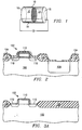
- Fig. 2 shows a cross-section of a substrate 100 having transistors 102 formed therein.
- a masking layer 104 is located over the substrate 100 and transistors 102 except in areas where PS 106 is desired.
- Masking layer 104 comprises an amorphous-SiC:H layer deposited using an organosilicon gas such as silane/methane, trimethylsilane, or tetramethylsilane, PECVD (plasma-enhanced chemical vapor deposition).
- PECVD plasma-enhanced chemical vapor deposition
- Masking layer 104 is carbon rich and a 500 ⁇ thick film can withstand an HF electrolyte environment for at least 18 hrs without observable degradation.
- Substrate temperatures need not exceed 350°C and are typically between 250°C and 350°C depending on the desired film properties.
- the deposition rate is greater than 200 ⁇ /min with good step coverage.
- Film stress can be adjusted from -100 to +200 MPa by varying the ambient pressure.
- a masking layer comprising an amorphous-SiC:H layer deposited using an organosilicon precursor gas PECVD process overcomes problems with other prior art masking materials of withstanding the HF environment and, by using lower deposition temperatures, overcomes process integration problems with prior art SiC deposition processes.
- the SiC masking layer 104 is deposited after the transistor silicide process and is not removed from the regions through which contacts will be made.
- the device is processed through isolation regions 108 and transistor 102 formation.
- Transistors 102 are fabricated through silicide 110 formation and anneal (Ti or W).
- Isolation regions 108 are shown as field oxide regions. However, they may alternatively be another type of isolation such as shallow trench isolation STI. For STI, process through STI planarization and etch the polish stop layer, leaving the underlying oxide layer.
- an optional oxide layer may be deposited at this point.
- This oxide layer may be deposited by, for example, PETEOS or LPCVD TEOS to a thickness on the order of 5000 - 10,000 ⁇ (Angstroms).
- a resist layer 112 is formed over the surface as shown in FIG. 3B.
- the resist layer 112 is patterned as shown in FIG. 3C to expose an area 114 of isolation region 108. Area 114 is located over the desired PS site.
- the oxide of isolation regions 108 is etched leaving sloped sidewalls on the order of 45°, as shown in FIG. 3D. This may, for example, be accomplished in one of the following two ways: (1) isotropic plasma etch using CF 4 /O 2 or its equivalent or (2) HF deglaze. Resist layer 112 is then removed using standard ash/cleanup processes.
- oxide pattern and etch steps may alternatively be performed prior to transistor formation.
- a p+ diffusion of boron or similar dopant may be performed prior to the transistor formation to convert the p- epi to p+ w/resistivity on the order of 0.01 ⁇ -cm. If necessary, a deglaze to remove the boron or similar dopant contaminated oxide is then performed and a pad oxide is re-grown to a thickness on the order of 100-500 ⁇ .
- a masking layer 104 of a-SiC:H is deposited over the structure.
- Layer 104 may typically have a thickness in the range of 1000 ⁇ to 5000 ⁇ .
- the following process may be used: PECVD using silane/methane, trimethylsilane, tetramethylsilane or other organosilicon precursor gas and Ar or He as carrier gas.
- the pressure may be on the order of 5 Torr.
- the gas flow may be in the range of 500-5000 sccm.
- RF power density may be on the order of 2 W/cm 2 (13.56 MHz).
- the substrate temperature may be in the range of 200 - 500 °C. If desired, a double deposition step (using the same conditions) may be used to reduce defects.
- Second resist mask 116 is formed over the SiC masking layer 104.
- Second resist mask 116 exposes a portion 118 of SiC masking layer 104 approximately in the center of where the PS region is desired, as shown in FIG. 3F.
- the exposed portion 118 is significantly smaller than the width of the desired PS region.
- the relationship between the size of portion 118 and the desired PS region is optimized based on the PS formation process parameters.
- the exposed portion 118 of SiC masking layer 104 is removed.
- Methods for removing SiC are known in the art. The following are some exemplary methods for removing portion 118 of SiC masking layer 104.
- Cl 2 based etch [Selectivity of the etch, with this gas, down to the oxide should not be an issue.
- PS regions 106 are formed by anodization, as shown in FIG. 3H.
- the thickness of PS region 106 may vary between 10 ⁇ m and perhaps the wafer thickness, depending on the application.
- PS region 106 may be in the range of 10 - 200 ⁇ m.
- Suitable anodization methods are known in the art.
- the constant porosity may be in the range of 45 - 70% and the current density may be in the range of 30 - 100 mA/cm 2 .
- the electrolyte may be a 49% HF plus a surfactant such as ethanol.
- PS layer 106a may have a thickness in the range of 0.2 - 1 ⁇ m and a porosity in the range of 25 - 40%. This may be accomplished using a current density in the range of 1 - 5 mA/cm 2 .
- PS layer 106b may then have a thickness in the range of 10 ⁇ m to perhaps the wafer thickness thick and a higher porosity in the range of 45 - 70%. This may be accomplished using a current density in the range of 30 - 100 mA/cm 2 .
- the electrolyte may be the same in both cases: 49% HF + surfactant such as ethanol (approximately 50% solution of each).
- the anodization process may be performed while illuminating the back side of the wafers with above bandgap optical radiation. Exposing the wafers to light will reduce the resistivity of the Si.
- PMD 120 is deposited.
- PMD 120 typically comprises a PECVD TEOS.
- other PMD materials known in the art may alternatively be used as well as silicon nitride or SiC. If SiC is used , the process should also be a PECVD using trimethylsilane (or other organosilicon gas) and a Ar or He carrier gas @ ⁇ 5 Torr (gas flow 500-5000 sccm), RF power density -2 W/cm 2 (13.56 MHz), Substrate temp 200 - 500 °C.
- the PMD 120 is then patterned and a contact etch is performed to etch through the PMD 120, SiC masking layer 104 and the optional oxide layer if present down to the silicide 110, as shown in FIG. 3J.
- a multi-step etch is preferably used because an etch that will remove both SiC and SiO 2 will probably have poor selectivity between the dielectrics and the silicide, and most likely cut into the silicide. Without the multistep etch, poor process control may result.
- Processing then continues to form metal interconnect layers and any passive components. In order to be isolated from the substrate, these passive components would be formed over PS regions 106.
- the SiC masking layer 104 is deposited after the transistor silicide process and is removed from the regions through which contacts will be made.
- device is processed through isolation regions 108 and transistor 102 formation.
- Transistors 102 are fabricated through silicide 110 formation and anneal (Ti or W). Isolation regions 108 are shown as field oxide regions. However, there may alternatively be another type of isolation such as shallow trench isolation.
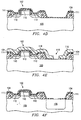
- an oxide layer 111 is deposited as shown in FIG. 4A.
- this oxide layer is not optional and must be present for the removal of SiC later in the process.
- This oxide layer may be deposited by, for example, PETEOS or LPCVD TEOS to a thickness on the order of 1000 ⁇ .
- a resist layer 112 is formed over the surface.
- the resist layer 112 is patterned as shown in FIG. 4B to expose an area 114 of isolation region 108. Area 114 is located over the desired PS site.
- the oxide of isolation regions 108 is etched leaving sloped sidewalls on the order of 45°, as shown in FIG. 4C. This may, for example, be accomplished in one of the following two ways: (1) isotropic plasma etch using CF 4 /O 2 or its equivalent or (2) HF deglaze. Resist layer 112 is then removed using standard ash/cleanup processes.
- a p+ implant/diffusion step is needed prior to transistor formation to convert the p- epi to p+ resistivity on the order of 0.01 ⁇ -cm where porous silicon is desired.
- An deglaze/oxide etch may subsequently be performed to removed the dopant contaminated oxide and a pad oxide may be regrown to a thickness on the order of 100-500 ⁇ .
- a masking layer 104 of a-SiC:H is deposited over the structure.
- Layer 104 may typically have a thickness in the range of 1000 ⁇ to 5000 ⁇ .
- the following process may be used: PECVD using trimethylsilane and Ar or He as carrier gas.
- the pressure may be on the order of 5 Torr.
- the gas flow may be in the range of 500-2000 sccm.
- RF power density may be on the order of 2 W/cm 2 (13.56 MHz).
- the substrate temperature may be in the range of 200 - 500 °C. If desired, a double deposition step (using the same conditions) may be used to reduce defects.
- Second resist mask 116 is formed over the SiC masking layer 104.
- Second resist mask 116 exposes a portion 118 of SiC masking layer 104 approximately in the center of where the PS region is desired, as shown in FIG. 4E.
- the exposed portion 118 is significantly smaller than the width of the desired PS region.
- the relationship between the size of portion 118 and the desired PS region is optimized based on the PS formation process parameters.
- the exposed portion 118 of SiC masking layer 104 is removed.
- Methods for removing SiC are known in the art. The following are some exemplary methods for removing portion 118 of SiC masking layer 104.
- Cl 2 based etch [Selectivity of the etch, with this gas, down to the oxide should not be an issue.
- PS regions 106 are formed by anodization, as shown in FIG. 4F.
- the thickness of PS region 106 may vary between 10 ⁇ m and perhaps the wafer thickness, depending on the application. Typically, PS region 106 may be in the range of 10 - 200 ⁇ m.
- the constant porosity may be in the range of 45 - 70% and the current density may be in the range of 30 - 100 mA/cm 2 .
- the electrolyte may be a 49% HF plus a surfactant such as ethanol.
- PS layer 106a may have a thickness in the range of 0.2 - 1 ⁇ m and a porosity in the range of 25 - 40%. This may be accomplished using a current density in the range of 1 - 5 mA/cm 2 .
- PS layer 106b may then have a thickness in the range of 10 ⁇ m to perhaps the wafer thickness thick and a higher porosity in the range of 45 - 70%. This may be accomplished using a current density in the range of 30 - 100 mA/cm 2 .
- the electrolyte may be the same in both cases: 49% HF + surfactant such as ethanol (approximately 50% solution of each).
- the anodization process may be performed while illuminating the back side of the wafers with above bandgap optical radiation. Exposing the wafers to light will reduce the resistivity of the Si.
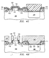
- a capping layer 122 may be deposited over the SiC masking layer 104, as shown in FIG. 4G.
- the capping layer may comprise SiC or silicon nitride and have a thickness on the order of 1500 ⁇ . If SiC is used, the same deposition process should be used as earlier in the process.
- a third resist mask 124 is then formed over capping layer 122 leaving the areas anodized covered and exposing the remaining areas.
- the SiC masking layer 104 and capping layer 122 if present are etched stopping on oxide layer 111. If the optional third resist mask 124 is used, portions of SiC masking layer 104 will remain over the PS regions 106. Otherwise, the entirety of SiC masking layer 104 is removed. If present, the third resist mask is removed.
- PMD 120 is deposited.
- PMD 120 typically comprises a PECVD TEOS. However, other PMD materials known in the art may alternatively be used.
- the PMD 120 is then patterned and a contact etch is performed to etch through the PMD 120 and oxide layer 111 down to the silicide 110 as shown in FIG. 4H. In this embodiment a multi-step etch to account for removing SiC is not required. Processing then continues to form metal interconnect layers and any passive components. In order to be isolated from the substrate, these passive components would be formed over PS regions 106.
- the process according to the invention may alternatively be performed (in whole or part) prior to transistor fabrication.
- a p+ diffusion of boron or similar dopant may be performed prior to the transistor formation to convert the p- epi to p+ w/resistivity on the order of 0.01 ⁇ -cm.
- a deglaze to remove the boron or similar dopant contaminated oxide is then performed and a pad oxide is re-grown to a thickness on the order of 100-500 ⁇ .
Landscapes
- Element Separation (AREA)
- Drying Of Semiconductors (AREA)
- Internal Circuitry In Semiconductor Integrated Circuit Devices (AREA)
- Formation Of Insulating Films (AREA)
- Chemical Vapour Deposition (AREA)
- Local Oxidation Of Silicon (AREA)
Applications Claiming Priority (2)
| Application Number | Priority Date | Filing Date | Title |
|---|---|---|---|
| US6952297P | 1997-12-12 | 1997-12-12 | |
| US69522P | 1997-12-12 |
Publications (3)
| Publication Number | Publication Date |
|---|---|
| EP0926724A2 true EP0926724A2 (de) | 1999-06-30 |
| EP0926724A3 EP0926724A3 (de) | 1999-07-07 |
| EP0926724B1 EP0926724B1 (de) | 2012-06-13 |
Family
ID=22089550
Family Applications (1)
| Application Number | Title | Priority Date | Filing Date |
|---|---|---|---|
| EP98204296A Expired - Lifetime EP0926724B1 (de) | 1997-12-12 | 1998-12-11 | Strukturierung von porösem Silizium mittels einer Silizumkarbid-Maske |
Country Status (3)
| Country | Link |
|---|---|
| US (1) | US6103590A (de) |
| EP (1) | EP0926724B1 (de) |
| JP (1) | JPH11238793A (de) |
Cited By (20)
| Publication number | Priority date | Publication date | Assignee | Title |
|---|---|---|---|---|
| US6159871A (en) * | 1998-05-29 | 2000-12-12 | Dow Corning Corporation | Method for producing hydrogenated silicon oxycarbide films having low dielectric constant |
| US6287990B1 (en) | 1998-02-11 | 2001-09-11 | Applied Materials, Inc. | CVD plasma assisted low dielectric constant films |
| US6303523B2 (en) | 1998-02-11 | 2001-10-16 | Applied Materials, Inc. | Plasma processes for depositing low dielectric constant films |
| EP1176226A1 (de) * | 2000-07-28 | 2002-01-30 | Applied Materials, Inc. | Verfahren zur Abscheidung einer Siliziumkarbidschicht zur Herstellung integrierter Schaltkreise |
| US6511903B1 (en) | 1998-02-11 | 2003-01-28 | Applied Materials, Inc. | Method of depositing a low k dielectric with organo silane |
| US6531398B1 (en) | 2000-10-30 | 2003-03-11 | Applied Materials, Inc. | Method of depositing organosillicate layers |
| US6537733B2 (en) | 2001-02-23 | 2003-03-25 | Applied Materials, Inc. | Method of depositing low dielectric constant silicon carbide layers |
| US6593247B1 (en) | 1998-02-11 | 2003-07-15 | Applied Materials, Inc. | Method of depositing low k films using an oxidizing plasma |
| US6660656B2 (en) | 1998-02-11 | 2003-12-09 | Applied Materials Inc. | Plasma processes for depositing low dielectric constant films |
| US6667553B2 (en) | 1998-05-29 | 2003-12-23 | Dow Corning Corporation | H:SiOC coated substrates |
| US6709721B2 (en) | 2001-03-28 | 2004-03-23 | Applied Materials Inc. | Purge heater design and process development for the improvement of low k film properties |
| US6815373B2 (en) | 2002-04-16 | 2004-11-09 | Applied Materials Inc. | Use of cyclic siloxanes for hardness improvement of low k dielectric films |
| EP1191123A3 (de) * | 2000-09-12 | 2004-11-17 | Applied Materials, Inc. | Zweifrequenzplasmaunterstützte chemische Dampfphasenabscheidung von Siliziumkarbidschichten |
| US6897163B2 (en) | 2003-01-31 | 2005-05-24 | Applied Materials, Inc. | Method for depositing a low dielectric constant film |
| US6927178B2 (en) | 2002-07-11 | 2005-08-09 | Applied Materials, Inc. | Nitrogen-free dielectric anti-reflective coating and hardmask |
| US6936309B2 (en) | 2002-04-02 | 2005-08-30 | Applied Materials, Inc. | Hardness improvement of silicon carboxy films |
| US6943127B2 (en) | 2001-06-18 | 2005-09-13 | Applied Materials Inc. | CVD plasma assisted lower dielectric constant SICOH film |
| FR2870978A1 (fr) * | 2004-05-28 | 2005-12-02 | Commissariat Energie Atomique | Dispositif d'enregistrement a barriere thermique poreuse |
| US7105460B2 (en) | 2002-07-11 | 2006-09-12 | Applied Materials | Nitrogen-free dielectric anti-reflective coating and hardmask |
| EP2081217B1 (de) * | 2008-01-16 | 2019-05-08 | Commissariat à l'Énergie Atomique et aux Énergies Alternatives | Herstellungsverfahren von Folien aus amorphem hydrogenisiertem Siliziumkarbid, das über durchlässige Poren verfügt |
Families Citing this family (27)
| Publication number | Priority date | Publication date | Assignee | Title |
|---|---|---|---|---|
| US6262445B1 (en) * | 1998-03-30 | 2001-07-17 | Texas Instruments Incorporated | SiC sidewall process |
| FR2779006B1 (fr) * | 1998-05-19 | 2003-01-24 | St Microelectronics Sa | Procede de formation de silicium poreux dans un substrat de silicium, en particulier pour l'amelioration des performances d'un circuit inductif |
| US6277662B1 (en) * | 1999-06-03 | 2001-08-21 | Seiichi Nagata | Silicon substrate and forming method thereof |
| JP3430091B2 (ja) * | 1999-12-01 | 2003-07-28 | Necエレクトロニクス株式会社 | エッチングマスク及びエッチングマスクを用いたコンタクトホールの形成方法並びにその方法で形成した半導体装置 |
| US6261892B1 (en) * | 1999-12-31 | 2001-07-17 | Texas Instruments Incorporated | Intra-chip AC isolation of RF passive components |
| US6414333B1 (en) * | 2000-03-10 | 2002-07-02 | Samsung Electronics Co., Ltd. | Single electron transistor using porous silicon |
| US6429129B1 (en) * | 2000-06-16 | 2002-08-06 | Chartered Semiconductor Manufacturing Ltd. | Method of using silicon rich carbide as a barrier material for fluorinated materials |
| US20020177321A1 (en) | 2001-03-30 | 2002-11-28 | Li Si Yi | Plasma etching of silicon carbide |
| US7084070B1 (en) | 2001-03-30 | 2006-08-01 | Lam Research Corporation | Treatment for corrosion in substrate processing |
| US6670278B2 (en) * | 2001-03-30 | 2003-12-30 | Lam Research Corporation | Method of plasma etching of silicon carbide |
| US6743725B1 (en) * | 2001-08-13 | 2004-06-01 | Lsi Logic Corporation | High selectivity SiC etch in integrated circuit fabrication |
| US6723653B1 (en) * | 2001-08-17 | 2004-04-20 | Lsi Logic Corporation | Process for reducing defects in copper-filled vias and/or trenches formed in porous low-k dielectric material |
| CN101667536B (zh) * | 2001-08-31 | 2012-07-04 | 东京毅力科创株式会社 | 被处理体的蚀刻方法 |
| US6656837B2 (en) | 2001-10-11 | 2003-12-02 | Applied Materials, Inc. | Method of eliminating photoresist poisoning in damascene applications |
| US6613637B1 (en) * | 2002-05-31 | 2003-09-02 | Lsi Logic Corporation | Composite spacer scheme with low overlapped parasitic capacitance |
| US7749563B2 (en) * | 2002-10-07 | 2010-07-06 | Applied Materials, Inc. | Two-layer film for next generation damascene barrier application with good oxidation resistance |
| JP4119726B2 (ja) * | 2002-10-15 | 2008-07-16 | 東京エレクトロン株式会社 | プラズマ処理方法 |
| JP2004296835A (ja) * | 2003-03-27 | 2004-10-21 | Applied Materials Inc | ダマシン構造を形成する方法 |
| US7261919B2 (en) * | 2003-11-18 | 2007-08-28 | Flx Micro, Inc. | Silicon carbide and other films and method of deposition |
| US7288205B2 (en) | 2004-07-09 | 2007-10-30 | Applied Materials, Inc. | Hermetic low dielectric constant layer for barrier applications |
| JP2009508323A (ja) * | 2005-06-27 | 2009-02-26 | ザ リージェンツ オブ ザ ユニバーシティ オブ カリフォルニア | 浅溝を形成するための方法 |
| US20070210421A1 (en) * | 2006-03-13 | 2007-09-13 | Texas Instruments Inc. | Semiconductor device fabricated using a carbon-containing film as a contact etch stop layer |
| DE102007012061A1 (de) * | 2007-03-13 | 2008-09-18 | Robert Bosch Gmbh | Verfahren und Vorrichtung zum Erzeugen einer porösen Schicht auf einem Halbleiterträger |
| US8778465B2 (en) | 2011-05-15 | 2014-07-15 | Varian Semiconductor Equipment Associates, Inc. | Ion-assisted direct growth of porous materials |
| WO2021015816A1 (en) * | 2019-07-19 | 2021-01-28 | Iqe Plc | Semiconductor material having tunable permittivity and tunable thermal conductivity |
| GB2612040B (en) | 2021-10-19 | 2025-02-12 | Iqe Plc | Porous distributed Bragg reflector apparatuses, systems, and methods |
| CN116092922B (zh) * | 2023-02-02 | 2024-01-23 | 江苏昕感科技有限责任公司 | 碳化硅晶圆沟槽刻蚀方法 |
Family Cites Families (6)
| Publication number | Priority date | Publication date | Assignee | Title |
|---|---|---|---|---|
| JPS52119186A (en) * | 1976-03-31 | 1977-10-06 | Nec Corp | Manufacture of semiconductor |
| GB2038548B (en) * | 1978-10-27 | 1983-03-23 | Nippon Telegraph & Telephone | Isolating semiconductor device by porous silicon oxide |
| US5023200A (en) * | 1988-11-22 | 1991-06-11 | The United States Of America As Represented By The United States Department Of Energy | Formation of multiple levels of porous silicon for buried insulators and conductors in silicon device technologies |
| JP3402635B2 (ja) * | 1992-12-08 | 2003-05-06 | キヤノン株式会社 | 微小流路素子 |
| DE4310345C2 (de) * | 1993-03-31 | 1995-07-27 | Daimler Benz Ag | Verfahren zum Trockenätzen von SiC |
| US6017773A (en) * | 1997-04-04 | 2000-01-25 | University Of Rochester | Stabilizing process for porous silicon and resulting light emitting device |
-
1998
- 1998-12-09 US US09/207,939 patent/US6103590A/en not_active Expired - Lifetime
- 1998-12-11 EP EP98204296A patent/EP0926724B1/de not_active Expired - Lifetime
- 1998-12-14 JP JP10354810A patent/JPH11238793A/ja active Pending
Cited By (37)
| Publication number | Priority date | Publication date | Assignee | Title |
|---|---|---|---|---|
| US6806207B2 (en) | 1998-02-11 | 2004-10-19 | Applied Materials Inc. | Method of depositing low K films |
| US6287990B1 (en) | 1998-02-11 | 2001-09-11 | Applied Materials, Inc. | CVD plasma assisted low dielectric constant films |
| US6303523B2 (en) | 1998-02-11 | 2001-10-16 | Applied Materials, Inc. | Plasma processes for depositing low dielectric constant films |
| US7560377B2 (en) | 1998-02-11 | 2009-07-14 | Applied Materials, Inc. | Plasma processes for depositing low dielectric constant films |
| US6348725B2 (en) | 1998-02-11 | 2002-02-19 | Applied Materials, Inc. | Plasma processes for depositing low dielectric constant films |
| US6511903B1 (en) | 1998-02-11 | 2003-01-28 | Applied Materials, Inc. | Method of depositing a low k dielectric with organo silane |
| US6596655B1 (en) | 1998-02-11 | 2003-07-22 | Applied Materials Inc. | Plasma processes for depositing low dielectric constant films |
| US6537929B1 (en) | 1998-02-11 | 2003-03-25 | Applied Materials, Inc. | CVD plasma assisted low dielectric constant films |
| US6730593B2 (en) | 1998-02-11 | 2004-05-04 | Applied Materials Inc. | Method of depositing a low K dielectric with organo silane |
| US6541282B1 (en) | 1998-02-11 | 2003-04-01 | Applied Materials, Inc. | Plasma processes for depositing low dielectric constant films |
| US6562690B1 (en) | 1998-02-11 | 2003-05-13 | Applied Materials, Inc. | Plasma processes for depositing low dielectric constant films |
| US6593247B1 (en) | 1998-02-11 | 2003-07-15 | Applied Materials, Inc. | Method of depositing low k films using an oxidizing plasma |
| US6660656B2 (en) | 1998-02-11 | 2003-12-09 | Applied Materials Inc. | Plasma processes for depositing low dielectric constant films |
| US6159871A (en) * | 1998-05-29 | 2000-12-12 | Dow Corning Corporation | Method for producing hydrogenated silicon oxycarbide films having low dielectric constant |
| US6593655B1 (en) | 1998-05-29 | 2003-07-15 | Dow Corning Corporation | Method for producing hydrogenated silicon oxycarbide films having low dielectric constant |
| US6667553B2 (en) | 1998-05-29 | 2003-12-23 | Dow Corning Corporation | H:SiOC coated substrates |
| US6764958B1 (en) | 2000-07-28 | 2004-07-20 | Applied Materials Inc. | Method of depositing dielectric films |
| US7001850B2 (en) | 2000-07-28 | 2006-02-21 | Applied Materials Inc. | Method of depositing dielectric films |
| EP1176226A1 (de) * | 2000-07-28 | 2002-01-30 | Applied Materials, Inc. | Verfahren zur Abscheidung einer Siliziumkarbidschicht zur Herstellung integrierter Schaltkreise |
| US7117064B2 (en) | 2000-07-28 | 2006-10-03 | Applied Materials, Inc. | Method of depositing dielectric films |
| EP1191123A3 (de) * | 2000-09-12 | 2004-11-17 | Applied Materials, Inc. | Zweifrequenzplasmaunterstützte chemische Dampfphasenabscheidung von Siliziumkarbidschichten |
| US6531398B1 (en) | 2000-10-30 | 2003-03-11 | Applied Materials, Inc. | Method of depositing organosillicate layers |
| US6537733B2 (en) | 2001-02-23 | 2003-03-25 | Applied Materials, Inc. | Method of depositing low dielectric constant silicon carbide layers |
| US6855484B2 (en) | 2001-02-23 | 2005-02-15 | Applied Materials, Inc. | Method of depositing low dielectric constant silicon carbide layers |
| US7200460B2 (en) | 2001-02-23 | 2007-04-03 | Applied Materials, Inc. | Method of depositing low dielectric constant silicon carbide layers |
| US6709721B2 (en) | 2001-03-28 | 2004-03-23 | Applied Materials Inc. | Purge heater design and process development for the improvement of low k film properties |
| US7153787B2 (en) | 2001-06-18 | 2006-12-26 | Applied Materials, Inc. | CVD plasma assisted lower dielectric constant SICOH film |
| US6943127B2 (en) | 2001-06-18 | 2005-09-13 | Applied Materials Inc. | CVD plasma assisted lower dielectric constant SICOH film |
| US6936309B2 (en) | 2002-04-02 | 2005-08-30 | Applied Materials, Inc. | Hardness improvement of silicon carboxy films |
| US6815373B2 (en) | 2002-04-16 | 2004-11-09 | Applied Materials Inc. | Use of cyclic siloxanes for hardness improvement of low k dielectric films |
| US7105460B2 (en) | 2002-07-11 | 2006-09-12 | Applied Materials | Nitrogen-free dielectric anti-reflective coating and hardmask |
| US6927178B2 (en) | 2002-07-11 | 2005-08-09 | Applied Materials, Inc. | Nitrogen-free dielectric anti-reflective coating and hardmask |
| US6897163B2 (en) | 2003-01-31 | 2005-05-24 | Applied Materials, Inc. | Method for depositing a low dielectric constant film |
| FR2870978A1 (fr) * | 2004-05-28 | 2005-12-02 | Commissariat Energie Atomique | Dispositif d'enregistrement a barriere thermique poreuse |
| WO2005119672A1 (fr) * | 2004-05-28 | 2005-12-15 | Commissariat A L'energie Atomique | Dispositif d'enregistrement a barriere thermique poreuse |
| US7729231B2 (en) | 2004-05-28 | 2010-06-01 | Commissariat A L'energie Atomique | Recording device with a porous heat barrier |
| EP2081217B1 (de) * | 2008-01-16 | 2019-05-08 | Commissariat à l'Énergie Atomique et aux Énergies Alternatives | Herstellungsverfahren von Folien aus amorphem hydrogenisiertem Siliziumkarbid, das über durchlässige Poren verfügt |
Also Published As
| Publication number | Publication date |
|---|---|
| US6103590A (en) | 2000-08-15 |
| EP0926724A3 (de) | 1999-07-07 |
| EP0926724B1 (de) | 2012-06-13 |
| JPH11238793A (ja) | 1999-08-31 |
Similar Documents
| Publication | Publication Date | Title |
|---|---|---|
| EP0926724B1 (de) | Strukturierung von porösem Silizium mittels einer Silizumkarbid-Maske | |
| US4502913A (en) | Total dielectric isolation for integrated circuits | |
| EP0046501B1 (de) | Verfahren zum Herstellen dielektrischer Bereiche, die in einem Siliziumsubstrat eingelassen sind | |
| KR0151051B1 (ko) | 반도체장치의 절연막 형성방법 | |
| US4755477A (en) | Overhang isolation technology | |
| US5976951A (en) | Method for preventing oxide recess formation in a shallow trench isolation | |
| US6071792A (en) | Methods of forming shallow trench isolation regions using plasma deposition techniques | |
| KR20010014954A (ko) | 반도체 장치 및 그 제조 방법 | |
| TWI231567B (en) | Method of forming a self-aligned floating gate in flash memory cell | |
| US4661832A (en) | Total dielectric isolation for integrated circuits | |
| JP2002543610A (ja) | SiCの除去法 | |
| US6908853B2 (en) | Method of fabricating a semiconductor device having reduced contact resistance | |
| KR20000061330A (ko) | 반도체 소자 분리를 위한 얕은 트렌치 제조 방법 | |
| KR100406580B1 (ko) | 반도체 소자의 콘택 플러그 형성방법 | |
| EP0405923B1 (de) | Verfahren zur Herstellung von Isolationsstrukturen mit variabler Breite | |
| US6090683A (en) | Method of etching thermally grown oxide substantially selectively relative to deposited oxide | |
| US6340624B1 (en) | Method of forming a circuitry isolation region within a semiconductive wafer | |
| US6660652B2 (en) | Method for fabricating semiconductor device | |
| US6455393B1 (en) | Air bridge/dielectric fill inductors | |
| US6033991A (en) | Isolation scheme based on recessed locos using a sloped Si etch and dry field oxidation | |
| US5457070A (en) | Method of forming a step compensated semiconductor device | |
| US6743725B1 (en) | High selectivity SiC etch in integrated circuit fabrication | |
| US6165853A (en) | Trench isolation method | |
| KR0185479B1 (ko) | 반도체 소자의 소자분리막 형성방법 | |
| KR100475025B1 (ko) | 반도체소자의 소자분리절연막 형성방법 |
Legal Events
| Date | Code | Title | Description |
|---|---|---|---|
| PUAI | Public reference made under article 153(3) epc to a published international application that has entered the european phase |
Free format text: ORIGINAL CODE: 0009012 |
|
| PUAL | Search report despatched |
Free format text: ORIGINAL CODE: 0009013 |
|
| AK | Designated contracting states |
Kind code of ref document: A2 Designated state(s): DE FR GB IT NL |
|
| AX | Request for extension of the european patent |
Free format text: AL;LT;LV;MK;RO;SI |
|
| AK | Designated contracting states |
Kind code of ref document: A3 Designated state(s): AT BE CH CY DE DK ES FI FR GB GR IE IT LI LU MC NL PT SE |
|
| AX | Request for extension of the european patent |
Free format text: AL;LT;LV;MK;RO;SI |
|
| 17P | Request for examination filed |
Effective date: 20000107 |
|
| AKX | Designation fees paid |
Free format text: DE FR GB IT NL |
|
| 17Q | First examination report despatched |
Effective date: 20061222 |
|
| REG | Reference to a national code |
Ref country code: DE Ref legal event code: R079 Ref document number: 69842754 Country of ref document: DE Free format text: PREVIOUS MAIN CLASS: H01L0021760000 Ipc: H01L0021308000 |
|
| GRAP | Despatch of communication of intention to grant a patent |
Free format text: ORIGINAL CODE: EPIDOSNIGR1 |
|
| RIC1 | Information provided on ipc code assigned before grant |
Ipc: H01L 21/762 20060101ALI20120123BHEP Ipc: H01L 21/308 20060101AFI20120123BHEP |
|
| GRAS | Grant fee paid |
Free format text: ORIGINAL CODE: EPIDOSNIGR3 |
|
| GRAA | (expected) grant |
Free format text: ORIGINAL CODE: 0009210 |
|
| AK | Designated contracting states |
Kind code of ref document: B1 Designated state(s): DE FR GB IT NL |
|
| REG | Reference to a national code |
Ref country code: GB Ref legal event code: FG4D |
|
| REG | Reference to a national code |
Ref country code: DE Ref legal event code: R096 Ref document number: 69842754 Country of ref document: DE Effective date: 20120809 |
|
| REG | Reference to a national code |
Ref country code: NL Ref legal event code: VDEP Effective date: 20120613 |
|
| PG25 | Lapsed in a contracting state [announced via postgrant information from national office to epo] |
Ref country code: IT Free format text: LAPSE BECAUSE OF FAILURE TO SUBMIT A TRANSLATION OF THE DESCRIPTION OR TO PAY THE FEE WITHIN THE PRESCRIBED TIME-LIMIT Effective date: 20120613 |
|
| PG25 | Lapsed in a contracting state [announced via postgrant information from national office to epo] |
Ref country code: NL Free format text: LAPSE BECAUSE OF FAILURE TO SUBMIT A TRANSLATION OF THE DESCRIPTION OR TO PAY THE FEE WITHIN THE PRESCRIBED TIME-LIMIT Effective date: 20120613 |
|
| PLBE | No opposition filed within time limit |
Free format text: ORIGINAL CODE: 0009261 |
|
| STAA | Information on the status of an ep patent application or granted ep patent |
Free format text: STATUS: NO OPPOSITION FILED WITHIN TIME LIMIT |
|
| 26N | No opposition filed |
Effective date: 20130314 |
|
| REG | Reference to a national code |
Ref country code: DE Ref legal event code: R097 Ref document number: 69842754 Country of ref document: DE Effective date: 20130314 |
|
| PGFP | Annual fee paid to national office [announced via postgrant information from national office to epo] |
Ref country code: GB Payment date: 20131126 Year of fee payment: 16 |
|
| PGFP | Annual fee paid to national office [announced via postgrant information from national office to epo] |
Ref country code: FR Payment date: 20131126 Year of fee payment: 16 |
|
| PGFP | Annual fee paid to national office [announced via postgrant information from national office to epo] |
Ref country code: DE Payment date: 20141222 Year of fee payment: 17 |
|
| GBPC | Gb: european patent ceased through non-payment of renewal fee |
Effective date: 20141211 |
|
| REG | Reference to a national code |
Ref country code: FR Ref legal event code: ST Effective date: 20150831 |
|
| PG25 | Lapsed in a contracting state [announced via postgrant information from national office to epo] |
Ref country code: GB Free format text: LAPSE BECAUSE OF NON-PAYMENT OF DUE FEES Effective date: 20141211 |
|
| PG25 | Lapsed in a contracting state [announced via postgrant information from national office to epo] |
Ref country code: FR Free format text: LAPSE BECAUSE OF NON-PAYMENT OF DUE FEES Effective date: 20141231 |
|
| REG | Reference to a national code |
Ref country code: DE Ref legal event code: R119 Ref document number: 69842754 Country of ref document: DE |
|
| PG25 | Lapsed in a contracting state [announced via postgrant information from national office to epo] |
Ref country code: DE Free format text: LAPSE BECAUSE OF NON-PAYMENT OF DUE FEES Effective date: 20160701 |