EP1176226A1 - Verfahren zur Abscheidung einer Siliziumkarbidschicht zur Herstellung integrierter Schaltkreise - Google Patents
Verfahren zur Abscheidung einer Siliziumkarbidschicht zur Herstellung integrierter Schaltkreise Download PDFInfo
- Publication number
- EP1176226A1 EP1176226A1 EP01116054A EP01116054A EP1176226A1 EP 1176226 A1 EP1176226 A1 EP 1176226A1 EP 01116054 A EP01116054 A EP 01116054A EP 01116054 A EP01116054 A EP 01116054A EP 1176226 A1 EP1176226 A1 EP 1176226A1
- Authority
- EP
- European Patent Office
- Prior art keywords
- silicon carbide
- layer
- silicon
- dopant
- gas mixture
- Prior art date
- Legal status (The legal status is an assumption and is not a legal conclusion. Google has not performed a legal analysis and makes no representation as to the accuracy of the status listed.)
- Granted
Links
Images


Classifications
-
- H—ELECTRICITY
- H10—SEMICONDUCTOR DEVICES; ELECTRIC SOLID-STATE DEVICES NOT OTHERWISE PROVIDED FOR
- H10P—GENERIC PROCESSES OR APPARATUS FOR THE MANUFACTURE OR TREATMENT OF DEVICES COVERED BY CLASS H10
- H10P14/00—Formation of materials, e.g. in the shape of layers or pillars
- H10P14/60—Formation of materials, e.g. in the shape of layers or pillars of insulating materials
- H10P14/65—Formation of materials, e.g. in the shape of layers or pillars of insulating materials characterised by treatments performed before or after the formation of the materials
- H10P14/6516—Formation of materials, e.g. in the shape of layers or pillars of insulating materials characterised by treatments performed before or after the formation of the materials of treatments performed after formation of the materials
- H10P14/6529—Formation of materials, e.g. in the shape of layers or pillars of insulating materials characterised by treatments performed before or after the formation of the materials of treatments performed after formation of the materials by exposure to a gas or vapour
- H10P14/6532—Formation of materials, e.g. in the shape of layers or pillars of insulating materials characterised by treatments performed before or after the formation of the materials of treatments performed after formation of the materials by exposure to a gas or vapour by exposure to a plasma
-
- H—ELECTRICITY
- H10—SEMICONDUCTOR DEVICES; ELECTRIC SOLID-STATE DEVICES NOT OTHERWISE PROVIDED FOR
- H10P—GENERIC PROCESSES OR APPARATUS FOR THE MANUFACTURE OR TREATMENT OF DEVICES COVERED BY CLASS H10
- H10P14/00—Formation of materials, e.g. in the shape of layers or pillars
- H10P14/20—Formation of materials, e.g. in the shape of layers or pillars of semiconductor materials
-
- C—CHEMISTRY; METALLURGY
- C23—COATING METALLIC MATERIAL; COATING MATERIAL WITH METALLIC MATERIAL; CHEMICAL SURFACE TREATMENT; DIFFUSION TREATMENT OF METALLIC MATERIAL; COATING BY VACUUM EVAPORATION, BY SPUTTERING, BY ION IMPLANTATION OR BY CHEMICAL VAPOUR DEPOSITION, IN GENERAL; INHIBITING CORROSION OF METALLIC MATERIAL OR INCRUSTATION IN GENERAL
- C23C—COATING METALLIC MATERIAL; COATING MATERIAL WITH METALLIC MATERIAL; SURFACE TREATMENT OF METALLIC MATERIAL BY DIFFUSION INTO THE SURFACE, BY CHEMICAL CONVERSION OR SUBSTITUTION; COATING BY VACUUM EVAPORATION, BY SPUTTERING, BY ION IMPLANTATION OR BY CHEMICAL VAPOUR DEPOSITION, IN GENERAL
- C23C16/00—Chemical coating by decomposition of gaseous compounds, without leaving reaction products of surface material in the coating, i.e. chemical vapour deposition [CVD] processes
- C23C16/22—Chemical coating by decomposition of gaseous compounds, without leaving reaction products of surface material in the coating, i.e. chemical vapour deposition [CVD] processes characterised by the deposition of inorganic material, other than metallic material
- C23C16/30—Deposition of compounds, mixtures or solid solutions, e.g. borides, carbides, nitrides
- C23C16/32—Carbides
- C23C16/325—Silicon carbide
-
- H—ELECTRICITY
- H10—SEMICONDUCTOR DEVICES; ELECTRIC SOLID-STATE DEVICES NOT OTHERWISE PROVIDED FOR
- H10P—GENERIC PROCESSES OR APPARATUS FOR THE MANUFACTURE OR TREATMENT OF DEVICES COVERED BY CLASS H10
- H10P14/00—Formation of materials, e.g. in the shape of layers or pillars
- H10P14/60—Formation of materials, e.g. in the shape of layers or pillars of insulating materials
- H10P14/63—Formation of materials, e.g. in the shape of layers or pillars of insulating materials characterised by the formation processes
- H10P14/6326—Deposition processes
- H10P14/6328—Deposition from the gas or vapour phase
- H10P14/6334—Deposition from the gas or vapour phase using decomposition or reaction of gaseous or vapour phase compounds, i.e. chemical vapour deposition
-
- H—ELECTRICITY
- H10—SEMICONDUCTOR DEVICES; ELECTRIC SOLID-STATE DEVICES NOT OTHERWISE PROVIDED FOR
- H10P—GENERIC PROCESSES OR APPARATUS FOR THE MANUFACTURE OR TREATMENT OF DEVICES COVERED BY CLASS H10
- H10P50/00—Etching of wafers, substrates or parts of devices
- H10P50/69—Etching of wafers, substrates or parts of devices using masks for semiconductor materials
- H10P50/691—Etching of wafers, substrates or parts of devices using masks for semiconductor materials for Group V materials or Group III-V materials
- H10P50/692—Etching of wafers, substrates or parts of devices using masks for semiconductor materials for Group V materials or Group III-V materials characterised by their composition, e.g. multilayer masks or materials
-
- H—ELECTRICITY
- H10—SEMICONDUCTOR DEVICES; ELECTRIC SOLID-STATE DEVICES NOT OTHERWISE PROVIDED FOR
- H10P—GENERIC PROCESSES OR APPARATUS FOR THE MANUFACTURE OR TREATMENT OF DEVICES COVERED BY CLASS H10
- H10P50/00—Etching of wafers, substrates or parts of devices
- H10P50/73—Etching of wafers, substrates or parts of devices using masks for insulating materials
-
- H—ELECTRICITY
- H10—SEMICONDUCTOR DEVICES; ELECTRIC SOLID-STATE DEVICES NOT OTHERWISE PROVIDED FOR
- H10P—GENERIC PROCESSES OR APPARATUS FOR THE MANUFACTURE OR TREATMENT OF DEVICES COVERED BY CLASS H10
- H10P76/00—Manufacture or treatment of masks on semiconductor bodies, e.g. by lithography or photolithography
- H10P76/40—Manufacture or treatment of masks on semiconductor bodies, e.g. by lithography or photolithography of masks comprising inorganic materials
- H10P76/405—Manufacture or treatment of masks on semiconductor bodies, e.g. by lithography or photolithography of masks comprising inorganic materials characterised by their composition, e.g. multilayer masks
-
- H—ELECTRICITY
- H10—SEMICONDUCTOR DEVICES; ELECTRIC SOLID-STATE DEVICES NOT OTHERWISE PROVIDED FOR
- H10W—GENERIC PACKAGES, INTERCONNECTIONS, CONNECTORS OR OTHER CONSTRUCTIONAL DETAILS OF DEVICES COVERED BY CLASS H10
- H10W20/00—Interconnections in chips, wafers or substrates
- H10W20/01—Manufacture or treatment
- H10W20/071—Manufacture or treatment of dielectric parts thereof
- H10W20/074—Manufacture or treatment of dielectric parts thereof of dielectric parts comprising thin functional dielectric layers, e.g. dielectric etch-stop, barrier, capping or liner layers
- H10W20/077—Manufacture or treatment of dielectric parts thereof of dielectric parts comprising thin functional dielectric layers, e.g. dielectric etch-stop, barrier, capping or liner layers on sidewalls or on top surfaces of conductors
-
- H—ELECTRICITY
- H10—SEMICONDUCTOR DEVICES; ELECTRIC SOLID-STATE DEVICES NOT OTHERWISE PROVIDED FOR
- H10W—GENERIC PACKAGES, INTERCONNECTIONS, CONNECTORS OR OTHER CONSTRUCTIONAL DETAILS OF DEVICES COVERED BY CLASS H10
- H10W20/00—Interconnections in chips, wafers or substrates
- H10W20/01—Manufacture or treatment
- H10W20/071—Manufacture or treatment of dielectric parts thereof
- H10W20/081—Manufacture or treatment of dielectric parts thereof by forming openings in the dielectric parts
- H10W20/084—Manufacture or treatment of dielectric parts thereof by forming openings in the dielectric parts for dual-damascene structures
- H10W20/086—Manufacture or treatment of dielectric parts thereof by forming openings in the dielectric parts for dual-damascene structures involving buried masks
-
- H—ELECTRICITY
- H10—SEMICONDUCTOR DEVICES; ELECTRIC SOLID-STATE DEVICES NOT OTHERWISE PROVIDED FOR
- H10W—GENERIC PACKAGES, INTERCONNECTIONS, CONNECTORS OR OTHER CONSTRUCTIONAL DETAILS OF DEVICES COVERED BY CLASS H10
- H10W20/00—Interconnections in chips, wafers or substrates
- H10W20/01—Manufacture or treatment
- H10W20/071—Manufacture or treatment of dielectric parts thereof
- H10W20/093—Manufacture or treatment of dielectric parts thereof by modifying materials of the dielectric parts
- H10W20/096—Manufacture or treatment of dielectric parts thereof by modifying materials of the dielectric parts by contacting with gases, liquids or plasmas
-
- H—ELECTRICITY
- H10—SEMICONDUCTOR DEVICES; ELECTRIC SOLID-STATE DEVICES NOT OTHERWISE PROVIDED FOR
- H10P—GENERIC PROCESSES OR APPARATUS FOR THE MANUFACTURE OR TREATMENT OF DEVICES COVERED BY CLASS H10
- H10P14/00—Formation of materials, e.g. in the shape of layers or pillars
- H10P14/60—Formation of materials, e.g. in the shape of layers or pillars of insulating materials
- H10P14/63—Formation of materials, e.g. in the shape of layers or pillars of insulating materials characterised by the formation processes
- H10P14/6326—Deposition processes
- H10P14/6328—Deposition from the gas or vapour phase
- H10P14/6334—Deposition from the gas or vapour phase using decomposition or reaction of gaseous or vapour phase compounds, i.e. chemical vapour deposition
- H10P14/6336—Deposition from the gas or vapour phase using decomposition or reaction of gaseous or vapour phase compounds, i.e. chemical vapour deposition in the presence of a plasma [PECVD]
-
- H—ELECTRICITY
- H10—SEMICONDUCTOR DEVICES; ELECTRIC SOLID-STATE DEVICES NOT OTHERWISE PROVIDED FOR
- H10P—GENERIC PROCESSES OR APPARATUS FOR THE MANUFACTURE OR TREATMENT OF DEVICES COVERED BY CLASS H10
- H10P14/00—Formation of materials, e.g. in the shape of layers or pillars
- H10P14/60—Formation of materials, e.g. in the shape of layers or pillars of insulating materials
- H10P14/65—Formation of materials, e.g. in the shape of layers or pillars of insulating materials characterised by treatments performed before or after the formation of the materials
- H10P14/6502—Formation of materials, e.g. in the shape of layers or pillars of insulating materials characterised by treatments performed before or after the formation of the materials of treatments performed before formation of the materials
- H10P14/6506—Formation of intermediate materials
-
- H—ELECTRICITY
- H10—SEMICONDUCTOR DEVICES; ELECTRIC SOLID-STATE DEVICES NOT OTHERWISE PROVIDED FOR
- H10P—GENERIC PROCESSES OR APPARATUS FOR THE MANUFACTURE OR TREATMENT OF DEVICES COVERED BY CLASS H10
- H10P14/00—Formation of materials, e.g. in the shape of layers or pillars
- H10P14/60—Formation of materials, e.g. in the shape of layers or pillars of insulating materials
- H10P14/66—Formation of materials, e.g. in the shape of layers or pillars of insulating materials characterised by the type of materials
- H10P14/668—Formation of materials, e.g. in the shape of layers or pillars of insulating materials characterised by the type of materials the materials being characterised by the deposition precursor materials
- H10P14/6681—Formation of materials, e.g. in the shape of layers or pillars of insulating materials characterised by the type of materials the materials being characterised by the deposition precursor materials the precursor containing a compound comprising Si
- H10P14/6682—Formation of materials, e.g. in the shape of layers or pillars of insulating materials characterised by the type of materials the materials being characterised by the deposition precursor materials the precursor containing a compound comprising Si the compound being a silane, e.g. disilane, methylsilane or chlorosilane
-
- H—ELECTRICITY
- H10—SEMICONDUCTOR DEVICES; ELECTRIC SOLID-STATE DEVICES NOT OTHERWISE PROVIDED FOR
- H10P—GENERIC PROCESSES OR APPARATUS FOR THE MANUFACTURE OR TREATMENT OF DEVICES COVERED BY CLASS H10
- H10P14/00—Formation of materials, e.g. in the shape of layers or pillars
- H10P14/60—Formation of materials, e.g. in the shape of layers or pillars of insulating materials
- H10P14/69—Inorganic materials
- H10P14/6903—Inorganic materials containing silicon
- H10P14/6905—Inorganic materials containing silicon being a silicon carbide or silicon carbonitride and not containing oxygen, e.g. SiC or SiC:H
-
- H—ELECTRICITY
- H10—SEMICONDUCTOR DEVICES; ELECTRIC SOLID-STATE DEVICES NOT OTHERWISE PROVIDED FOR
- H10P—GENERIC PROCESSES OR APPARATUS FOR THE MANUFACTURE OR TREATMENT OF DEVICES COVERED BY CLASS H10
- H10P14/00—Formation of materials, e.g. in the shape of layers or pillars
- H10P14/60—Formation of materials, e.g. in the shape of layers or pillars of insulating materials
- H10P14/69—Inorganic materials
- H10P14/692—Inorganic materials composed of oxides, glassy oxides or oxide-based glasses
- H10P14/6921—Inorganic materials composed of oxides, glassy oxides or oxide-based glasses containing silicon
- H10P14/69215—Inorganic materials composed of oxides, glassy oxides or oxide-based glasses containing silicon the material being a silicon oxide, e.g. SiO2
-
- H—ELECTRICITY
- H10—SEMICONDUCTOR DEVICES; ELECTRIC SOLID-STATE DEVICES NOT OTHERWISE PROVIDED FOR
- H10P—GENERIC PROCESSES OR APPARATUS FOR THE MANUFACTURE OR TREATMENT OF DEVICES COVERED BY CLASS H10
- H10P14/00—Formation of materials, e.g. in the shape of layers or pillars
- H10P14/60—Formation of materials, e.g. in the shape of layers or pillars of insulating materials
- H10P14/69—Inorganic materials
- H10P14/692—Inorganic materials composed of oxides, glassy oxides or oxide-based glasses
- H10P14/6921—Inorganic materials composed of oxides, glassy oxides or oxide-based glasses containing silicon
- H10P14/6922—Inorganic materials composed of oxides, glassy oxides or oxide-based glasses containing silicon the material containing Si, O and at least one of H, N, C, F or other non-metal elements, e.g. SiOC, SiOC:H or SiONC
- H10P14/6924—Inorganic materials composed of oxides, glassy oxides or oxide-based glasses containing silicon the material containing Si, O and at least one of H, N, C, F or other non-metal elements, e.g. SiOC, SiOC:H or SiONC the material being halogen doped silicon oxides, e.g. FSG
-
- Y—GENERAL TAGGING OF NEW TECHNOLOGICAL DEVELOPMENTS; GENERAL TAGGING OF CROSS-SECTIONAL TECHNOLOGIES SPANNING OVER SEVERAL SECTIONS OF THE IPC; TECHNICAL SUBJECTS COVERED BY FORMER USPC CROSS-REFERENCE ART COLLECTIONS [XRACs] AND DIGESTS
- Y10—TECHNICAL SUBJECTS COVERED BY FORMER USPC
- Y10S—TECHNICAL SUBJECTS COVERED BY FORMER USPC CROSS-REFERENCE ART COLLECTIONS [XRACs] AND DIGESTS
- Y10S438/00—Semiconductor device manufacturing: process
- Y10S438/931—Silicon carbide semiconductor
Definitions
- the present invention relates to silicon carbide layers and, more particularly to a method of forming silicon carbide layers.
- Integrated circuits have evolved into complex devices that can include millions of components (e. g., transistors, capacitors and resistors) on a single chip.
- components e. g., transistors, capacitors and resistors
- the evolution of chip designs continually requires faster circuitry and greater circuit densities.
- the demands for greater circuit densities necessitate a reduction in the dimensions of the integrated circuit components.
- the materials used to fabricate such components contribute to the electrical performance of such components.
- low resistivity metal interconnects e. g., aluminum and copper
- the metal interconnects are electrically isolated from each other by a bulk insulating material.
- a bulk insulating material When the distance between adjacent metal interconnects and/or the thickness of the bulk insulating material has sub-micron dimensions, capacitive coupling potentially occurs between such interconnects. Capacitive coupling between adjacent metal interconnects may cause cross talk and/or resistance-capacitance (RC) delay which degrades the overall performance of the integrated circuit.
- RC resistance-capacitance
- low dielectric constant bulk insulating materials e. g., dielectric constants less than about 3.0
- bulk insulating materials with dielectric constants less than about 3.0 are tensile materials (e. g., tensile stresses of greater than about 10 8 dynes/cm 2 ).
- tensile materials e. g., tensile stresses of greater than about 10 8 dynes/cm 2
- low dielectric constant bulk insulating materials include silicon dioxide (SiO 2 ), silicate glass, and fluorosilicate glass (FSG), among others.
- a low dielectric constant (low k) barrier layer often separates the metal interconnects from the bulk insulating materials.
- the barrier layer minimizes the diffusion of the metal into the bulk insulating material. Diffusion of the metal into the bulk insulating material is undesirable because such diffusion can affect the electrical performance of the integrated circuit, or render it inoperative.
- Multilevel interconnect structures e. g., dual damascene structures.
- Multilevel interconnect structures can have two or more bulk insulating layers, low dielectric barrier layers, and metal layers stacked one on top of another. When bulk insulating materials that are tensile are incorporated into a multilevel interconnect structure, such interconnect structure can undesirably crack and/or peel away from an underlying substrate.
- a layer of energy sensitive resist is formed over a stack of material layers on a substrate. Many of these underlying material layers are reflective to ultraviolet light. Such reflections can distort the dimensions of features such as lines and vias that are formed in the energy sensitive resist material.
- ARC anti-reflective coating
- Silicon carbide has been suggested for use as a barrier layer and/or ARC on integrated circuits, since silicon carbide layers can have a low dielectric constant (dielectric constant less than about 5.5), are good metal diffusion barriers and can have good light absorption properties.
- a method of forming a silicon carbide layer for use in integrated circuit fabrication processes is provided.
- the silicon carbide layer is formed by reacting a gas mixture comprising a silicon source, a carbon source, and a dopant in the presence of an electric field.
- the as-deposited silicon carbide layer has a compressibility that varies as a function of the amount of dopant present in the gas mixture during layer formation.
- the silicon carbide layer is compatible with integrated circuit fabrication processes.
- the silicon carbide layer is used as both a hardmask and a barrier layer for fabricating integrated circuit structures such as, for example, a dual damascene structure.
- a preferred process sequence includes depositing a silicon carbide barrier layer on a metal layer formed on a substrate. After the silicon carbide barrier layer is deposited on the substrate a first dielectric layer is formed thereon. A silicon carbide hardmask layer is formed on the first dielectric layer. The silicon carbon hardmask layer is patterned to define vias therein. Thereafter, a second dielectric layer is formed on the patterned silicon carbide hardmask layer. The second dielectric layer is patterned to define interconnects therein.
- the interconnects formed in the second dielectric layer are positioned over the vias defined in the silicon carbide hardmask layer. After the second dielectric layer is patterned, the vias defined in the silicon carbide hardmask layer are transferred into the first dielectric layer. Thereafter, the dual damascene structure is completed by filling the vias and interconnects with a conductive material.
- the silicon carbide layer is used as an anti-reflective coating (ARC) for DUV lithography.
- a preferred process sequence includes forming the silicon carbide layer on a substrate.
- the silicon carbide layer has a refractive index (n) in a range of about 1.6 to about 2.2 and an absorption coefficient ( ⁇ ) in a range of about 0.1 to about 0.6 at wavelengths less than about 250 nm.
- the refractive index (n) and the absorption coefficient ( ⁇ ) for the silicon carbide layer are tunable, in that they can be varied in the desired range as a function of the composition of the gas mixture during SiC layer formation.
- a layer of energy sensitive resist material is formed thereon.
- a pattern is defined in the energy sensitive resist at a wavelength less than about 250 nm.
- the pattern defined in the energy sensitive resist material is transferred into the silicon carbide layer.
- such pattern is optionally transferred into the substrate.
- FIG. 1 is a schematic representation of a wafer processing system 10 that can be used to perform silicon carbide layer deposition in accordance with embodiments described herein.
- System 10 typically comprises a process chamber 100, a gas panel 130, a control unit 110, along with other hardware components such as power supplies 119, 106 and vacuum pumps 102.
- Examples of wafer processing system 10 include plasma enhanced chemical vapor deposition (PECVD) chambers such as DXZTM chambers, commercially available from Applied Materials Inc., located in Santa Clara, California. The salient features of the wafer processing system 10 are briefly described below.
- PECVD plasma enhanced chemical vapor deposition
- the process chamber 100 generally houses a support pedestal 150, which is used to support a substrate such as a semiconductor wafer 190.
- This pedestal 150 can typically be moved in a vertical direction inside the chamber 100 using a displacement mechanism (not shown).
- the wafer 190 can be heated to some desired temperature prior to SiC layer deposition.
- the wafer support pedestal 150 is heated by an embedded heater element 170.
- the pedestal 150 may be resistively heated by applying an electric current from an AC power supply 106 to the heater element 170.
- the wafer 190 is, in turn, heated by the pedestal 150.
- a temperature sensor 172 such as a thermocouple, is also embedded in the wafer support pedestal 150 to monitor the temperature of the pedestal 150 in a conventional manner. The measured temperature is used in a feedback loop to control the power supplied to the heating element 170, such that the wafer temperature can be maintained or controlled at a desired temperature which is suitable for the particular process application.
- the pedestal is optionally heated using radiant heat (not shown).
- a vacuum pump 102 is used to evacuate the process chamber 100 and to maintain the proper gas flows and pressure inside the chamber 100.
- a showerhead 120 through which process gases are introduced into the chamber 100, is located above the wafer support pedestal 150.
- the showerhead 120 is connected to a gas panel 130, which controls and supplies various gases used in different steps of the process sequence.
- the showerhead 120 and wafer support pedestal 150 also form a pair of spaced apart electrodes. When an electric field is generated between these electrodes, the process gases introduced into the chamber 100 are ignited into a plasma.
- the electric field is generated by connecting the showerhead 120 to a source of radio frequency (RF) power (not shown) through a matching network (not shown).
- RF radio frequency
- the RF power source and the matching network may be coupled to the wafer support pedestal 150, or coupled to both the showerhead 120 and the wafer support pedestal 150.
- the electric field may be generated by connecting the showerhead 120 to a source of mixed radio frequency (RF) power 119.
- RF radio frequency
- the source of mixed RF power 119 under the control of a controller unit 110 provides a high frequency power (e. g., RF power in a range of about 10 MHz to about 15 MHz) as well as a low frequency power (e. g., RF power in a range of about 150 KHz to about 450 KHz) to the showerhead 120.
- a high frequency power e. g., RF power in a range of about 10 MHz to about 15 MHz
- a low frequency power e. g., RF power in a range of about 150 KHz to about 450 KHz
- Both the high frequency RF power and the low frequency RF power are coupled to the showerhead 120 through a matching network (not shown).
- the high frequency RF power source and the low frequency RF power source may optionally be coupled to the wafer support pedestal 150, or one coupled to the showerhead 120 and the other to the wafer support pedestal 150.
- Plasma enhanced chemical vapor deposition (PECVD) techniques promote excitation and/or disassociation of the reactant gases by the application of the electric field to the reaction zone near the substrate surface, creating a plasma of reactive species.
- the reactivity of the species in the plasma reduces the energy required for a chemical reaction to take place, in effect lowering the required temperature for such PECVD processes.
- the showerhead 120 allows process gases from the gas panel 130 to be uniformly introduced and distributed in the process chamber 100.
- control unit 110 comprises a central processing unit (CPU) 113, support circuitry 114, and memories containing associated control software 116.
- the control unit 110 is responsible for automated control of the numerous steps required for wafer processing - such as wafer transport, gas flow control, mixed RF power control, temperature control, chamber evacuation, and other steps.
- Bi-directional communications between the control unit 110 and the various components of the wafer processing system 10 are handled through numerous signal cables collectively referred to as signal buses 118, some of which are illustrated in FIG. 1.
- the central processing unit (CPU) 113 may be one of any form of general purpose computer processor that can be used in an industrial setting for controlling process chambers as well as sub-processors.
- the computer may use any suitable memory, such as random access memory, read only memory, floppy disk drive, hard drive, or any other form of digital storage, local or remote.
- Various support circuits may be coupled to the CPU for supporting the processor in a conventional manner. Process sequence routines as required may be stored in the memory or executed by a second CPU that is remotely located.
- the process sequence routines are executed after the substrate 190 is positioned on the wafer support pedestal 150.
- the process sequence routines when executed, transform the general purpose computer into a specific process computer that controls the chamber operation so that the deposition process is performed.
- the chamber operation may be controlled using remotely located hardware, as an application specific integrated circuit or other type of hardware implementation, or a combination of software and hardware.
- the silicon carbide layer is formed by reacting a gas mixture including a silicon source, a carbon source, and a dopant.
- the silicon source and the carbon source may be an organosilane compound having the general formula Si x C y H z , where x has a range from 1 to 2, y has a range from 1 to 6, and z has a range from 4 to 18.
- methylsilane (SiCH 6 ), dimethylsilane (SiC 2 H 8 ), trimethylsilane (SiC 3 H 10 ), tetramethylsilane (SiC 4 H 12 ), and diethylsilane (SiC 4 H 12 ), among others may be used as the organosilane compound.
- silane (SiH 4 ), disilane (Si 2 H 6 ), methane (CH 4 ), and combinations thereof, may be used as the silicon source and the carbon source.
- Ammonia (NH 3 ), methane (CH 4 ), silane (SiH 4 ) ethyene (C 2 H 4 ), acetylene (C 2 H 2 ), nitrogen (N 2 ), or combinations thereof among others may be used for the dopant.
- the gas mixture may further comprise an inert gas.
- Helium (He), argon (Ar), nitrogen (N 2 ), or combinations thereof, among others, may be used for the inert gas.
- the following deposition process parameters can be used to form the silicon carbide layer.
- the process parameters range from a wafer temperature of about 150 °C to about 450 °C, a chamber pressure of about 1 torr to about 15 torr, a silicon source and/or carbon source flow rate of about 10 sccm to about 2000 sccm, a dopant flow rate of about 50 sccm to about 10,000 sccm, an inert gas flow rate less than about 1000 sccm, a plate spacing of about 300 mils to about 600 mils, and one or more RF powers of about 100 watts to about 1000 watts.
- the ratio of the silicon source to the dopant in the gas mixture should have a range of about 1:1 to about 1:100.
- the above process parameters provide a deposition rate for the silicon carbide layer in a range of about 100 ⁇ /min to about 3000 ⁇ /min when implemented on a 200 mm (millimeter) substrate in a deposition chamber available from Applied Materials, Inc., located in Santa Clara, California.
- deposition chambers are within the scope of the invention, and the parameters listed above may vary according to the particular deposition chamber used to form the silicon carbide layer.
- other deposition chambers may have a larger or smaller volume, requiring gas flow rates that are larger or smaller than those recited for deposition chambers available from Applied Materials, Inc. and may be configured to accommodate 300 mm substrates.
- An as-deposited silicon carbide layer has a compressability that varies as a function of the amount of dopant in the gas mixture during layer formation. In particular as the dopant concentration in the gas mixture is increased the compressability of the deposited silicon carbide layer also increases. It is believed that the compressibility of the silicon carbide layer increases because the dopant reduces the number of unstable species (e.g., Si-CH 2 ) in the silicon carbide layer.
- the compressibility of the silicon carbide layer as used in this disclosure is a measure of its resistance to cracking and peeling.
- the compressibility of the deposited silicon carbide layer is greater than about 5 x 10 8 dynes/cm 2 .
- nitrogen from the nitrogen based dopants may be incorporated into the deposited silicon carbide layer during layer formation. Such incorporation may stabilize the layer in that it becomes less reactive with moisture and/or oxygen under atmospheric conditions.
- the as-deposited silicon carbide layer has a dielectric constant that is less than about 5.5, making it suitable for use as a barrier material in integrated circuits.
- the dielectric constant of the silicon carbide layer is tunable, in that it can be varied as a function of the RF power. In particular, as the RF power increases the dielectric constant of the as-deposited silicon carbide layer also increases. Additionally, the dielectric constant can be varied as a function of the dopant concentration in the gas mixture. In particular, as the dopant concentration increases, the dielectric constant of the deposited silicon carbide layer decreases.
- the leakage current of the as-deposited silicon carbide layer can be varied as a function of dopant concentration in the gas mixture.
- the leakage current of the deposited silicon carbide layer decrases.
- the leakage current of the silicon carbide layer at 2 MV/cm was typically less than about 1 x 10 -8 A/cm 2 .
- the an as-deposited silicon carbide layer doped with ammonia had a leakage current at about 2 MV/cm (megavolts/centimeter) that is less than about 1 x 10 -9 A/cm 2 , which is suitable for minimizing cross-talk between integrated circuit interconnect structures.
- outgassing of carbon and or hydrogen containing species may occur. Increasing the concentration of dopant in the gas mixture is believed to reduce such outgassing from the deposited silicon carbide layer.
- the silicon carbide layer also has a light absorption coefficient ( ⁇ ) that can be varied between about 0.1 to about 0.6 at wavelengths below about 250 nm (nanometers), making it suitable for use as an anti-reflective coating (ARC) at DUV wavelengths.
- ⁇ light absorption coefficient
- the absorption coefficient of the silicon carbide layer can be varied as a function of the composition of the gas mixture. In particular, as the dopant concentration is increased the absorption coefficient of the as-deposited layer likewise increases.
- the silicon carbide layer may be plasma treated with an inert gas.
- Helium (He), argon (Ar), nitrogen (N 2 ), and combinations thereof, may be used for the inert gas.
- Such plasma treatment is believed to stabilize the layer in that it becomes less reactive with moisture and/or oxygen under atmospheric conditions.
- the following process parameters can be used to plasma treat the silicon carbide layer in a process chamber similar to that shown in FIG. 1.
- the process parameters range from a chamber pressure of about 5 torr to about 10 torr, and inert gas flow rate of about 1000 sccm to about 7000 sccm, and a radio frequency (RF) power of about 100 watts to about 1000 watts.
- RF radio frequency
- a silicon carbide cap layer may optionally be formed on the silicon carbide layer.
- the silicon carbide cap layer is formed without the addition of the dopant gas, according to the silicon carbide process parameters described above.
- the thickness of the silicon carbide cap layer is variable depending on the specific stage of processing. Typically, the silicon carbide cap layer is deposited to a thickness of less than about 200 ⁇ .
- the undoped silicon carbide cap layer is believed to minimize undesirable interactions between the silicon carbide layer and photoresist materials applied directly thereto.
- some energy sensitive resist materials e. g., Shipley UV5 deep UV resist, JSR M20G deep UV resist
- react with moisture to form amino basic groups (NH 2 - ) believed to cause "footing" (i. e., a widening of the developed resist feature at its base) of resist material on materials having nitrogen incorporated therein.
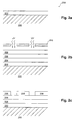
- FIGs. 2a-2e illustrate schematic cross-sectional views of a substrate 200 at different stages of an integrated circuit fabrication sequence incorporating a silicon carbide layer as a hardmask.
- the substrate 200 refers to any workpiece on which processing is performed, and a substrate structure 250 is used to generally denote the substrate together with other material layers formed on the substrate 200.
- the substrate 200 may correspond to a silicon wafer, or other material layer that has been formed on the silicon wafer.
- FIG 2a illustrates a cross-sectional view of a substrate structure 250, having a material layer 202 that has been conventionally formed thereon.
- the material layer 202 may be an oxide (e. g., silicon dioxide, fluorosilicate glass (FSG)).
- the substrate 200 may include a layer of silicon, silicides, metals, or other materials.
- FIG. 2a illustrates one embodiment in which the substrate 200 is silicon having a silicon dioxide layer formed thereon.
- FIG. 2b depicts a silicon carbide layer 204 formed on the substrate structure 250 of FIG. 2a.
- the silicon carbide layer 204 is formed on the substrate structure 250 according to the process parameters described above.
- the thickness of the silicon carbide layer is variable depending on the specific stage of processing. Typically, the silicon carbide layer is deposited to a thickness of about 50 ⁇ to about 1000 ⁇ .
- a layer of energy sensitive resist material 208 is formed on the silicon carbide layer 204.
- the layer of energy sensitive resist material 208 can be spin coated on the substrate to a thickness within a range of about 4,000 ⁇ to about 10,000 ⁇ .
- Most energy sensitive resist materials are sensitive to ultraviolet (UV) radiation having a wavelength less than about 450 nm (nanometers).
- Deep ultraviolet (DUV) resist materials are sensitive to UV radiation having wavelengths less than about 245 nm.
- an intermediate layer 206 is formed on the silicon carbide layer 204.
- the intermediate layer 206 functions as a mask for the silicon carbide layer 204.
- the intermediate layer 206 is conventionally formed on the silicon carbide layer 204.
- the intermediate layer 206 may be a silicon carbide cap layer, an oxide, nitride, silicon oxynitride, amorphous silicon, or other suitable material.
- An image of a pattern is introduced into the layer of energy sensitive resist material 208 by exposing such energy sensitive resist material 208 to UV radiation via mask 210.
- the image of the pattern introduced in the layer of energy sensitive resist material 208 is developed in an appropriate developer to define the pattern therethrough, as shown in FIG. 2c.
- the pattern defined in the energy sensitive resist material 208 is transferred through the silicon carbide layer 204.
- the pattern is transferred through the silicon carbide layer 204 using the energy sensitive resist material 208 as a mask.
- the pattern is transferred through the silicon carbide layer 204 using an appropriate chemical etchant.
- flourocarbon compounds such as trifluoromethane (CF 3 H) may be used to chemically etch the silicon carbide layer 204.
- the pattern defined in the energy sensitive resist material 208 is first transferred through the intermediate layer 206 using the energy sensitive resist material as a mask. Thereafter, the pattern is transferred through the silicon carbide layer 204 using the intermediate layer 206 as a mask. The pattern is transferred through both the intermediate layer 206 as well as the silicon carbide layer 204 using appropriate chemical etchants.
- FIG. 2e illustrates the completion of the integrated circuit fabrication sequence by the transfer of the pattern defined in the silicon carbide layer 204 through the silicon dioxide layer 202 using the silicon carbide layer 204 as a hardmask.
- the silicon carbide layer 204 can optionally be stripped from the substrate 200 by etching it in a suitable chemical etchant.
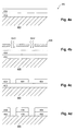
- FIGs. 3a-3g illustrate schematic cross-sectional views of a substrate 300 at different stages of a dual damascene structure fabrication sequence incorporating a silicon carbide barrier layer and a silicon carbide hard mask therein. Dual damascene structures are typically used to form multilayer metal interconnects on integrated circuits.
- substrate 300 may correspond to a silicon wafer, or other material layer that has been formed on the substrate 300.
- FIG. 3a illustrates a cross-sectional view of a substrate 300 having a metal layer 302 (e. g., copper (Cu), aluminum (Al), tungsten (W)) formed thereon.
- a metal layer 302 e. g., copper (Cu), aluminum (Al), tungsten (W)
- FIG. 3a illustrates one embodiment in which the substrate 300 is silicon having a copper (Cu) layer formed thereon.
- the copper layer 302 has a thickness of about 5,000 ⁇ to about 5 microns, depending on the size of the structure to be fabricated.
- a silicon carbide barrier layer 304 is formed on the copper layer 302.
- the silicon carbide barrier layer 304 is formed on the copper layer 302 according to the process parameters described above.
- the silicon carbide barrier layer 304 is compressive and has a dielectric constant less than about 5.5.
- the dielectric constant as well as the compressibility of the silicon carbide barrier layer is can be varied as a function of the gas composition (e. g., dopant concentration) during layer formation.
- the thickness of the silicon carbide barrier layer 304 is variable depending on the specific stage of processing. Typically, the silicon carbide barrier layer 304 has a thickness of about 200 ⁇ to about 1000 ⁇ .
- a first dielectric layer 305 is formed on the silicon carbide barrier layer 304, as illustrated in FIG. 3c.
- the first dielectric layer 305 may be an oxide (e. g., silicon dioxide, fluorosilicate glass (FSG)).
- the first dielectric layer 305 has a thickness of about 5,000 ⁇ to about 10,000 ⁇ .
- a silicon carbide hardmask layer 306 is formed on the first dielectric layer 305, patterned and etched to define vias therein.
- the silicon carbide hardmask layer 306 is formed on the first dielectric layer 305 according to the process parameters described above.
- the silicon carbide hardmask layer 306 is also compressive and has a dielectric constant less than about 5.5.
- the dielectric constant as well as the compressibility of the silicon carbide hardmask layer is can be varied as a function of the gas composition (e. g., dopant concentration) during layer formation.
- the thickness of the silicon carbide hardmask layer 306 is variable depending on the specific stage of processing. Typically, the silicon carbide hardmask layer 306 has a thickness of about 200 ⁇ to about 1000 ⁇ .
- the silicon carbide hardmask layer 306 is patterned and etched to define via openings 306 and to expose the first dielectric layer 305, in areas where the vias are to be formed.
- the silicon carbide hardmask layer 306 is patterned using conventional lithography as described above with reference to FIGs. 2b-2d.
- the silicon carbide layer is etched using a fluorocarbon compound such as trifluoromethane (CHF 3 ).
- a second dielectric layer 308 is deposited thereover, as illustrated in FIG. 3e.
- the second dielectric layer 308 may be an oxide (e. g., silicon dioxide, fluorosilicate glass).
- the second dielectric layer 308 has a thickness of about 5,000 ⁇ to about 10,000 ⁇ .
- the second dielectric layer 308 is then patterned to define interconnect lines 310, as illustrated in FIG. 3f, preferably using conventional lithography processes described above.
- the interconnects 310 formed in the second dielectric layer 308 are positioned over the via openings 306 in the silicon carbide hardmask layer 306. Thereafter, both the interconnects 310 and vias 306 are etched using reactive ion etching or other anisotropic etching techniques.
- the interconnects 310 and the vias 306 are filled with a conductive material 314 such as aluminum, copper, tungsten, or combinations thereof.
- a conductive material 314 such as aluminum, copper, tungsten, or combinations thereof.
- copper is used to fill the interconnects 310 and the vias 306, due to its low resistivity (resistivity about 1.7 ⁇ -cm).
- the conductive material 314 is deposited using chemical vapor deposition (CVD), physical vapor deposition (PVD), electroplating, or combinations thereof, to form the damascene structure.
- a barrier layer 316 such as tantalum (Ta), tantalum nitride (TaN), or other suitable barrier material is first deposited conformably on the sidewalls of the interconnects 310 and contacts/vias 306 to prevent metal migration into the surrounding dielectric layers 305, 308 as well as the silicon carbide barrier layer 304 and the silicon carbide hardmask layer 306.
- a barrier layer 316 such as tantalum (Ta), tantalum nitride (TaN), or other suitable barrier material is first deposited conformably on the sidewalls of the interconnects 310 and contacts/vias 306 to prevent metal migration into the surrounding dielectric layers 305, 308 as well as the silicon carbide barrier layer 304 and the silicon carbide hardmask layer 306.
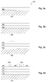
- FIGs. 4a-4e illustrate schematic cross-sectional views of a substrate 400 at different stages of an integrated circuit fabrication sequence incorporating a silicon carbide layer as an anti-reflective coating (ARC).
- the substrate 400 refers to any workpiece on which film processing is performed, and a substrate structure 450 is used to generally denote the substrate 400 together with other material layers formed on the substrate 400.
- substrate 400 may correspond to a silicon wafer, or other material layer, which has been formed on the substrate.
- FIG. 4a illustrates a cross-sectional view of a substrate structure 450 in which the substrate 400 is a silicon wafer having an oxide layer thereon.
- a silicon carbide layer 402 is formed on the substrate structure 450.
- the silicon carbide layer 402 is formed on the substrate structure 450 according to the process parameters described above.
- the silicon carbide layer has an absorption coefficient ( ⁇ ) that can be varied between about 0.1 to about 0.6 at wavelengths below about 250 nm (nanometers), making it suitable for use as an anti-reflective coating (ARC) at DUV wavelengths.
- the absorption coefficient of the silicon carbide layer is tunable, in that it can be varied in the desired range as a function of the gas composition.
- the thickness of the silicon carbide layer 402 is variable depending on the specific stage of processing. Typically, the silicon carbide layer has a thickness of about 200 ⁇ to about 2000 ⁇ .
- FIG. 4b depicts a layer of energy sensitive resist material 404 formed on the substrate structure 450 of FIG. 4a.
- the layer of energy sensitive resist material can be spin coated on the substrate structure 450 to a thickness within a range of about 2000 ⁇ to about 6000 ⁇ .
- the energy sensitive resist material is sensitive to DUV radiation having a wavelength less than 250 nm.
- An image of a pattern is introduced into the layer of energy sensitive resist material 404 by exposing such energy sensitive resist material 404 to DUV radiation via mask 406.
- the silicon carbide layer 402 suppresses any reflections off underlying material layers (e. g., oxides, metals) which can degrade the image of the pattern introduced in the layer of energy sensitive resist material 404.
- the image of the pattern introduced into the layer of energy sensitive resist material 404 is developed in an appropriate developer to define the pattern through such layer, as shown in FIG. 4c. Thereafter, referring to FIG. 4d, the pattern defined in the energy sensitive resist material 404 is transferred through the silicon carbide layer 402. The pattern is transferred through the silicon carbide layer 402 using the energy sensitive resist material 404 as a mask. The pattern is transferred through the silicon carbide layer 402 by etching it using an appropriate chemical etchant (e. g., CHF 3 ).
- an appropriate chemical etchant e. g., CHF 3
- the silicon carbide layer 402 is patterned, such pattern is typically transferred into the substrate 400, as shown in FIG. 4e.
- the pattern is transferred into the substrate 400 using the silicon carbide ARC layer 402 as a hardmask.
- the pattern is transferred into the substrate 400 by etching it using an appropriate chemical etchant.
- the silicon carbide layer 402 is optionally removed from the substrate structure 450 by etching it using an appropriate chemical etchant (e. g., CHF 3 ).
Landscapes
- Chemical & Material Sciences (AREA)
- Inorganic Chemistry (AREA)
- General Chemical & Material Sciences (AREA)
- Chemical Kinetics & Catalysis (AREA)
- Engineering & Computer Science (AREA)
- Materials Engineering (AREA)
- Mechanical Engineering (AREA)
- Metallurgy (AREA)
- Organic Chemistry (AREA)
- Internal Circuitry In Semiconductor Integrated Circuit Devices (AREA)
- Chemical Vapour Deposition (AREA)
- Formation Of Insulating Films (AREA)
Applications Claiming Priority (2)
| Application Number | Priority Date | Filing Date | Title |
|---|---|---|---|
| US09/627,667 US6764958B1 (en) | 2000-07-28 | 2000-07-28 | Method of depositing dielectric films |
| US627667 | 2000-07-28 |
Publications (2)
| Publication Number | Publication Date |
|---|---|
| EP1176226A1 true EP1176226A1 (de) | 2002-01-30 |
| EP1176226B1 EP1176226B1 (de) | 2009-05-06 |
Family
ID=24515594
Family Applications (1)
| Application Number | Title | Priority Date | Filing Date |
|---|---|---|---|
| EP01116054A Expired - Lifetime EP1176226B1 (de) | 2000-07-28 | 2001-07-02 | Verfahren zur Abscheidung einer Siliziumkarbidschicht zur Herstellung integrierter Schaltkreise |
Country Status (6)
| Country | Link |
|---|---|
| US (3) | US6764958B1 (de) |
| EP (1) | EP1176226B1 (de) |
| JP (1) | JP5027360B2 (de) |
| KR (1) | KR100801369B1 (de) |
| DE (1) | DE60138595D1 (de) |
| TW (1) | TW527670B (de) |
Cited By (21)
| Publication number | Priority date | Publication date | Assignee | Title |
|---|---|---|---|---|
| US6528423B1 (en) * | 2001-10-26 | 2003-03-04 | Lsi Logic Corporation | Process for forming composite of barrier layers of dielectric material to inhibit migration of copper from copper metal interconnect of integrated circuit structure into adjacent layer of low k dielectric material |
| WO2003052162A1 (en) * | 2001-12-14 | 2003-06-26 | Applied Materials, Inc. | A method of depositing dielectric materials in damascene applications |
| WO2003089681A3 (en) * | 2002-04-18 | 2004-01-22 | Applied Materials Inc | Mixed frequency high temperature nitride cvd process |
| US6759327B2 (en) | 2001-10-09 | 2004-07-06 | Applied Materials Inc. | Method of depositing low k barrier layers |
| US6806207B2 (en) | 1998-02-11 | 2004-10-19 | Applied Materials Inc. | Method of depositing low K films |
| EP1191123A3 (de) * | 2000-09-12 | 2004-11-17 | Applied Materials, Inc. | Zweifrequenzplasmaunterstützte chemische Dampfphasenabscheidung von Siliziumkarbidschichten |
| WO2004033752A3 (en) * | 2002-10-07 | 2004-12-09 | Applied Materials Inc | Two-layer film for next generation damascene barrier application with good oxidation resistance |
| US6838393B2 (en) | 2001-12-14 | 2005-01-04 | Applied Materials, Inc. | Method for producing semiconductor including forming a layer containing at least silicon carbide and forming a second layer containing at least silicon oxygen carbide |
| US6869896B2 (en) | 1998-02-11 | 2005-03-22 | Applied Materials, Inc. | Plasma processes for depositing low dielectric constant films |
| US6927178B2 (en) | 2002-07-11 | 2005-08-09 | Applied Materials, Inc. | Nitrogen-free dielectric anti-reflective coating and hardmask |
| US6930061B2 (en) | 1998-02-11 | 2005-08-16 | Applied Materials Inc. | Plasma processes for depositing low dielectric constant films |
| US6936309B2 (en) | 2002-04-02 | 2005-08-30 | Applied Materials, Inc. | Hardness improvement of silicon carboxy films |
| SG118174A1 (en) * | 2002-04-25 | 2006-01-27 | Taiwan Semiconductor Mfg | A method for forming a carbon doped oxide low-k insulating layer |
| US7030041B2 (en) | 2004-03-15 | 2006-04-18 | Applied Materials Inc. | Adhesion improvement for low k dielectrics |
| US7049249B2 (en) | 2003-01-13 | 2006-05-23 | Applied Materials | Method of improving stability in low k barrier layers |
| US7091137B2 (en) | 2001-12-14 | 2006-08-15 | Applied Materials | Bi-layer approach for a hermetic low dielectric constant layer for barrier applications |
| US7105460B2 (en) | 2002-07-11 | 2006-09-12 | Applied Materials | Nitrogen-free dielectric anti-reflective coating and hardmask |
| US7229911B2 (en) | 2004-04-19 | 2007-06-12 | Applied Materials, Inc. | Adhesion improvement for low k dielectrics to conductive materials |
| US7288205B2 (en) | 2004-07-09 | 2007-10-30 | Applied Materials, Inc. | Hermetic low dielectric constant layer for barrier applications |
| US7332445B2 (en) | 2004-09-28 | 2008-02-19 | Air Products And Chemicals, Inc. | Porous low dielectric constant compositions and methods for making and using same |
| RU2856760C1 (ru) * | 2025-09-25 | 2026-02-24 | федеральное государственное бюджетное образовательное учреждение высшего образования "Белгородский государственный технологический университет им. В.Г. Шухова" | Способ формирования пленки карбида кремния на подложке диоксида кремния |
Families Citing this family (206)
| Publication number | Priority date | Publication date | Assignee | Title |
|---|---|---|---|---|
| US6627532B1 (en) * | 1998-02-11 | 2003-09-30 | Applied Materials, Inc. | Method of decreasing the K value in SiOC layer deposited by chemical vapor deposition |
| US6821571B2 (en) * | 1999-06-18 | 2004-11-23 | Applied Materials Inc. | Plasma treatment to enhance adhesion and to minimize oxidation of carbon-containing layers |
| US6764958B1 (en) * | 2000-07-28 | 2004-07-20 | Applied Materials Inc. | Method of depositing dielectric films |
| US6537733B2 (en) * | 2001-02-23 | 2003-03-25 | Applied Materials, Inc. | Method of depositing low dielectric constant silicon carbide layers |
| US7432207B2 (en) * | 2001-08-31 | 2008-10-07 | Tokyo Electron Limited | Method for etching object to be processed |
| US6656837B2 (en) * | 2001-10-11 | 2003-12-02 | Applied Materials, Inc. | Method of eliminating photoresist poisoning in damascene applications |
| US7125812B2 (en) * | 2002-01-15 | 2006-10-24 | Tokyo Electron Limited | CVD method and device for forming silicon-containing insulation film |
| US6541397B1 (en) * | 2002-03-29 | 2003-04-01 | Applied Materials, Inc. | Removable amorphous carbon CMP stop |
| JP4066332B2 (ja) * | 2002-10-10 | 2008-03-26 | 日本エー・エス・エム株式会社 | シリコンカーバイド膜の製造方法 |
| US6991959B2 (en) * | 2002-10-10 | 2006-01-31 | Asm Japan K.K. | Method of manufacturing silicon carbide film |
| JP4119726B2 (ja) * | 2002-10-15 | 2008-07-16 | 東京エレクトロン株式会社 | プラズマ処理方法 |
| US20040124420A1 (en) * | 2002-12-31 | 2004-07-01 | Lin Simon S.H. | Etch stop layer |
| US7276441B1 (en) * | 2003-04-15 | 2007-10-02 | Lsi Logic Corporation | Dielectric barrier layer for increasing electromigration lifetimes in copper interconnect structures |
| KR100573484B1 (ko) | 2003-06-30 | 2006-04-24 | 에스티마이크로일렉트로닉스 엔.브이. | 반도체 소자 및 그 제조 방법 |
| US6849561B1 (en) * | 2003-08-18 | 2005-02-01 | Asm Japan K.K. | Method of forming low-k films |
| US7420275B1 (en) | 2003-09-24 | 2008-09-02 | Novellus Systems, Inc. | Boron-doped SIC copper diffusion barrier films |
| US6967405B1 (en) | 2003-09-24 | 2005-11-22 | Yongsik Yu | Film for copper diffusion barrier |
| US7261919B2 (en) * | 2003-11-18 | 2007-08-28 | Flx Micro, Inc. | Silicon carbide and other films and method of deposition |
| JP4715207B2 (ja) * | 2004-01-13 | 2011-07-06 | 東京エレクトロン株式会社 | 半導体装置の製造方法及び成膜システム |
| US20050230350A1 (en) | 2004-02-26 | 2005-10-20 | Applied Materials, Inc. | In-situ dry clean chamber for front end of line fabrication |
| US7282438B1 (en) | 2004-06-15 | 2007-10-16 | Novellus Systems, Inc. | Low-k SiC copper diffusion barrier films |
| US7253123B2 (en) * | 2005-01-10 | 2007-08-07 | Applied Materials, Inc. | Method for producing gate stack sidewall spacers |
| US7638859B2 (en) * | 2005-06-06 | 2009-12-29 | Taiwan Semiconductor Manufacturing Co., Ltd. | Interconnects with harmonized stress and methods for fabricating the same |
| US7977245B2 (en) * | 2006-03-22 | 2011-07-12 | Applied Materials, Inc. | Methods for etching a dielectric barrier layer with high selectivity |
| US7572482B2 (en) * | 2006-04-14 | 2009-08-11 | Bae Systems Information And Electronic Systems Integration Inc. | Photo-patterned carbon electronics |
| US20100178017A1 (en) * | 2006-10-06 | 2010-07-15 | Boris Kharas | Method for Improving Refractive Index Control in PECVD Deposited a-SiNy Films |
| US7915166B1 (en) | 2007-02-22 | 2011-03-29 | Novellus Systems, Inc. | Diffusion barrier and etch stop films |
| US8173537B1 (en) | 2007-03-29 | 2012-05-08 | Novellus Systems, Inc. | Methods for reducing UV and dielectric diffusion barrier interaction |
| US7678698B2 (en) | 2007-05-04 | 2010-03-16 | Freescale Semiconductor, Inc. | Method of forming a semiconductor device with multiple tensile stressor layers |
| US7964442B2 (en) * | 2007-10-09 | 2011-06-21 | Applied Materials, Inc. | Methods to obtain low k dielectric barrier with superior etch resistivity |
| US7700424B2 (en) * | 2008-02-27 | 2010-04-20 | Applied Materials, Inc. | Method of forming an embedded silicon carbon epitaxial layer |
| US8476742B2 (en) * | 2008-02-28 | 2013-07-02 | Hewlett-Packard Development Company, L.P. | Fluid ejection device comprising substrate contact via |
| US8124522B1 (en) | 2008-04-11 | 2012-02-28 | Novellus Systems, Inc. | Reducing UV and dielectric diffusion barrier interaction through the modulation of optical properties |
| US7759213B2 (en) * | 2008-08-11 | 2010-07-20 | International Business Machines Corporation | Pattern independent Si:C selective epitaxy |
| WO2010054204A2 (en) * | 2008-11-06 | 2010-05-14 | Uico, Inc. | Capacitive touch screen and strategic geometry isolation patterning method for making touch screens |
| US8247332B2 (en) * | 2009-12-04 | 2012-08-21 | Novellus Systems, Inc. | Hardmask materials |
| US9324576B2 (en) | 2010-05-27 | 2016-04-26 | Applied Materials, Inc. | Selective etch for silicon films |
| US10283321B2 (en) | 2011-01-18 | 2019-05-07 | Applied Materials, Inc. | Semiconductor processing system and methods using capacitively coupled plasma |
| US8771539B2 (en) | 2011-02-22 | 2014-07-08 | Applied Materials, Inc. | Remotely-excited fluorine and water vapor etch |
| US8999856B2 (en) | 2011-03-14 | 2015-04-07 | Applied Materials, Inc. | Methods for etch of sin films |
| US9064815B2 (en) | 2011-03-14 | 2015-06-23 | Applied Materials, Inc. | Methods for etch of metal and metal-oxide films |
| US8557682B2 (en) * | 2011-06-15 | 2013-10-15 | Applied Materials, Inc. | Multi-layer mask for substrate dicing by laser and plasma etch |
| US8771536B2 (en) | 2011-08-01 | 2014-07-08 | Applied Materials, Inc. | Dry-etch for silicon-and-carbon-containing films |
| US8679982B2 (en) | 2011-08-26 | 2014-03-25 | Applied Materials, Inc. | Selective suppression of dry-etch rate of materials containing both silicon and oxygen |
| US8679983B2 (en) | 2011-09-01 | 2014-03-25 | Applied Materials, Inc. | Selective suppression of dry-etch rate of materials containing both silicon and nitrogen |
| US8927390B2 (en) | 2011-09-26 | 2015-01-06 | Applied Materials, Inc. | Intrench profile |
| US8546204B2 (en) | 2011-10-03 | 2013-10-01 | International Business Machines Corporation | Method for growing conformal epi layers and structure thereof |
| US8808563B2 (en) | 2011-10-07 | 2014-08-19 | Applied Materials, Inc. | Selective etch of silicon by way of metastable hydrogen termination |
| WO2013070436A1 (en) | 2011-11-08 | 2013-05-16 | Applied Materials, Inc. | Methods of reducing substrate dislocation during gapfill processing |
| US10832904B2 (en) | 2012-06-12 | 2020-11-10 | Lam Research Corporation | Remote plasma based deposition of oxygen doped silicon carbide films |
| US10325773B2 (en) | 2012-06-12 | 2019-06-18 | Novellus Systems, Inc. | Conformal deposition of silicon carbide films |
| US9234276B2 (en) | 2013-05-31 | 2016-01-12 | Novellus Systems, Inc. | Method to obtain SiC class of films of desired composition and film properties |
| US10211310B2 (en) | 2012-06-12 | 2019-02-19 | Novellus Systems, Inc. | Remote plasma based deposition of SiOC class of films |
| US9267739B2 (en) | 2012-07-18 | 2016-02-23 | Applied Materials, Inc. | Pedestal with multi-zone temperature control and multiple purge capabilities |
| US9373517B2 (en) | 2012-08-02 | 2016-06-21 | Applied Materials, Inc. | Semiconductor processing with DC assisted RF power for improved control |
| US9034770B2 (en) | 2012-09-17 | 2015-05-19 | Applied Materials, Inc. | Differential silicon oxide etch |
| US9023734B2 (en) | 2012-09-18 | 2015-05-05 | Applied Materials, Inc. | Radical-component oxide etch |
| US9390937B2 (en) | 2012-09-20 | 2016-07-12 | Applied Materials, Inc. | Silicon-carbon-nitride selective etch |
| US9132436B2 (en) | 2012-09-21 | 2015-09-15 | Applied Materials, Inc. | Chemical control features in wafer process equipment |
| US8765574B2 (en) | 2012-11-09 | 2014-07-01 | Applied Materials, Inc. | Dry etch process |
| US8969212B2 (en) | 2012-11-20 | 2015-03-03 | Applied Materials, Inc. | Dry-etch selectivity |
| US9064816B2 (en) | 2012-11-30 | 2015-06-23 | Applied Materials, Inc. | Dry-etch for selective oxidation removal |
| US8980763B2 (en) | 2012-11-30 | 2015-03-17 | Applied Materials, Inc. | Dry-etch for selective tungsten removal |
| US9111877B2 (en) | 2012-12-18 | 2015-08-18 | Applied Materials, Inc. | Non-local plasma oxide etch |
| US9337068B2 (en) | 2012-12-18 | 2016-05-10 | Lam Research Corporation | Oxygen-containing ceramic hard masks and associated wet-cleans |
| US8921234B2 (en) | 2012-12-21 | 2014-12-30 | Applied Materials, Inc. | Selective titanium nitride etching |
| JP2014154666A (ja) * | 2013-02-07 | 2014-08-25 | Sumitomo Electric Ind Ltd | 炭化珪素半導体基板の製造方法および炭化珪素半導体装置の製造方法 |
| US10256079B2 (en) | 2013-02-08 | 2019-04-09 | Applied Materials, Inc. | Semiconductor processing systems having multiple plasma configurations |
| US9362130B2 (en) | 2013-03-01 | 2016-06-07 | Applied Materials, Inc. | Enhanced etching processes using remote plasma sources |
| US9040422B2 (en) | 2013-03-05 | 2015-05-26 | Applied Materials, Inc. | Selective titanium nitride removal |
| US8801952B1 (en) | 2013-03-07 | 2014-08-12 | Applied Materials, Inc. | Conformal oxide dry etch |
| US10170282B2 (en) | 2013-03-08 | 2019-01-01 | Applied Materials, Inc. | Insulated semiconductor faceplate designs |
| US20140271097A1 (en) | 2013-03-15 | 2014-09-18 | Applied Materials, Inc. | Processing systems and methods for halide scavenging |
| US8895449B1 (en) | 2013-05-16 | 2014-11-25 | Applied Materials, Inc. | Delicate dry clean |
| US9114438B2 (en) | 2013-05-21 | 2015-08-25 | Applied Materials, Inc. | Copper residue chamber clean |
| US10297442B2 (en) | 2013-05-31 | 2019-05-21 | Lam Research Corporation | Remote plasma based deposition of graded or multi-layered silicon carbide film |
| WO2014204028A1 (ko) * | 2013-06-18 | 2014-12-24 | 주식회사 원익아이피에스 | 박막 제조 방법 |
| US9493879B2 (en) | 2013-07-12 | 2016-11-15 | Applied Materials, Inc. | Selective sputtering for pattern transfer |
| US9773648B2 (en) | 2013-08-30 | 2017-09-26 | Applied Materials, Inc. | Dual discharge modes operation for remote plasma |
| US8956980B1 (en) | 2013-09-16 | 2015-02-17 | Applied Materials, Inc. | Selective etch of silicon nitride |
| US9371579B2 (en) | 2013-10-24 | 2016-06-21 | Lam Research Corporation | Ground state hydrogen radical sources for chemical vapor deposition of silicon-carbon-containing films |
| US8951429B1 (en) | 2013-10-29 | 2015-02-10 | Applied Materials, Inc. | Tungsten oxide processing |
| US9236265B2 (en) | 2013-11-04 | 2016-01-12 | Applied Materials, Inc. | Silicon germanium processing |
| US9576809B2 (en) | 2013-11-04 | 2017-02-21 | Applied Materials, Inc. | Etch suppression with germanium |
| US9520303B2 (en) | 2013-11-12 | 2016-12-13 | Applied Materials, Inc. | Aluminum selective etch |
| US9245762B2 (en) | 2013-12-02 | 2016-01-26 | Applied Materials, Inc. | Procedure for etch rate consistency |
| US9117855B2 (en) | 2013-12-04 | 2015-08-25 | Applied Materials, Inc. | Polarity control for remote plasma |
| US9287095B2 (en) | 2013-12-17 | 2016-03-15 | Applied Materials, Inc. | Semiconductor system assemblies and methods of operation |
| US9263278B2 (en) | 2013-12-17 | 2016-02-16 | Applied Materials, Inc. | Dopant etch selectivity control |
| US9190293B2 (en) | 2013-12-18 | 2015-11-17 | Applied Materials, Inc. | Even tungsten etch for high aspect ratio trenches |
| US9287134B2 (en) | 2014-01-17 | 2016-03-15 | Applied Materials, Inc. | Titanium oxide etch |
| US9293568B2 (en) | 2014-01-27 | 2016-03-22 | Applied Materials, Inc. | Method of fin patterning |
| US9396989B2 (en) | 2014-01-27 | 2016-07-19 | Applied Materials, Inc. | Air gaps between copper lines |
| US9385028B2 (en) | 2014-02-03 | 2016-07-05 | Applied Materials, Inc. | Air gap process |
| US9499898B2 (en) | 2014-03-03 | 2016-11-22 | Applied Materials, Inc. | Layered thin film heater and method of fabrication |
| US9299575B2 (en) | 2014-03-17 | 2016-03-29 | Applied Materials, Inc. | Gas-phase tungsten etch |
| US9299538B2 (en) | 2014-03-20 | 2016-03-29 | Applied Materials, Inc. | Radial waveguide systems and methods for post-match control of microwaves |
| US9299537B2 (en) | 2014-03-20 | 2016-03-29 | Applied Materials, Inc. | Radial waveguide systems and methods for post-match control of microwaves |
| US9136273B1 (en) | 2014-03-21 | 2015-09-15 | Applied Materials, Inc. | Flash gate air gap |
| US9903020B2 (en) | 2014-03-31 | 2018-02-27 | Applied Materials, Inc. | Generation of compact alumina passivation layers on aluminum plasma equipment components |
| US9269590B2 (en) | 2014-04-07 | 2016-02-23 | Applied Materials, Inc. | Spacer formation |
| US9309598B2 (en) | 2014-05-28 | 2016-04-12 | Applied Materials, Inc. | Oxide and metal removal |
| US9847289B2 (en) | 2014-05-30 | 2017-12-19 | Applied Materials, Inc. | Protective via cap for improved interconnect performance |
| US9378969B2 (en) | 2014-06-19 | 2016-06-28 | Applied Materials, Inc. | Low temperature gas-phase carbon removal |
| US9406523B2 (en) | 2014-06-19 | 2016-08-02 | Applied Materials, Inc. | Highly selective doped oxide removal method |
| US9425058B2 (en) | 2014-07-24 | 2016-08-23 | Applied Materials, Inc. | Simplified litho-etch-litho-etch process |
| US9496167B2 (en) | 2014-07-31 | 2016-11-15 | Applied Materials, Inc. | Integrated bit-line airgap formation and gate stack post clean |
| US9159606B1 (en) | 2014-07-31 | 2015-10-13 | Applied Materials, Inc. | Metal air gap |
| US9378978B2 (en) | 2014-07-31 | 2016-06-28 | Applied Materials, Inc. | Integrated oxide recess and floating gate fin trimming |
| US9165786B1 (en) | 2014-08-05 | 2015-10-20 | Applied Materials, Inc. | Integrated oxide and nitride recess for better channel contact in 3D architectures |
| US9659753B2 (en) | 2014-08-07 | 2017-05-23 | Applied Materials, Inc. | Grooved insulator to reduce leakage current |
| US9553102B2 (en) | 2014-08-19 | 2017-01-24 | Applied Materials, Inc. | Tungsten separation |
| US9355856B2 (en) | 2014-09-12 | 2016-05-31 | Applied Materials, Inc. | V trench dry etch |
| US9355862B2 (en) | 2014-09-24 | 2016-05-31 | Applied Materials, Inc. | Fluorine-based hardmask removal |
| US9368364B2 (en) | 2014-09-24 | 2016-06-14 | Applied Materials, Inc. | Silicon etch process with tunable selectivity to SiO2 and other materials |
| US9613822B2 (en) | 2014-09-25 | 2017-04-04 | Applied Materials, Inc. | Oxide etch selectivity enhancement |
| US9966240B2 (en) | 2014-10-14 | 2018-05-08 | Applied Materials, Inc. | Systems and methods for internal surface conditioning assessment in plasma processing equipment |
| US9355922B2 (en) | 2014-10-14 | 2016-05-31 | Applied Materials, Inc. | Systems and methods for internal surface conditioning in plasma processing equipment |
| US11637002B2 (en) | 2014-11-26 | 2023-04-25 | Applied Materials, Inc. | Methods and systems to enhance process uniformity |
| US9299583B1 (en) | 2014-12-05 | 2016-03-29 | Applied Materials, Inc. | Aluminum oxide selective etch |
| US10573496B2 (en) | 2014-12-09 | 2020-02-25 | Applied Materials, Inc. | Direct outlet toroidal plasma source |
| US10224210B2 (en) | 2014-12-09 | 2019-03-05 | Applied Materials, Inc. | Plasma processing system with direct outlet toroidal plasma source |
| US9502258B2 (en) | 2014-12-23 | 2016-11-22 | Applied Materials, Inc. | Anisotropic gap etch |
| US9343272B1 (en) | 2015-01-08 | 2016-05-17 | Applied Materials, Inc. | Self-aligned process |
| US11257693B2 (en) | 2015-01-09 | 2022-02-22 | Applied Materials, Inc. | Methods and systems to improve pedestal temperature control |
| US9373522B1 (en) | 2015-01-22 | 2016-06-21 | Applied Mateials, Inc. | Titanium nitride removal |
| US9449846B2 (en) | 2015-01-28 | 2016-09-20 | Applied Materials, Inc. | Vertical gate separation |
| US20160225652A1 (en) | 2015-02-03 | 2016-08-04 | Applied Materials, Inc. | Low temperature chuck for plasma processing systems |
| US9728437B2 (en) | 2015-02-03 | 2017-08-08 | Applied Materials, Inc. | High temperature chuck for plasma processing systems |
| US9881805B2 (en) | 2015-03-02 | 2018-01-30 | Applied Materials, Inc. | Silicon selective removal |
| US20160314964A1 (en) | 2015-04-21 | 2016-10-27 | Lam Research Corporation | Gap fill using carbon-based films |
| US9691645B2 (en) | 2015-08-06 | 2017-06-27 | Applied Materials, Inc. | Bolted wafer chuck thermal management systems and methods for wafer processing systems |
| US9741593B2 (en) | 2015-08-06 | 2017-08-22 | Applied Materials, Inc. | Thermal management systems and methods for wafer processing systems |
| US9349605B1 (en) | 2015-08-07 | 2016-05-24 | Applied Materials, Inc. | Oxide etch selectivity systems and methods |
| US10504700B2 (en) | 2015-08-27 | 2019-12-10 | Applied Materials, Inc. | Plasma etching systems and methods with secondary plasma injection |
| US10522371B2 (en) | 2016-05-19 | 2019-12-31 | Applied Materials, Inc. | Systems and methods for improved semiconductor etching and component protection |
| US10504754B2 (en) | 2016-05-19 | 2019-12-10 | Applied Materials, Inc. | Systems and methods for improved semiconductor etching and component protection |
| US9865484B1 (en) | 2016-06-29 | 2018-01-09 | Applied Materials, Inc. | Selective etch using material modification and RF pulsing |
| US10858727B2 (en) | 2016-08-19 | 2020-12-08 | Applied Materials, Inc. | High density, low stress amorphous carbon film, and process and equipment for its deposition |
| US10062575B2 (en) | 2016-09-09 | 2018-08-28 | Applied Materials, Inc. | Poly directional etch by oxidation |
| US10629473B2 (en) | 2016-09-09 | 2020-04-21 | Applied Materials, Inc. | Footing removal for nitride spacer |
| US9721789B1 (en) | 2016-10-04 | 2017-08-01 | Applied Materials, Inc. | Saving ion-damaged spacers |
| US10062585B2 (en) | 2016-10-04 | 2018-08-28 | Applied Materials, Inc. | Oxygen compatible plasma source |
| US9934942B1 (en) | 2016-10-04 | 2018-04-03 | Applied Materials, Inc. | Chamber with flow-through source |
| US10546729B2 (en) | 2016-10-04 | 2020-01-28 | Applied Materials, Inc. | Dual-channel showerhead with improved profile |
| US10062579B2 (en) | 2016-10-07 | 2018-08-28 | Applied Materials, Inc. | Selective SiN lateral recess |
| US9947549B1 (en) | 2016-10-10 | 2018-04-17 | Applied Materials, Inc. | Cobalt-containing material removal |
| US10163696B2 (en) | 2016-11-11 | 2018-12-25 | Applied Materials, Inc. | Selective cobalt removal for bottom up gapfill |
| US9768034B1 (en) | 2016-11-11 | 2017-09-19 | Applied Materials, Inc. | Removal methods for high aspect ratio structures |
| US10026621B2 (en) | 2016-11-14 | 2018-07-17 | Applied Materials, Inc. | SiN spacer profile patterning |
| US10242908B2 (en) | 2016-11-14 | 2019-03-26 | Applied Materials, Inc. | Airgap formation with damage-free copper |
| US10002787B2 (en) | 2016-11-23 | 2018-06-19 | Lam Research Corporation | Staircase encapsulation in 3D NAND fabrication |
| US9837270B1 (en) | 2016-12-16 | 2017-12-05 | Lam Research Corporation | Densification of silicon carbide film using remote plasma treatment |
| US10566206B2 (en) | 2016-12-27 | 2020-02-18 | Applied Materials, Inc. | Systems and methods for anisotropic material breakthrough |
| US10403507B2 (en) | 2017-02-03 | 2019-09-03 | Applied Materials, Inc. | Shaped etch profile with oxidation |
| US10431429B2 (en) | 2017-02-03 | 2019-10-01 | Applied Materials, Inc. | Systems and methods for radial and azimuthal control of plasma uniformity |
| US10043684B1 (en) | 2017-02-06 | 2018-08-07 | Applied Materials, Inc. | Self-limiting atomic thermal etching systems and methods |
| US10319739B2 (en) | 2017-02-08 | 2019-06-11 | Applied Materials, Inc. | Accommodating imperfectly aligned memory holes |
| US10943834B2 (en) | 2017-03-13 | 2021-03-09 | Applied Materials, Inc. | Replacement contact process |
| EP3382068B1 (de) * | 2017-03-29 | 2022-05-18 | SiCrystal GmbH | Siliciumcarbidsubstrat und verfahren zur züchtung von sic-einkristall-ingots |
| US10319649B2 (en) | 2017-04-11 | 2019-06-11 | Applied Materials, Inc. | Optical emission spectroscopy (OES) for remote plasma monitoring |
| US11276559B2 (en) | 2017-05-17 | 2022-03-15 | Applied Materials, Inc. | Semiconductor processing chamber for multiple precursor flow |
| JP7176860B6 (ja) | 2017-05-17 | 2022-12-16 | アプライド マテリアルズ インコーポレイテッド | 前駆体の流れを改善する半導体処理チャンバ |
| US11276590B2 (en) | 2017-05-17 | 2022-03-15 | Applied Materials, Inc. | Multi-zone semiconductor substrate supports |
| US10049891B1 (en) | 2017-05-31 | 2018-08-14 | Applied Materials, Inc. | Selective in situ cobalt residue removal |
| US10497579B2 (en) | 2017-05-31 | 2019-12-03 | Applied Materials, Inc. | Water-free etching methods |
| US10920320B2 (en) | 2017-06-16 | 2021-02-16 | Applied Materials, Inc. | Plasma health determination in semiconductor substrate processing reactors |
| US10541246B2 (en) | 2017-06-26 | 2020-01-21 | Applied Materials, Inc. | 3D flash memory cells which discourage cross-cell electrical tunneling |
| US10727080B2 (en) | 2017-07-07 | 2020-07-28 | Applied Materials, Inc. | Tantalum-containing material removal |
| US10541184B2 (en) | 2017-07-11 | 2020-01-21 | Applied Materials, Inc. | Optical emission spectroscopic techniques for monitoring etching |
| US10354889B2 (en) | 2017-07-17 | 2019-07-16 | Applied Materials, Inc. | Non-halogen etching of silicon-containing materials |
| US10170336B1 (en) | 2017-08-04 | 2019-01-01 | Applied Materials, Inc. | Methods for anisotropic control of selective silicon removal |
| US10043674B1 (en) | 2017-08-04 | 2018-08-07 | Applied Materials, Inc. | Germanium etching systems and methods |
| US10297458B2 (en) | 2017-08-07 | 2019-05-21 | Applied Materials, Inc. | Process window widening using coated parts in plasma etch processes |
| US10128086B1 (en) | 2017-10-24 | 2018-11-13 | Applied Materials, Inc. | Silicon pretreatment for nitride removal |
| US10283324B1 (en) | 2017-10-24 | 2019-05-07 | Applied Materials, Inc. | Oxygen treatment for nitride etching |
| US10256112B1 (en) | 2017-12-08 | 2019-04-09 | Applied Materials, Inc. | Selective tungsten removal |
| US10903054B2 (en) | 2017-12-19 | 2021-01-26 | Applied Materials, Inc. | Multi-zone gas distribution systems and methods |
| US11328909B2 (en) | 2017-12-22 | 2022-05-10 | Applied Materials, Inc. | Chamber conditioning and removal processes |
| US10854426B2 (en) | 2018-01-08 | 2020-12-01 | Applied Materials, Inc. | Metal recess for semiconductor structures |
| US10964512B2 (en) | 2018-02-15 | 2021-03-30 | Applied Materials, Inc. | Semiconductor processing chamber multistage mixing apparatus and methods |
| US10679870B2 (en) | 2018-02-15 | 2020-06-09 | Applied Materials, Inc. | Semiconductor processing chamber multistage mixing apparatus |
| TWI766433B (zh) | 2018-02-28 | 2022-06-01 | 美商應用材料股份有限公司 | 形成氣隙的系統及方法 |
| US10593560B2 (en) | 2018-03-01 | 2020-03-17 | Applied Materials, Inc. | Magnetic induction plasma source for semiconductor processes and equipment |
| US10319600B1 (en) | 2018-03-12 | 2019-06-11 | Applied Materials, Inc. | Thermal silicon etch |
| US10497573B2 (en) | 2018-03-13 | 2019-12-03 | Applied Materials, Inc. | Selective atomic layer etching of semiconductor materials |
| US10573527B2 (en) | 2018-04-06 | 2020-02-25 | Applied Materials, Inc. | Gas-phase selective etching systems and methods |
| US10490406B2 (en) | 2018-04-10 | 2019-11-26 | Appled Materials, Inc. | Systems and methods for material breakthrough |
| US10699879B2 (en) | 2018-04-17 | 2020-06-30 | Applied Materials, Inc. | Two piece electrode assembly with gap for plasma control |
| US10886137B2 (en) | 2018-04-30 | 2021-01-05 | Applied Materials, Inc. | Selective nitride removal |
| US10755941B2 (en) | 2018-07-06 | 2020-08-25 | Applied Materials, Inc. | Self-limiting selective etching systems and methods |
| US10872778B2 (en) | 2018-07-06 | 2020-12-22 | Applied Materials, Inc. | Systems and methods utilizing solid-phase etchants |
| US10672642B2 (en) | 2018-07-24 | 2020-06-02 | Applied Materials, Inc. | Systems and methods for pedestal configuration |
| US10892198B2 (en) | 2018-09-14 | 2021-01-12 | Applied Materials, Inc. | Systems and methods for improved performance in semiconductor processing |
| US11049755B2 (en) | 2018-09-14 | 2021-06-29 | Applied Materials, Inc. | Semiconductor substrate supports with embedded RF shield |
| US11062887B2 (en) | 2018-09-17 | 2021-07-13 | Applied Materials, Inc. | High temperature RF heater pedestals |
| US11417534B2 (en) | 2018-09-21 | 2022-08-16 | Applied Materials, Inc. | Selective material removal |
| JP2022501833A (ja) * | 2018-10-05 | 2022-01-06 | ラム リサーチ コーポレーションLam Research Corporation | プラズマ処理チャンバ |
| US11682560B2 (en) | 2018-10-11 | 2023-06-20 | Applied Materials, Inc. | Systems and methods for hafnium-containing film removal |
| US11121002B2 (en) | 2018-10-24 | 2021-09-14 | Applied Materials, Inc. | Systems and methods for etching metals and metal derivatives |
| US11437242B2 (en) | 2018-11-27 | 2022-09-06 | Applied Materials, Inc. | Selective removal of silicon-containing materials |
| US11721527B2 (en) | 2019-01-07 | 2023-08-08 | Applied Materials, Inc. | Processing chamber mixing systems |
| US10920319B2 (en) | 2019-01-11 | 2021-02-16 | Applied Materials, Inc. | Ceramic showerheads with conductive electrodes |
| JP2020136387A (ja) * | 2019-02-15 | 2020-08-31 | 東京エレクトロン株式会社 | 成膜方法、成膜処理用の処理容器のクリーニング方法及び成膜装置 |
| US11515147B2 (en) * | 2019-12-09 | 2022-11-29 | Micron Technology, Inc. | Material deposition systems, and related methods |
| US11577217B2 (en) * | 2019-12-12 | 2023-02-14 | Praxair Technology, Inc. | Dopant fluid storage and dispensing systems utilizing high performance, structurally modified particulate carbon adsorbents |
Citations (4)
| Publication number | Priority date | Publication date | Assignee | Title |
|---|---|---|---|---|
| EP0926715A2 (de) * | 1997-12-23 | 1999-06-30 | Texas Instruments Incorporated | Chemisch-mechanishes Polieren für die Planarisierung isolierender Dielektrika |
| EP0926724A2 (de) * | 1997-12-12 | 1999-06-30 | Texas Instruments Incorporated | Strukturierung von porösem Silizium mittels einer Silizumkarbid-Maske |
| US5953627A (en) * | 1997-11-06 | 1999-09-14 | International Business Machines Corporation | Process for manufacture of integrated circuit device |
| WO2000019498A1 (en) | 1998-10-01 | 2000-04-06 | Applied Materials, Inc. | In situ deposition of low k si carbide barrier layer, etch stop, and anti-reflective coating for damascene applications |
Family Cites Families (57)
| Publication number | Priority date | Publication date | Assignee | Title |
|---|---|---|---|---|
| DE2364989C3 (de) | 1973-12-28 | 1979-10-18 | Consortium Fuer Elektrochemische Industrie Gmbh, 8000 Muenchen | Verfahren zur Herstellung von Schichten aus Siliciumcarbid auf einem Siliciumsubstrat |
| US4262631A (en) | 1979-10-01 | 1981-04-21 | Kubacki Ronald M | Thin film deposition apparatus using an RF glow discharge |
| JPS59128281A (ja) | 1982-12-29 | 1984-07-24 | 信越化学工業株式会社 | 炭化けい素被覆物の製造方法 |
| JPH07111957B2 (ja) | 1984-03-28 | 1995-11-29 | 圭弘 浜川 | 半導体の製法 |
| US4759947A (en) | 1984-10-08 | 1988-07-26 | Canon Kabushiki Kaisha | Method for forming deposition film using Si compound and active species from carbon and halogen compound |
| JPS61257475A (ja) | 1985-05-08 | 1986-11-14 | Tdk Corp | 保護膜 |
| US5300951A (en) | 1985-11-28 | 1994-04-05 | Kabushiki Kaisha Toshiba | Member coated with ceramic material and method of manufacturing the same |
| US4822697A (en) | 1986-12-03 | 1989-04-18 | Dow Corning Corporation | Platinum and rhodium catalysis of low temperature formation multilayer ceramics |
| JP2546696B2 (ja) | 1987-12-17 | 1996-10-23 | 富士通株式会社 | シリコン炭化層構造 |
| US5082695A (en) | 1988-03-08 | 1992-01-21 | 501 Fujitsu Limited | Method of fabricating an x-ray exposure mask |
| US4885220A (en) | 1988-05-25 | 1989-12-05 | Xerox Corporation | Amorphous silicon carbide electroreceptors |
| US4894352A (en) | 1988-10-26 | 1990-01-16 | Texas Instruments Inc. | Deposition of silicon-containing films using organosilicon compounds and nitrogen trifluoride |
| US5238866A (en) | 1991-09-11 | 1993-08-24 | GmbH & Co. Ingenieurburo Berlin Biotronik Mess- und Therapiegerate | Plasma enhanced chemical vapor deposition process for producing an amorphous semiconductive surface coating |
| US5472829A (en) | 1991-12-30 | 1995-12-05 | Sony Corporation | Method of forming a resist pattern by using an anti-reflective layer |
| US5597566A (en) | 1992-05-06 | 1997-01-28 | Ford Motor Company | Vibration damping universal joint |
| US5465680A (en) | 1993-07-01 | 1995-11-14 | Dow Corning Corporation | Method of forming crystalline silicon carbide coatings |
| JP2641385B2 (ja) | 1993-09-24 | 1997-08-13 | アプライド マテリアルズ インコーポレイテッド | 膜形成方法 |
| US5818071A (en) | 1995-02-02 | 1998-10-06 | Dow Corning Corporation | Silicon carbide metal diffusion barrier layer |
| TW362118B (en) | 1995-10-30 | 1999-06-21 | Dow Corning | Method for depositing amorphous SiNC coatings |
| US5759746A (en) | 1996-05-24 | 1998-06-02 | Kabushiki Kaisha Toshiba | Fabrication process using a thin resist |
| US5989998A (en) | 1996-08-29 | 1999-11-23 | Matsushita Electric Industrial Co., Ltd. | Method of forming interlayer insulating film |
| US5711987A (en) | 1996-10-04 | 1998-01-27 | Dow Corning Corporation | Electronic coatings |
| JPH10223758A (ja) | 1996-12-06 | 1998-08-21 | Sony Corp | 半導体装置 |
| US5926740A (en) * | 1997-10-27 | 1999-07-20 | Micron Technology, Inc. | Graded anti-reflective coating for IC lithography |
| US6051321A (en) | 1997-10-24 | 2000-04-18 | Quester Technology, Inc. | Low dielectric constant materials and method |
| US6041734A (en) | 1997-12-01 | 2000-03-28 | Applied Materials, Inc. | Use of an asymmetric waveform to control ion bombardment during substrate processing |
| US6555476B1 (en) | 1997-12-23 | 2003-04-29 | Texas Instruments Incorporated | Silicon carbide as a stop layer in chemical mechanical polishing for isolation dielectric |
| US6140226A (en) | 1998-01-16 | 2000-10-31 | International Business Machines Corporation | Dual damascene processing for semiconductor chip interconnects |
| US6054379A (en) | 1998-02-11 | 2000-04-25 | Applied Materials, Inc. | Method of depositing a low k dielectric with organo silane |
| US6627532B1 (en) | 1998-02-11 | 2003-09-30 | Applied Materials, Inc. | Method of decreasing the K value in SiOC layer deposited by chemical vapor deposition |
| US6287990B1 (en) | 1998-02-11 | 2001-09-11 | Applied Materials, Inc. | CVD plasma assisted low dielectric constant films |
| WO1999046128A1 (en) * | 1998-03-10 | 1999-09-16 | Diamonex, Incorporated | Highly wear-resistant thermal print heads with silicon-doped diamond-like carbon protective coatings |
| US6068884A (en) | 1998-04-28 | 2000-05-30 | Silcon Valley Group Thermal Systems, Llc | Method of making low κ dielectric inorganic/organic hybrid films |
| US6159871A (en) | 1998-05-29 | 2000-12-12 | Dow Corning Corporation | Method for producing hydrogenated silicon oxycarbide films having low dielectric constant |
| US6060132A (en) | 1998-06-15 | 2000-05-09 | Siemens Aktiengesellschaft | High density plasma CVD process for making dielectric anti-reflective coatings |
| US6147009A (en) | 1998-06-29 | 2000-11-14 | International Business Machines Corporation | Hydrogenated oxidized silicon carbon material |
| US6316167B1 (en) | 2000-01-10 | 2001-11-13 | International Business Machines Corporation | Tunabale vapor deposited materials as antireflective coatings, hardmasks and as combined antireflective coating/hardmasks and methods of fabrication thereof and application thereof |
| US6462371B1 (en) | 1998-11-24 | 2002-10-08 | Micron Technology Inc. | Films doped with carbon for use in integrated circuit technology |
| US6364954B2 (en) | 1998-12-14 | 2002-04-02 | Applied Materials, Inc. | High temperature chemical vapor deposition chamber |
| US6312793B1 (en) | 1999-05-26 | 2001-11-06 | International Business Machines Corporation | Multiphase low dielectric constant material |
| US6436824B1 (en) * | 1999-07-02 | 2002-08-20 | Chartered Semiconductor Manufacturing Ltd. | Low dielectric constant materials for copper damascene |
| US6593653B2 (en) | 1999-09-30 | 2003-07-15 | Novellus Systems, Inc. | Low leakage current silicon carbonitride prepared using methane, ammonia and silane for copper diffusion barrier, etchstop and passivation applications |
| US6417092B1 (en) | 2000-04-05 | 2002-07-09 | Novellus Systems, Inc. | Low dielectric constant etch stop films |
| US6429129B1 (en) | 2000-06-16 | 2002-08-06 | Chartered Semiconductor Manufacturing Ltd. | Method of using silicon rich carbide as a barrier material for fluorinated materials |
| JP2002009069A (ja) | 2000-06-22 | 2002-01-11 | Canon Sales Co Inc | 成膜方法 |
| US6410437B1 (en) * | 2000-06-30 | 2002-06-25 | Lam Research Corporation | Method for etching dual damascene structures in organosilicate glass |
| JP3934343B2 (ja) | 2000-07-12 | 2007-06-20 | キヤノンマーケティングジャパン株式会社 | 半導体装置及びその製造方法 |
| US6794311B2 (en) | 2000-07-14 | 2004-09-21 | Applied Materials Inc. | Method and apparatus for treating low k dielectric layers to reduce diffusion |
| US6764958B1 (en) * | 2000-07-28 | 2004-07-20 | Applied Materials Inc. | Method of depositing dielectric films |
| US6465366B1 (en) | 2000-09-12 | 2002-10-15 | Applied Materials, Inc. | Dual frequency plasma enhanced chemical vapor deposition of silicon carbide layers |
| US6340628B1 (en) | 2000-12-12 | 2002-01-22 | Novellus Systems, Inc. | Method to deposit SiOCH films with dielectric constant below 3.0 |
| US6537733B2 (en) | 2001-02-23 | 2003-03-25 | Applied Materials, Inc. | Method of depositing low dielectric constant silicon carbide layers |
| US6506692B2 (en) | 2001-05-30 | 2003-01-14 | Intel Corporation | Method of making a semiconductor device using a silicon carbide hard mask |
| US6534397B1 (en) | 2001-07-13 | 2003-03-18 | Advanced Micro Devices, Inc. | Pre-treatment of low-k dielectric for prevention of photoresist poisoning |
| US20030045125A1 (en) | 2001-09-05 | 2003-03-06 | Taiwan Semiconductor Manufacturing Co., Ltd. | Nitrogen containing plasma annealing method for forming a nitrogenated silicon carbide layer |
| US6528423B1 (en) | 2001-10-26 | 2003-03-04 | Lsi Logic Corporation | Process for forming composite of barrier layers of dielectric material to inhibit migration of copper from copper metal interconnect of integrated circuit structure into adjacent layer of low k dielectric material |
| US6849562B2 (en) * | 2002-03-04 | 2005-02-01 | Applied Materials, Inc. | Method of depositing a low k dielectric barrier film for copper damascene application |
-
2000
- 2000-07-28 US US09/627,667 patent/US6764958B1/en not_active Expired - Fee Related
-
2001
- 2001-05-11 TW TW090111381A patent/TW527670B/zh not_active IP Right Cessation
- 2001-06-22 KR KR1020010035740A patent/KR100801369B1/ko not_active Expired - Fee Related
- 2001-07-02 EP EP01116054A patent/EP1176226B1/de not_active Expired - Lifetime
- 2001-07-02 DE DE60138595T patent/DE60138595D1/de not_active Expired - Fee Related
- 2001-07-30 JP JP2001230269A patent/JP5027360B2/ja not_active Expired - Fee Related
-
2004
- 2004-07-20 US US10/894,872 patent/US7001850B2/en not_active Expired - Fee Related
-
2006
- 2006-02-21 US US11/358,793 patent/US7117064B2/en not_active Expired - Fee Related
Patent Citations (5)
| Publication number | Priority date | Publication date | Assignee | Title |
|---|---|---|---|---|
| US5953627A (en) * | 1997-11-06 | 1999-09-14 | International Business Machines Corporation | Process for manufacture of integrated circuit device |
| EP0926724A2 (de) * | 1997-12-12 | 1999-06-30 | Texas Instruments Incorporated | Strukturierung von porösem Silizium mittels einer Silizumkarbid-Maske |
| EP0926715A2 (de) * | 1997-12-23 | 1999-06-30 | Texas Instruments Incorporated | Chemisch-mechanishes Polieren für die Planarisierung isolierender Dielektrika |
| WO2000019498A1 (en) | 1998-10-01 | 2000-04-06 | Applied Materials, Inc. | In situ deposition of low k si carbide barrier layer, etch stop, and anti-reflective coating for damascene applications |
| WO2000019508A1 (en) * | 1998-10-01 | 2000-04-06 | Applied Materials, Inc. | Silicon carbide deposition method and use as a barrier layer and passivation layer |
Non-Patent Citations (2)
| Title |
|---|
| CHAUDHURI PARTHA; DAS ULLWAL KUMAR: "Argon assisted Plasma Chemical Vapour Deposition of Amorphous Silicon Carbide Films", JPN. J. APPL. PHYS., vol. 36, 1997, pages L1426 - L1429 |
| J. SAFRANKOVA ET AL.: "Vacuum", vol. 51, 1998, ELSEVIER SCIENCE LTD, article ""Characterization of nitrogen-doped amorphous silicon carbide thin films", pages: 165 - 167 |
Cited By (30)
| Publication number | Priority date | Publication date | Assignee | Title |
|---|---|---|---|---|
| US6869896B2 (en) | 1998-02-11 | 2005-03-22 | Applied Materials, Inc. | Plasma processes for depositing low dielectric constant films |
| US6930061B2 (en) | 1998-02-11 | 2005-08-16 | Applied Materials Inc. | Plasma processes for depositing low dielectric constant films |
| US6806207B2 (en) | 1998-02-11 | 2004-10-19 | Applied Materials Inc. | Method of depositing low K films |
| US7560377B2 (en) | 1998-02-11 | 2009-07-14 | Applied Materials, Inc. | Plasma processes for depositing low dielectric constant films |
| EP1191123A3 (de) * | 2000-09-12 | 2004-11-17 | Applied Materials, Inc. | Zweifrequenzplasmaunterstützte chemische Dampfphasenabscheidung von Siliziumkarbidschichten |
| US7319068B2 (en) | 2001-10-09 | 2008-01-15 | Applied Materials, Inc. | Method of depositing low k barrier layers |
| US6759327B2 (en) | 2001-10-09 | 2004-07-06 | Applied Materials Inc. | Method of depositing low k barrier layers |
| US7125813B2 (en) | 2001-10-09 | 2006-10-24 | Applied Materials, Inc. | Method of depositing low K barrier layers |
| US6528423B1 (en) * | 2001-10-26 | 2003-03-04 | Lsi Logic Corporation | Process for forming composite of barrier layers of dielectric material to inhibit migration of copper from copper metal interconnect of integrated circuit structure into adjacent layer of low k dielectric material |
| US6890850B2 (en) | 2001-12-14 | 2005-05-10 | Applied Materials, Inc. | Method of depositing dielectric materials in damascene applications |
| US7157384B2 (en) | 2001-12-14 | 2007-01-02 | Applied Materials, Inc. | Low dielectric (low k) barrier films with oxygen doping by plasma-enhanced chemical vapor deposition (PECVD) |
| US6838393B2 (en) | 2001-12-14 | 2005-01-04 | Applied Materials, Inc. | Method for producing semiconductor including forming a layer containing at least silicon carbide and forming a second layer containing at least silicon oxygen carbide |
| US7091137B2 (en) | 2001-12-14 | 2006-08-15 | Applied Materials | Bi-layer approach for a hermetic low dielectric constant layer for barrier applications |
| US7151053B2 (en) | 2001-12-14 | 2006-12-19 | Applied Materials, Inc. | Method of depositing dielectric materials including oxygen-doped silicon carbide in damascene applications |
| US7745328B2 (en) | 2001-12-14 | 2010-06-29 | Applied Materials, Inc. | Low dielectric (low k) barrier films with oxygen doping by plasma-enhanced chemical vapor deposition (PECVD) |
| WO2003052162A1 (en) * | 2001-12-14 | 2003-06-26 | Applied Materials, Inc. | A method of depositing dielectric materials in damascene applications |
| US6936309B2 (en) | 2002-04-02 | 2005-08-30 | Applied Materials, Inc. | Hardness improvement of silicon carboxy films |
| WO2003089681A3 (en) * | 2002-04-18 | 2004-01-22 | Applied Materials Inc | Mixed frequency high temperature nitride cvd process |
| SG118174A1 (en) * | 2002-04-25 | 2006-01-27 | Taiwan Semiconductor Mfg | A method for forming a carbon doped oxide low-k insulating layer |
| US7105460B2 (en) | 2002-07-11 | 2006-09-12 | Applied Materials | Nitrogen-free dielectric anti-reflective coating and hardmask |
| US6927178B2 (en) | 2002-07-11 | 2005-08-09 | Applied Materials, Inc. | Nitrogen-free dielectric anti-reflective coating and hardmask |
| US7749563B2 (en) | 2002-10-07 | 2010-07-06 | Applied Materials, Inc. | Two-layer film for next generation damascene barrier application with good oxidation resistance |
| WO2004033752A3 (en) * | 2002-10-07 | 2004-12-09 | Applied Materials Inc | Two-layer film for next generation damascene barrier application with good oxidation resistance |
| US7049249B2 (en) | 2003-01-13 | 2006-05-23 | Applied Materials | Method of improving stability in low k barrier layers |
| US7030041B2 (en) | 2004-03-15 | 2006-04-18 | Applied Materials Inc. | Adhesion improvement for low k dielectrics |
| US7459404B2 (en) | 2004-03-15 | 2008-12-02 | Applied Materials, Inc. | Adhesion improvement for low k dielectrics |
| US7229911B2 (en) | 2004-04-19 | 2007-06-12 | Applied Materials, Inc. | Adhesion improvement for low k dielectrics to conductive materials |
| US7288205B2 (en) | 2004-07-09 | 2007-10-30 | Applied Materials, Inc. | Hermetic low dielectric constant layer for barrier applications |
| US7332445B2 (en) | 2004-09-28 | 2008-02-19 | Air Products And Chemicals, Inc. | Porous low dielectric constant compositions and methods for making and using same |
| RU2856760C1 (ru) * | 2025-09-25 | 2026-02-24 | федеральное государственное бюджетное образовательное учреждение высшего образования "Белгородский государственный технологический университет им. В.Г. Шухова" | Способ формирования пленки карбида кремния на подложке диоксида кремния |
Also Published As
| Publication number | Publication date |
|---|---|
| KR20020010073A (ko) | 2002-02-02 |
| JP2002190522A (ja) | 2002-07-05 |
| US20060141805A1 (en) | 2006-06-29 |
| US7001850B2 (en) | 2006-02-21 |
| EP1176226B1 (de) | 2009-05-06 |
| US7117064B2 (en) | 2006-10-03 |
| US20050020048A1 (en) | 2005-01-27 |
| DE60138595D1 (de) | 2009-06-18 |
| US6764958B1 (en) | 2004-07-20 |
| KR100801369B1 (ko) | 2008-02-05 |
| JP5027360B2 (ja) | 2012-09-19 |
| TW527670B (en) | 2003-04-11 |
Similar Documents
| Publication | Publication Date | Title |
|---|---|---|
| US6764958B1 (en) | Method of depositing dielectric films | |
| US6537733B2 (en) | Method of depositing low dielectric constant silicon carbide layers | |
| US6589888B2 (en) | Dual frequency plasma enhanced chemical vapor deposition of silicon carbide layers | |
| US6500773B1 (en) | Method of depositing organosilicate layers | |
| US6777171B2 (en) | Fluorine-containing layers for damascene structures | |
| US6632735B2 (en) | Method of depositing low dielectric constant carbon doped silicon oxide | |
| US6531398B1 (en) | Method of depositing organosillicate layers | |
| US7244672B2 (en) | Selective etching of organosilicate films over silicon oxide stop etch layers | |
| US6573196B1 (en) | Method of depositing organosilicate layers | |
| US6750141B2 (en) | Silicon carbide cap layers for low dielectric constant silicon oxide layers | |
| EP1186685A2 (de) | Herstellungsverfahren von Siliziumkarbid-Filmen | |
| US6521546B1 (en) | Method of making a fluoro-organosilicate layer | |
| US20020142104A1 (en) | Plasma treatment of organosilicate layers |
Legal Events
| Date | Code | Title | Description |
|---|---|---|---|
| PUAI | Public reference made under article 153(3) epc to a published international application that has entered the european phase |
Free format text: ORIGINAL CODE: 0009012 |
|
| AK | Designated contracting states |
Kind code of ref document: A1 Designated state(s): DE GB Kind code of ref document: A1 Designated state(s): AT BE CH CY DE DK ES FI FR GB GR IE IT LI LU MC NL PT SE TR |
|
| AX | Request for extension of the european patent |
Free format text: AL;LT;LV;MK;RO;SI |
|
| RIN1 | Information on inventor provided before grant (corrected) |
Inventor name: YIEH, ELLIE Inventor name: CAMPANA-SCHMITT, FRANCIMAR Inventor name: XU, PING Inventor name: SUGIARTO, DIAN Inventor name: XIA, LI-QUN Inventor name: NEMANI, SRINIVAS D. Inventor name: LEE, JIA |
|
| 17P | Request for examination filed |
Effective date: 20020730 |
|
| AKX | Designation fees paid |
Free format text: DE GB |
|
| 17Q | First examination report despatched |
Effective date: 20080704 |
|
| GRAP | Despatch of communication of intention to grant a patent |
Free format text: ORIGINAL CODE: EPIDOSNIGR1 |
|
| GRAS | Grant fee paid |
Free format text: ORIGINAL CODE: EPIDOSNIGR3 |
|
| GRAA | (expected) grant |
Free format text: ORIGINAL CODE: 0009210 |
|
| AK | Designated contracting states |
Kind code of ref document: B1 Designated state(s): DE GB |
|
| REG | Reference to a national code |
Ref country code: GB Ref legal event code: FG4D |
|
| REF | Corresponds to: |
Ref document number: 60138595 Country of ref document: DE Date of ref document: 20090618 Kind code of ref document: P |
|
| PLBE | No opposition filed within time limit |
Free format text: ORIGINAL CODE: 0009261 |
|
| STAA | Information on the status of an ep patent application or granted ep patent |
Free format text: STATUS: NO OPPOSITION FILED WITHIN TIME LIMIT |
|
| 26N | No opposition filed |
Effective date: 20100209 |
|
| GBPC | Gb: european patent ceased through non-payment of renewal fee |
Effective date: 20090806 |
|
| PG25 | Lapsed in a contracting state [announced via postgrant information from national office to epo] |
Ref country code: DE Free format text: LAPSE BECAUSE OF NON-PAYMENT OF DUE FEES Effective date: 20100202 |
|
| PG25 | Lapsed in a contracting state [announced via postgrant information from national office to epo] |
Ref country code: GB Free format text: LAPSE BECAUSE OF NON-PAYMENT OF DUE FEES Effective date: 20090806 |