EP0926733B1 - Ensemble formant une carte comprenant un dispositif de puissance dans un boitier en plastique avec un dissipateur thermique externe soudé au dissipateur thermique interne - Google Patents
Ensemble formant une carte comprenant un dispositif de puissance dans un boitier en plastique avec un dissipateur thermique externe soudé au dissipateur thermique interne Download PDFInfo
- Publication number
- EP0926733B1 EP0926733B1 EP97830677A EP97830677A EP0926733B1 EP 0926733 B1 EP0926733 B1 EP 0926733B1 EP 97830677 A EP97830677 A EP 97830677A EP 97830677 A EP97830677 A EP 97830677A EP 0926733 B1 EP0926733 B1 EP 0926733B1
- Authority
- EP
- European Patent Office
- Prior art keywords
- heat sink
- metal
- external
- printed circuit
- metal slug
- Prior art date
- Legal status (The legal status is an assumption and is not a legal conclusion. Google has not performed a legal analysis and makes no representation as to the accuracy of the status listed.)
- Expired - Lifetime
Links
Images



Classifications
-
- H—ELECTRICITY
- H10—SEMICONDUCTOR DEVICES; ELECTRIC SOLID-STATE DEVICES NOT OTHERWISE PROVIDED FOR
- H10W—GENERIC PACKAGES, INTERCONNECTIONS, CONNECTORS OR OTHER CONSTRUCTIONAL DETAILS OF DEVICES COVERED BY CLASS H10
- H10W40/00—Arrangements for thermal protection or thermal control
- H10W40/20—Arrangements for cooling
- H10W40/22—Arrangements for cooling characterised by their shape, e.g. having conical or cylindrical projections
-
- H—ELECTRICITY
- H05—ELECTRIC TECHNIQUES NOT OTHERWISE PROVIDED FOR
- H05K—PRINTED CIRCUITS; CASINGS OR CONSTRUCTIONAL DETAILS OF ELECTRIC APPARATUS; MANUFACTURE OF ASSEMBLAGES OF ELECTRICAL COMPONENTS
- H05K3/00—Apparatus or processes for manufacturing printed circuits
- H05K3/30—Assembling printed circuits with electric components, e.g. with resistors
- H05K3/32—Assembling printed circuits with electric components, e.g. with resistors electrically connecting electric components or wires to printed circuits
- H05K3/34—Assembling printed circuits with electric components, e.g. with resistors electrically connecting electric components or wires to printed circuits by soldering
- H05K3/341—Surface mounted components
-
- H—ELECTRICITY
- H05—ELECTRIC TECHNIQUES NOT OTHERWISE PROVIDED FOR
- H05K—PRINTED CIRCUITS; CASINGS OR CONSTRUCTIONAL DETAILS OF ELECTRIC APPARATUS; MANUFACTURE OF ASSEMBLAGES OF ELECTRICAL COMPONENTS
- H05K1/00—Printed circuits
- H05K1/02—Details
- H05K1/0201—Thermal arrangements, e.g. for cooling, heating or preventing overheating
- H05K1/0203—Cooling of mounted components
-
- H—ELECTRICITY
- H05—ELECTRIC TECHNIQUES NOT OTHERWISE PROVIDED FOR
- H05K—PRINTED CIRCUITS; CASINGS OR CONSTRUCTIONAL DETAILS OF ELECTRIC APPARATUS; MANUFACTURE OF ASSEMBLAGES OF ELECTRICAL COMPONENTS
- H05K2201/00—Indexing scheme relating to printed circuits covered by H05K1/00
- H05K2201/06—Thermal details
- H05K2201/066—Heatsink mounted on the surface of the printed circuit board [PCB]
-
- H—ELECTRICITY
- H05—ELECTRIC TECHNIQUES NOT OTHERWISE PROVIDED FOR
- H05K—PRINTED CIRCUITS; CASINGS OR CONSTRUCTIONAL DETAILS OF ELECTRIC APPARATUS; MANUFACTURE OF ASSEMBLAGES OF ELECTRICAL COMPONENTS
- H05K2201/00—Indexing scheme relating to printed circuits covered by H05K1/00
- H05K2201/10—Details of components or other objects attached to or integrated in a printed circuit board
- H05K2201/10613—Details of electrical connections of non-printed components, e.g. special leads
- H05K2201/10621—Components characterised by their electrical contacts
- H05K2201/10689—Leaded Integrated Circuit [IC] package, e.g. dual-in-line [DIL]
-
- H—ELECTRICITY
- H05—ELECTRIC TECHNIQUES NOT OTHERWISE PROVIDED FOR
- H05K—PRINTED CIRCUITS; CASINGS OR CONSTRUCTIONAL DETAILS OF ELECTRIC APPARATUS; MANUFACTURE OF ASSEMBLAGES OF ELECTRICAL COMPONENTS
- H05K2201/00—Indexing scheme relating to printed circuits covered by H05K1/00
- H05K2201/10—Details of components or other objects attached to or integrated in a printed circuit board
- H05K2201/10613—Details of electrical connections of non-printed components, e.g. special leads
- H05K2201/10954—Other details of electrical connections
- H05K2201/10969—Metallic case or integral heatsink of component electrically connected to a pad on PCB
-
- Y—GENERAL TAGGING OF NEW TECHNOLOGICAL DEVELOPMENTS; GENERAL TAGGING OF CROSS-SECTIONAL TECHNOLOGIES SPANNING OVER SEVERAL SECTIONS OF THE IPC; TECHNICAL SUBJECTS COVERED BY FORMER USPC CROSS-REFERENCE ART COLLECTIONS [XRACs] AND DIGESTS
- Y02—TECHNOLOGIES OR APPLICATIONS FOR MITIGATION OR ADAPTATION AGAINST CLIMATE CHANGE
- Y02P—CLIMATE CHANGE MITIGATION TECHNOLOGIES IN THE PRODUCTION OR PROCESSING OF GOODS
- Y02P70/00—Climate change mitigation technologies in the production process for final industrial or consumer products
- Y02P70/50—Manufacturing or production processes characterised by the final manufactured product
Definitions
- the present invention relates to techniques of dissipation of the heat generated inside integrated devices encapsulated in a plastic package for assembly, on the surface of a printed circuit board.
- the problem of dissipating the heat generated within the integrated circuit and to maintain the internal temperature of a package, typically of plastic material, below a maximum tolerable value, is particularly relevant when assembling power devices packages on the surface of a printed circuit board.
- a first approach is that of patterning copper pad on the printed circuit onto which the internal heat sink of the power device package is soldered. In this manner the heat generated inside the device may be effectively transferred to the external world through the copper pad exploiting a spreading effect over the printed circuit board.
- holes are realized within the copper pad. These holes have their inner wall covered with a film of copper and constitute as many conductive vias for transferring heat across the thickness of the board to the other side of it where another dedicated copper pad may be patterned, on which an external metal sink may be placed or alternately contacted by the metal chassis of the apparatus.
- the metal coated holes do not cross the whole thickness of the board but reach a ground metallization layer sandwiched therein, typically in the form of a copper film, perfectly suitable to disperse the heat throughout the board.
- Another known solution consists of printed circuit boards specially realized on a relatively thick metal substrate of a thermally conductive material such as aluminum.
- the system of the invention applies to any power device wherein the metal slug (internal metal heat sink) of the power device package has at least a portion projecting out of the surface of at least one side of the package commonly a molded body of encapsulating resin.
- An external metal heat sink having a shape suited to couple with the particular package of the power device surface-mounted on a printed circuit board, has at least a surface bearing on the package in a manner as to leave a gap between the protruding part of the metal heat sink incorporated in the package and a surface spacingly opposed to it of the external metal heat sink.
- the gap being readily encroached and filled by the molten eutectic tin/lead alloy during a normal soldering step of the devices and components installed on a printed circuit board.
- the internal metal slug has a portion that extends from the plane of the bottom encapsulating resin body of the power device package.
- the external metal heat sink has a base that is substantially shaped as a flat frame, whose dimensions are coordinated with the package dimensions so that the protruding part of the metal slug of the package remains contained in the aperture of the bottom frame portion of the external heat sink, on the sides of which bear the recessed perimetral part of the bottom of the molded body of encapsulating resin of the package that surrounds the protruding part of the metal slug.
- an effective thermally conducting bridge is realized that favors heat transfer from the metal slug to the external heat sink.
- the internal heat sink protrudes from two opposed sides of the molded body of resin of the power device package, at the bottom of the latter, that rests on the patterned layer of soldering paste defined on the component assembly side of the board.
- the external metal heat sink is shaped so to be placed over the power device.
- the external metal heat sink has two legs that extend toward the surface of the printed circuit board along the above mentioned sides of the package, and which bear on the printed layer of soldering paste, thus defining a gap between each laterally extending part of the metal slug and the inner face side of the relative vertical leg of the external metal sink opposed to it.
- Such a small vertical gap is at least partially encroached by the liquefied eutectic alloy during the soldering phase thus soldering permanently each of the two laterally protruding parts of the internal metal slug to the opposed leg of the external heat sink placed over the device.
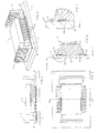
- FIG. 1 to 7 refer to a first embodiment of the invention.
- the same parts and features are identified with the same numbers in the different figures.
- an internal metal heat sink (or simply slug) 3 commonly of a highly conducting metal such as copper or nickel coated copper, onto which is bonded the silicon chip or dice of the integrated circuit, is only partially buried in the molded body of the encapsulating resin and protrudes for a certain height from the bottom face of the device 1, commonly configured for surface-assembly on a printed circuit board 7.
- the external metal heat sink 2 has a substantially flat base shaped as a rectangular frame 5, the dimensions of the central aperture 6 of the frame being coordinated with the dimensions of the protruding part of the internal metal slug 3 of the power package 1, so to accommodate such a protruding part in the aperture 6.
- the device 1 is positioned on the printed circuit board 7 after having positioned thereon the external metal heat sink 2 so that the recessed perimetral part of the bottom side surrounding the protruding metal slug 3 may rest on the four sides of the flat frame 5, whose thickness may be approximately identical to the height of the protruding part of the metal slug 3 emerging out of the bottom side of the molded resin body 4. They may both rest on the patterned layer of soldering paste 8 preventively screen printed on the surface of the board 7.
- the molten eutectic alloy 8 tends to fill at least partially, the gap 10, finally soldering the internal metal slug 3 to the flat frame 5 of the external metal heat sink.
- the metal heat sink 3 protrudes laterally out of two opposed sides of the encapsulating resin body 4 of the device 1.
- the system of the invention permits to realize assemblies that include an external metal heat sink that can be mounted on power devices surface mounted on the printed circuit board, notwithstanding the fact that the power devices be of the so-called "slug-down" type.
Landscapes
- Engineering & Computer Science (AREA)
- Manufacturing & Machinery (AREA)
- Microelectronics & Electronic Packaging (AREA)
- Cooling Or The Like Of Semiconductors Or Solid State Devices (AREA)
Claims (3)
- Montage d'un radiateur externe (2) soudé à une pièce métallique (3) incorporée au fond d'un corps moulé (4) de résine d'encapsulation du boítier d'un dispositif de puissance intégré monté en surface sur la surface d'une carte de circuit imprimé (7), caractérisé en ce que :la pièce métallique (3) comporte au moins une partie faisant saillie à partir d'une surface externe d'au moins une face du corps (4) ;le radiateur métallique externe (2) est placé sur la surface de la carte de circuit imprimé (7) et comporte une première et une seconde partie, de sorte qu'au moins la première partie (5, 9a, 9b) repose sur la surface de la carte de circuit imprimé (7) et a au moins une surface en butée avec une surface du corps (4) de sorte qu'un intervalle de séparation (10) est défini entre au moins une surface de la partie en saillie de la pièce métallique (3) et une surface de la première partie (5, 9a, 9b) qui lui est opposée, l'intervalle de séparation étant rempli d'un alliage de soudure (8).
- Montage selon la revendication 1, caractérisé en outre en ce que la pièce métallique (3) fait saillie à partir du côté inférieur du corps de résine (4) sur une partie de la surface du fond du corps de résine et la première partie du radiateur métallique externe (2) comprend un châssis de base sensiblement plat (5) d'une dimension telle que la partie en saillie de la pièce métallique (3) du boítier s'adapte dans une ouverture (6) du châssis de base plat (5) sur lequel bute une partie périphérique évidée du fond du corps de résine (4) entourant la partie en saillie (3), en laissant ledit intervalle (10) entre une surface périphérique externe de la partie en saillie de la pièce métallique (3) et une partie périphérique interne de l'ouverture (6), l'intervalle étant rempli de l'alliage de soudure (8).
- Montage selon la revendication 1, caractérisé en outre en ce que la pièce métallique (3) fait saillie à partir de deux faces latérales opposées du corps de résine (4) et le radiateur métallique externe (2) a une forme convenable pour que la seconde partie du radiateur externe (2) soit placée sur le dispositif et en ce que la première partie du radiateur externe comprend deux pattes (9a, 9b) s'étendant vers la surface de la carte de circuit imprimé (7) le long des deux faces latérales du corps de résine (4) et définissant ledit intervalle de séparation (10) entre chaque partie en saillie de la pièce métallique (3) et la surface interne de la patte respective (9a, 9b) qui lui est opposée, l'intervalle étant rempli de l'alliage de soudure (8).
Priority Applications (4)
| Application Number | Priority Date | Filing Date | Title |
|---|---|---|---|
| EP97830677A EP0926733B1 (fr) | 1997-12-16 | 1997-12-16 | Ensemble formant une carte comprenant un dispositif de puissance dans un boitier en plastique avec un dissipateur thermique externe soudé au dissipateur thermique interne |
| DE69728153T DE69728153D1 (de) | 1997-12-16 | 1997-12-16 | Leiterplattenanordnung bestehend aus einem in einem Kunststoffgehäuse verpackten Leistungshalbleiterbauelement, dessen interne Wärmesenke mit einer externen Wärmesenke gelötet ist |
| US09/211,426 US6195256B1 (en) | 1997-12-16 | 1998-12-15 | Card assembly of power device in plastic package with external heat sink soldered to the internal heat sink |
| JP10356463A JPH11312769A (ja) | 1997-12-16 | 1998-12-15 | デバイス放熱用のヒートシンクアセンブリ |
Applications Claiming Priority (1)
| Application Number | Priority Date | Filing Date | Title |
|---|---|---|---|
| EP97830677A EP0926733B1 (fr) | 1997-12-16 | 1997-12-16 | Ensemble formant une carte comprenant un dispositif de puissance dans un boitier en plastique avec un dissipateur thermique externe soudé au dissipateur thermique interne |
Publications (2)
| Publication Number | Publication Date |
|---|---|
| EP0926733A1 EP0926733A1 (fr) | 1999-06-30 |
| EP0926733B1 true EP0926733B1 (fr) | 2004-03-17 |
Family
ID=8230898
Family Applications (1)
| Application Number | Title | Priority Date | Filing Date |
|---|---|---|---|
| EP97830677A Expired - Lifetime EP0926733B1 (fr) | 1997-12-16 | 1997-12-16 | Ensemble formant une carte comprenant un dispositif de puissance dans un boitier en plastique avec un dissipateur thermique externe soudé au dissipateur thermique interne |
Country Status (4)
| Country | Link |
|---|---|
| US (1) | US6195256B1 (fr) |
| EP (1) | EP0926733B1 (fr) |
| JP (1) | JPH11312769A (fr) |
| DE (1) | DE69728153D1 (fr) |
Families Citing this family (20)
| Publication number | Priority date | Publication date | Assignee | Title |
|---|---|---|---|---|
| EP1113495B1 (fr) * | 1999-12-30 | 2007-03-21 | Texas Instruments Incorporated | Transistor de puissance monté en surface avec dissipateur thermique |
| AT409954B (de) * | 2000-04-06 | 2002-12-27 | Thyssenkrupp Presta Ag | Mehrteiliges mantelrohr für eine lenkwelle |
| EP1268253B1 (fr) | 2000-04-06 | 2006-08-30 | ThyssenKrupp Presta Aktiengesellschaft | Logement de support pour un arbre de direction |
| US6483706B2 (en) * | 2000-12-22 | 2002-11-19 | Vlt Corporation | Heat dissipation for electronic components |
| US20030168730A1 (en) * | 2002-03-08 | 2003-09-11 | Howard Davidson | Carbon foam heat exchanger for integrated circuit |
| JP2007527105A (ja) * | 2003-06-06 | 2007-09-20 | ハネウエル・インターナシヨナル・インコーポレーテツド | 熱連結システムとその製造方法 |
| US6987317B2 (en) | 2003-09-30 | 2006-01-17 | Intel Corporation | Power delivery using an integrated heat spreader |
| US7345364B2 (en) * | 2004-02-04 | 2008-03-18 | Agere Systems Inc. | Structure and method for improved heat conduction for semiconductor devices |
| US7233497B2 (en) * | 2004-10-06 | 2007-06-19 | Hewlett-Packard Development Company, L.P. | Surface mount heat sink |
| DE102006009812B4 (de) * | 2006-03-01 | 2008-09-04 | Beru Ag | Montageanordnung für mehrere Leistungshalbleiter und Schaltung mit einer solchen Montageanordnung |
| US20090323288A1 (en) * | 2008-06-30 | 2009-12-31 | Bernard Marc R | Heat sink slack storage and adaptive operation |
| WO2012151347A1 (fr) * | 2011-05-03 | 2012-11-08 | Vishay Dale Electronics, Inc. | Dispositif de dispersion de chaleur pour composants électriques |
| CN102299127B (zh) * | 2011-07-13 | 2013-12-11 | 台达电子企业管理(上海)有限公司 | 用于封装元件的双向散热器及其组装方法 |
| US9484280B2 (en) * | 2014-01-11 | 2016-11-01 | Infineon Technologies Austria Ag | Semiconductor device and method of manufacturing a semiconductor device |
| WO2017027315A1 (fr) | 2015-08-07 | 2017-02-16 | Vishay Dale Electronics, Llc | Corps moulé et dispositif électrique comportant un corps moulé destiné à des applications haute tension |
| US10123460B2 (en) * | 2015-11-13 | 2018-11-06 | Covidien LLP | System and method for thermal management of electronic devices |
| DE102019206523A1 (de) * | 2019-05-07 | 2020-11-12 | Zf Friedrichshafen Ag | Leistungsmodul mit gehäusten Leistungshalbleitern zur steuerbaren elektrischen Leistungsversorgung eines Verbrauchers |
| CN110729546A (zh) * | 2019-10-18 | 2020-01-24 | 大连大学 | 一种5g天线散热器 |
| US11908771B2 (en) | 2021-11-12 | 2024-02-20 | Infineon Technologies Ag | Power semiconductor device with dual heat dissipation structures |
| CN116489943A (zh) * | 2023-03-30 | 2023-07-25 | 华为数字能源技术有限公司 | 散热器及功率变换器件 |
Family Cites Families (10)
| Publication number | Priority date | Publication date | Assignee | Title |
|---|---|---|---|---|
| JPS5471572A (en) * | 1977-11-18 | 1979-06-08 | Fujitsu Ltd | Semiconductor device |
| JPS57117263A (en) * | 1981-01-12 | 1982-07-21 | Mitsubishi Electric Corp | Cooler for dual-in-line package type integrated circuit element |
| JPS5947750A (ja) * | 1982-09-10 | 1984-03-17 | Hitachi Ltd | 面取付型半導体装置 |
| JPS6292347A (ja) * | 1985-10-17 | 1987-04-27 | Mitsubishi Electric Corp | 半導体装置用放熱フイン |
| FR2625038B1 (fr) * | 1987-12-22 | 1990-08-17 | Cit Alcatel | Procede et dispositif de refroidissement d'un boitier de circuit integre |
| US4914551A (en) * | 1988-07-13 | 1990-04-03 | International Business Machines Corporation | Electronic package with heat spreader member |
| US5216283A (en) * | 1990-05-03 | 1993-06-01 | Motorola, Inc. | Semiconductor device having an insertable heat sink and method for mounting the same |
| JP2882116B2 (ja) * | 1991-09-13 | 1999-04-12 | 日本電気株式会社 | ヒートシンク付パッケージ |
| JP3086340B2 (ja) * | 1992-08-04 | 2000-09-11 | ローム株式会社 | ヒートシンク付き電子部品のプリント基板への半田実装方法 |
| US5272599A (en) * | 1993-03-19 | 1993-12-21 | Compaq Computer Corporation | Microprocessor heat dissipation apparatus for a printed circuit board |
-
1997
- 1997-12-16 EP EP97830677A patent/EP0926733B1/fr not_active Expired - Lifetime
- 1997-12-16 DE DE69728153T patent/DE69728153D1/de not_active Expired - Lifetime
-
1998
- 1998-12-15 JP JP10356463A patent/JPH11312769A/ja active Pending
- 1998-12-15 US US09/211,426 patent/US6195256B1/en not_active Expired - Lifetime
Also Published As
| Publication number | Publication date |
|---|---|
| JPH11312769A (ja) | 1999-11-09 |
| DE69728153D1 (de) | 2004-04-22 |
| US6195256B1 (en) | 2001-02-27 |
| EP0926733A1 (fr) | 1999-06-30 |
Similar Documents
| Publication | Publication Date | Title |
|---|---|---|
| EP0926733A1 (fr) | Ensemble formant une carte comprenant un dispositif de puissance dans un boitier en plastique avec un dissipateur thermique externe soudé au dissipateur thermique interne | |
| JP3414342B2 (ja) | 集積回路チップの実装構造および実装方法 | |
| US5708566A (en) | Solder bonded electronic module | |
| EP0338249B1 (fr) | Empaquetage électronique | |
| JP3056960B2 (ja) | 半導体装置及びbgaパッケージ | |
| US5895973A (en) | Electronic component assembly for maintaining component alignment during soldering | |
| JP3196762B2 (ja) | 半導体チップ冷却構造 | |
| US7006353B2 (en) | Apparatus and method for attaching a heat sink to an integrated circuit module | |
| KR19990062847A (ko) | 전자회로를 패키징하는 방법 및 그 조립체 | |
| US5841198A (en) | Ball grid array package employing solid core solder balls | |
| US6034437A (en) | Semiconductor device having a matrix of bonding pads | |
| US6166435A (en) | Flip-chip ball grid array package with a heat slug | |
| JPH08250835A (ja) | 金属バンプを有するlsiパッケージの実装方法 | |
| US6441480B1 (en) | Microelectronic circuit package | |
| JP2772828B2 (ja) | ダイボンディング方法 | |
| JP2817712B2 (ja) | 半導体装置及びその実装方法 | |
| JPH09283675A (ja) | 放熱フィン取付構造 | |
| US5679979A (en) | Surface mount package with heat transfer feature | |
| JP3959839B2 (ja) | 半導体装置の製造方法 | |
| KR0156513B1 (ko) | 반도체패키지 | |
| JP2000252406A (ja) | 電子回路装置 | |
| JP2734684B2 (ja) | 半導体素子パッケージ | |
| JPH0621269Y2 (ja) | セラミック回路基板 | |
| KR200228982Y1 (ko) | 파워 모듈 패키지용 케이스의 구조 | |
| KR0120612Y1 (ko) | 인쇄회로기판 내장형 반도체 패키지 |
Legal Events
| Date | Code | Title | Description |
|---|---|---|---|
| PUAI | Public reference made under article 153(3) epc to a published international application that has entered the european phase |
Free format text: ORIGINAL CODE: 0009012 |
|
| AK | Designated contracting states |
Kind code of ref document: A1 Designated state(s): DE FR GB IT |
|
| AX | Request for extension of the european patent |
Free format text: AL;LT;LV;MK;RO;SI |
|
| 17P | Request for examination filed |
Effective date: 19990922 |
|
| AKX | Designation fees paid |
Free format text: AT BE CH DE LI |
|
| RBV | Designated contracting states (corrected) |
Designated state(s): DE FR GB IT |
|
| 17Q | First examination report despatched |
Effective date: 20010613 |
|
| GRAP | Despatch of communication of intention to grant a patent |
Free format text: ORIGINAL CODE: EPIDOSNIGR1 |
|
| GRAS | Grant fee paid |
Free format text: ORIGINAL CODE: EPIDOSNIGR3 |
|
| GRAA | (expected) grant |
Free format text: ORIGINAL CODE: 0009210 |
|
| AK | Designated contracting states |
Kind code of ref document: B1 Designated state(s): DE FR GB IT |
|
| PG25 | Lapsed in a contracting state [announced via postgrant information from national office to epo] |
Ref country code: FR Free format text: LAPSE BECAUSE OF FAILURE TO SUBMIT A TRANSLATION OF THE DESCRIPTION OR TO PAY THE FEE WITHIN THE PRESCRIBED TIME-LIMIT Effective date: 20040317 |
|
| REG | Reference to a national code |
Ref country code: GB Ref legal event code: FG4D |
|
| REF | Corresponds to: |
Ref document number: 69728153 Country of ref document: DE Date of ref document: 20040422 Kind code of ref document: P |
|
| PG25 | Lapsed in a contracting state [announced via postgrant information from national office to epo] |
Ref country code: DE Free format text: LAPSE BECAUSE OF FAILURE TO SUBMIT A TRANSLATION OF THE DESCRIPTION OR TO PAY THE FEE WITHIN THE PRESCRIBED TIME-LIMIT Effective date: 20040618 |
|
| PG25 | Lapsed in a contracting state [announced via postgrant information from national office to epo] |
Ref country code: GB Free format text: LAPSE BECAUSE OF NON-PAYMENT OF DUE FEES Effective date: 20041216 |
|
| PLBE | No opposition filed within time limit |
Free format text: ORIGINAL CODE: 0009261 |
|
| STAA | Information on the status of an ep patent application or granted ep patent |
Free format text: STATUS: NO OPPOSITION FILED WITHIN TIME LIMIT |
|
| EN | Fr: translation not filed | ||
| 26N | No opposition filed |
Effective date: 20041220 |
|
| GBPC | Gb: european patent ceased through non-payment of renewal fee |
Effective date: 20041216 |
|
| PGFP | Annual fee paid to national office [announced via postgrant information from national office to epo] |
Ref country code: IT Payment date: 20061231 Year of fee payment: 10 |
|
| PG25 | Lapsed in a contracting state [announced via postgrant information from national office to epo] |
Ref country code: IT Free format text: LAPSE BECAUSE OF NON-PAYMENT OF DUE FEES Effective date: 20071216 |