EP0926846A2 - Optischer Schutzschalter mit einem Interferenzfilter - Google Patents
Optischer Schutzschalter mit einem Interferenzfilter Download PDFInfo
- Publication number
- EP0926846A2 EP0926846A2 EP98309974A EP98309974A EP0926846A2 EP 0926846 A2 EP0926846 A2 EP 0926846A2 EP 98309974 A EP98309974 A EP 98309974A EP 98309974 A EP98309974 A EP 98309974A EP 0926846 A2 EP0926846 A2 EP 0926846A2
- Authority
- EP
- European Patent Office
- Prior art keywords
- signal
- path
- los
- signals
- optical
- Prior art date
- Legal status (The legal status is an assumption and is not a legal conclusion. Google has not performed a legal analysis and makes no representation as to the accuracy of the status listed.)
- Granted
Links
Images


Classifications
-
- H—ELECTRICITY
- H04—ELECTRIC COMMUNICATION TECHNIQUE
- H04L—TRANSMISSION OF DIGITAL INFORMATION, e.g. TELEGRAPHIC COMMUNICATION
- H04L1/00—Arrangements for detecting or preventing errors in the information received
- H04L1/22—Arrangements for detecting or preventing errors in the information received using redundant apparatus to increase reliability
-
- H—ELECTRICITY
- H04—ELECTRIC COMMUNICATION TECHNIQUE
- H04B—TRANSMISSION
- H04B10/00—Transmission systems employing electromagnetic waves other than radio-waves, e.g. infrared, visible or ultraviolet light, or employing corpuscular radiation, e.g. quantum communication
- H04B10/03—Arrangements for fault recovery
- H04B10/032—Arrangements for fault recovery using working and protection systems
-
- H—ELECTRICITY
- H04—ELECTRIC COMMUNICATION TECHNIQUE
- H04J—MULTIPLEX COMMUNICATION
- H04J14/00—Optical multiplex systems
- H04J14/02—Wavelength-division multiplex systems
- H04J14/0287—Protection in WDM systems
- H04J14/0289—Optical multiplex section protection
- H04J14/029—Dedicated protection at the optical multiplex section (1+1)
-
- H—ELECTRICITY
- H04—ELECTRIC COMMUNICATION TECHNIQUE
- H04J—MULTIPLEX COMMUNICATION
- H04J14/00—Optical multiplex systems
- H04J14/02—Wavelength-division multiplex systems
- H04J14/0278—WDM optical network architectures
- H04J14/0279—WDM point-to-point architectures
Definitions
- the invention relates to optical switching and more particularly relates to a path protection feature for an optical switch.
- a provider/operator of a communications network strives to increase the level of "survivability" of the network whenever a fault occurs, e.g., a loss of signal is detected over a communications path.
- the operator typically increases the level of survivability by employing a protection-switching architecture to recover from a loss of signal condition.
- Protection switching involves establishing preassigned backup resources, e.g., a duplicated/standby communications path, which may be switched into service when a loss of signal occurs.
- the detection of a loss of a signal is usually done simply by comparing the level of an optical signal received via a communications path with a predetermined threshold. If the level of the received optical signal is continuously below the threshold for a predetermined period of time, then protection switching may be requested for that communications path.
- LOS Loss Of Signal
- the amplifiers may not immediately reduce their output power when an LOS occurs.
- the level of the received signal may not change until each optical amplifier in the path has been instructed by a local controller to reduce its laser pump power and thus its output power.
- user data may be lost, since a substantial amount of time, e.g., 700 milliseconds, may be exhausted before the LOS is detected.
- the detection of a LOS is further complicated if the optical signal is composed of a plurality of optical signals of different wavelengths ⁇ 1 .
- an interference filter to generate a number of different signals, e.g., main and complementary signals. These signals are then processed such that if either their sum or difference is below a respective threshold, indicating that only a noise signal is present, then a Loss Of Signal (LOS) is declared, and the system is switched to the protection line if that line is found to be available for service.
- LOS Loss Of Signal
- protection switching may be invoked rapidly, typically within, for example, 3 milliseconds from the detection of a LOS, all in accordance with the principles of the invention.
- the operational procedure that is followed to detect a Loss of Signal on an incoming, active communication path includes supplying a signal received from the active communication path to an interference filter, e.g., a Mach-Zehnder interferometer, to generate a main signal and a complementary signal.
- an interference filter e.g., a Mach-Zehnder interferometer
- the sum and difference of the main and complementary signals are then generated and both are supplied to a summing circuit and difference circuit. If either the sum or difference of those signals is below a respective threshold for a predetermined period of time, e.g., fifty milliseconds, then a LOS is declared, thereby invoking the protection switching process.
- the process includes driving a 2x1 switch into a protection state to activate the incoming protection path and deactivate the incoming active path.
- the outgoing active path is disrupted for a sufficient period of time, e.g., 4 seconds, to cause a LOS at the opposite end of that path, and to cause equipment thereat to declare a LOS and invoke protection switching at that end of the transmission path, thereby completing the bi-directional protection switching process.
- the system in accordance with an aspect of the invention, will switch to the non-protection path if it is available for service.
- the system disrupts the signals that are being delivered to the opposite/far end via the outgoing protection path to cause the far end to switch back to the non-protection path.
- optical transmission system 100 includes optical nodes 125 and 150.
- An optical node e.g., node 125, includes, among other things, a conventional Optical Multiplexing Unit (OMU) 10-1 which multiplexes a plurality of optical signals of different wavelengths, ⁇ i , onto an optical carrier signal and then supplies the multiplexed carrier to Optical Protection Switch Unit (OPSU) 50, which is a characteristic of a so-called Digital Wavelength Multiplex System (DWDM).
- OMU Optical Multiplexing Unit
- OPSU Optical Protection Switch Unit
- DWDM Digital Wavelength Multiplex System
- OPSU 50 outputs the carrier signal that it receives from OMU 10-1 to line 25 for transmission to node 150.
- node 150 outputs an optical carrier signal that it receives from OMU 10-2 to line 26 for transmission to node 125.
- Optical carrier signals that OPSU 50 receives from line 26 are supplied to conventional Optical Demultiplexing Unit (ODU) 20-1, which, in turn, demultiplexes the received signal into a plurality of signals of different wavelengths which formed the signal that was received at node 150.
- ODU Optical Demultiplexing Unit
- OPSU 75 and ODU 20-2 operate similarly with respect to signals received via path 25. It seen that the in-service lines 25 and 26 include optical amplifiers 40-i which, as discussed above, makes it difficult to detect a LOS occurring on either line 25 or 26, as mentioned above.
- OPSU 50 includes a conventional optical splitter 215, e.g., a so-called 50-50 splitter, which splits/divides the optical signal received via path 49 between outgoing service path 25 and protection path 30.
- the signal supplied to path 25 may be interrupted by opening (operating) conventional optical switch 230 (also designated S1) to cause a LOS at the far end and thus invoke protection switching thereat.
- the system may operate conventional optical switch 235 (also designated S2) to cause the far-end node to switch to the non-protection path (i.e., switch back to paths 25 and 26 if they are available, as will be discussed below in detail).
- the signal received from the far end via service path 26, on the other hand, is supplied to access coupler 220, which may be, for example, a conventional optical tap, so that a small portion, e.g., 1.8%, of the received signal may be supplied to LOS detector 205 via optical path 221 for processing.
- the remainder of the signal received via path 26 is supplied to optical switch 210 via optical path 222.
- the signal received via protection path 31 is supplied to access coupler 225, which is also a conventional optical tap, so that a small portion, e.g., 1.8%, of the protection signal may also be supplied to LOS detector 205 via optical path 226 for processing.
- the remainder of the protection signal is supplied to optical switch 210.
- Latchable optical switch 210 whose state is controlled by control processor 250, outputs to path 48 the signal that it receives from one of optical paths 222 or 227.
- LOS detector 205 determines whether a viable signal is being received via service path 26 (or protection path 31). If not, LOS detector 205 notifies control processor 250 of that fact, which then causes optical switch 210 to switch the signal that is being received via protection path 31 (more precisely the signal on path 227) to path 48. The system then operates switch S1, which may, for example, a conventional optical switch represented in the FIG. as a relay contact, to interrupt the signal that is being supplied to outgoing service path 25. The interruption should then cause the OPSU at the other end of transmission path 25 to detect a loss of signal and similarly switch to protection path 30, as mentioned above.
- FIG. 3 A more detailed functional diagram of LOS detector 205 is shown in FIG. 3, and includes processors 350 and 375, which perform similar functions, i.e., the detection of a LOS on paths 26 and 31 (FIG. 1), respectively.
- processors 350 and 375 which perform similar functions, i.e., the detection of a LOS on paths 26 and 31 (FIG. 1), respectively.
- FIG. 3 processor 350, includes filter 310, which may be, for example, a conventional wavelength division multiplexer, to remove a so-called telemetry signal from the signal received via path 221.
- interference filter 315 which may be, for example, a Mach-Zehnder interferometer, illustratively the model FDM-0.8-1.5-M Mach-Zehnder Frequency Division Multiplexer (FDM) available from Photonic Integration Research Inc. (PIRI) of Columbus, Ohio, in which the Mach-Zehnder interferometer is selected, in accordance with an aspect of the invention, such that the free spectral range of the interferometer is close to the channel spacing of the optical signals ⁇ I transported over the optical line system.
- FDM Frequency Division Multiplexer
- interference filter 315 is a device having an input port connected to a first directional 50-50 coupler which splits equally a signal received at an input, e.g., a signal received via path 221, into two equal portions and directs the portions to respective waveguides (legs) of unequal length (not shown).
- the end point of each waveguide connects to a second direction 50-50 coupler, which is used to combine the signals received via the waveguides. Since the lengths of the waveguides are different, then the signals exiting the waveguides at the second coupler (combiner) interfere with one another both constructively and destructively.
- the signal derived as a result of such constructive (destructive) interference is outputted to path 316 (317) as the main (complementary) signal representing the signals that are in phase (out-of-phase).
- the main optical signal is then supplied to photodetector 320-1 which converts the optical energy contained in that signal to an electrical signal (i.e., a current).
- Photodetector 320-2 performs a similar function with respect to the complementary signal outputted to path 317.
- the photo-current outputted by photodetector 320-1 is supplied to a conventional V/A converter 325-1 (e.g., 2V/mA converter) which converts the current to a voltage level that is then amplified by conventional amplifier 330-1.
- V/A converter 325-1 e.g., 2V/mA converter
- V/A converter 325-2 also, e.g., a 2V/mA converter
- amplifiers 330-1 and 330-2 both have a gain of, for example, adjustable between 1 and 2 to respectively equalize the responses of photodetectors 320-1 and 320-2, and to equalize the insertion loss of the different paths in the Mach-Zehnder Interferometer).
- the signals respectively amplified by amplifiers 330-1 and 330-2 are supplied to both summing amplifier 335 and difference amplifier 340 to respectively determine the sum of the total power of the light signals outputted by filter 315 and difference between those two powers --- meaning that if the difference is large, then the service signal must be present.
- the reason for this is that the value of the signals derived from the service signal increase significantly when they interfere with one another. Whereas, if the service signal is not present, then such difference would be small -- meaning that noise signals dominate as a result of a loss of signal.
- the value of the threshold is derived as a fraction of the sum of the signals outputted by summer 335 using resistors R1 and R2.
- the ratio of R1 to R2 provides a threshold that has a value that is 10 % of the value of the summed signal.
- the summed signal is supplied to the positive port of comparator 360, which compares the value of summed signal with the value of the threshold V ref supplied to the negative port of comparator 360.
- the difference signal is supplied to the positive port of comparator 365, which compares the value of the difference signal with the value of the threshold derived across resistor R5.
- the result of both comparisons are "ored" at the input of inverter 370.
- the output of inverter 370, DEC_A is high when the value of SUM is low, e.g., ⁇ 50 millivolts, thereby indicating a loss of power, or when the value of DIFF ⁇ R 1 / R 1+ R 2 SUM, thereby indicating a loss of signal.
- the value of DEC_A is low.
- the above-mentioned loss of power means, for example, that all power into a photodetector has been lost.
- a loss of signal means, for example, that a photodetector is receiving a light signal but not a coherent light signal. Note that R3 provides a so-called "pull up" function.
- the signal DEC_A is supplied to pulse width detector 380, which monitors the duration of signal DEC_A whenever the value of that signal has a transition from low to high, e.g., ground to +5 volts. If the duration of a high value of DEC_A persists for a predetermined period time (e.g., an adjustable period of time which we call a "hold-over" delay) between, e.g., zero seconds and 3.2 seconds (i.e., whatever time is desired between those limits) determined by detector 380, then detector 380 concludes that a LOS has occurred and outputs that fact as signals LOS_A and LOS_A , which are supplied to control processor 250 with signals LOS_B and LOS_B via path 206.
- a predetermined period time e.g., an adjustable period of time which we call a "hold-over" delay
- control processor 250 A more detailed functional diagram of control processor 250 is shown in FIG. 4, in which the signals carried via path 206 connect to respective inputs of logic mux 250-5.
- logic mux 250-5 is combinatorial circuit formed from discrete gates which implements the following logic.
- controller e.g., a6 8360 processor, etc.
- Signals PROT_SWITCH and PROT_SWITCH are supplied to respective conventional one-shot multivibrators 250-10 and 250-15 each of which outputs a positive going pulse in response to receiving a positive going pulse at its respective input, in which the duration of such a pulse needs to be greater than the time that it takes optical switch 210 (FIG. 2) to operate to switch from one signal path (e.g., path 26) to the other signal path (31).
- Such a duration may be, e.g., at least 20 milliseconds.
- the output of a respective one of the one-shots 250-10 and 250-15 is supplied to a respective buffer/driver of circuit 250-20 which provides a buffer between the one-shots and conventional high-current switch drivers 250-25 and 250-30 (e.g., transistors 250-25 and 250-30). That is, buffer/driver 250-20 operates to respectively extend the output of one-shot 250-10 or 250-125 to the switch driver 250-25 or 250-30.
- a positive pulse at the output of either one-shot 250-10 or 250-15 is thus transferred to a respective buffer/driver of circuit 250-20, which in turn, extends the pulse to a respective one of the conventional optical switch drivers to cause 2x1 optical switch 210 (FIG. 2) to operate.
- a positive pulse at the output of one-shot 250-10 causes driver 250-25 to operate an optical cross-connection in optical switch 210 which disconnects service path 26 from path 48 and connects protection path 31 to path 48.
- a positive pulse at the output of one-shot 250-15 causes driver 250-30 to operate an optical cross-connection in optical switch 210 which disconnects protection path 31 from path 48 and re-connects service path 26 to path 48 (as represented in FIG. 2 by connections 211), in which the foregoing is done all in accordance with the principles of the invention.
- optical switch 210 includes a conventional relay circuit 212 which, in response to switch driver 250-25 operating optical switch 210, operates in a first way to output a positive signal designated TEST_PS on lead 213 extending to driver processor 240.
- a conventional RC network 245 is connected to lead 213 (214) to "smooth out” (integrate) contact chatter that occurs when the contacts of relay circuit 212 operate to output signal TEST_PS ( TEST_PS ).
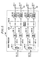
- TEST_PS A functional block diagram of driver processor 240 is shown in FIG.
- 5 includes one-shot multivibrators 240-5 and 240-10, a plurality of other one-shot circuits 240-15, -20, -25 and-30, buffer driver 240-35 and switch drivers 240-40, -45, -50 and -55.
- one-shot MV 240-5 switches to an active state for a duration of time ⁇ , e.g., a period of time greater than a so-called hold-over delay that is generated by pulse width detector 375, FIG. 2.
- the value of ⁇ is set to four seconds to ensure that the value of ⁇ will be greater than the hold-over delay, even if the delay is increased somewhat.
- the high going pulse on lead 240-51 triggers one-shot 240-15 which outputs a positive going pulse having a duration of, for example, twenty milliseconds, to buffer/driver 240-35, which similarly provides a buffer function between one-shot 240-15 and switch 240-40.
- switch 230 (S1) operates it disrupts the signal carried over path 25, thereby causing the opposite end node, e.g., node 150, to declare a LOS over path 25 and switch to the protection path.
- one-shot 240-15 returns to its original state, thereby causing switch driver 240-40 to release.
- Optical switch 230 remains operated.
- the Q and Q outputs of one-shot MV 240-5 return to their original (or opposite) logic states, which means that the Q output extending to one shot 240-20 via lead 240-52 returns to a high level e.g., +5 volts.
- the positive going transition at Q causes one-shot 240-20 to change state and output a positive pulse having a duration of, for example, twenty milliseconds. That output pulse is similarly buffered by buffer/driver 240-35 and then extended to switch driver 240-45 causing driver 240-45 to operate and reset switch 230 and return switch 230 to its original state. At the end of twenty milliseconds, one-shot 240-20 returns to its original state, thereby releasing switch driver 240-45.
- one-shot MV 240-10, one-shot circuits 240-25 and 240-35, buffer/driver 240-35 and switch drivers 240-50 and 240-55 cooperate in a similarly manner when (a) a LOS has been detected on the protection path, (b) that path is in service (i.e., has been connected to path 48) and (c) the service path (25 and 26) is available for service, as determined by the foregoing.
- switch driver 240-50 operates for twenty milliseconds and, in turn, operates optical switch 235 (S2) to disrupt the signal carried over protection path 30 and, thus cause the opposite end, e.g., node 150, to switch to the original service line.
- switch driver 240-55 will similarly operate for twenty milliseconds and reset optical switch 235.
- interference filter 315 may be, for example, Fabry-Perot etalon, fiber grating, etc.
- the foregoing was discussed in the context of what is commonly referred to as a 1+1 protection switching system. It is clear that the LOS detector may be readily used in other types of protection switching systems, for example, a 1 x N protection switching system, in which one protection line/path protects anyone of N active lines, where N > 1.
Landscapes
- Engineering & Computer Science (AREA)
- Computer Networks & Wireless Communication (AREA)
- Signal Processing (AREA)
- Physics & Mathematics (AREA)
- Electromagnetism (AREA)
- Optical Communication System (AREA)
- Optical Modulation, Optical Deflection, Nonlinear Optics, Optical Demodulation, Optical Logic Elements (AREA)
- Monitoring And Testing Of Exchanges (AREA)
- Use Of Switch Circuits For Exchanges And Methods Of Control Of Multiplex Exchanges (AREA)
Applications Claiming Priority (2)
| Application Number | Priority Date | Filing Date | Title |
|---|---|---|---|
| US08/994,213 US6266168B1 (en) | 1997-12-19 | 1997-12-19 | Optical protection switch employing an interference filter |
| US994213 | 1997-12-19 |
Publications (3)
| Publication Number | Publication Date |
|---|---|
| EP0926846A2 true EP0926846A2 (de) | 1999-06-30 |
| EP0926846A3 EP0926846A3 (de) | 1999-10-20 |
| EP0926846B1 EP0926846B1 (de) | 2001-11-14 |
Family
ID=25540405
Family Applications (1)
| Application Number | Title | Priority Date | Filing Date |
|---|---|---|---|
| EP98309974A Expired - Lifetime EP0926846B1 (de) | 1997-12-19 | 1998-12-04 | Optischer Schutzschalter mit einem Interferenzfilter |
Country Status (5)
| Country | Link |
|---|---|
| US (1) | US6266168B1 (de) |
| EP (1) | EP0926846B1 (de) |
| JP (1) | JP3734631B2 (de) |
| CA (1) | CA2252209C (de) |
| DE (1) | DE69802495T2 (de) |
Cited By (2)
| Publication number | Priority date | Publication date | Assignee | Title |
|---|---|---|---|---|
| WO2004062139A3 (en) * | 2002-12-23 | 2004-08-26 | Intel Corp | A multi-input variable gain amplifier |
| EP1363416A3 (de) * | 2002-05-15 | 2005-02-02 | Matsushita Electric Industrial Co., Ltd. | Optisches Übertragungssystem für eine Kabelfernsehaufwärtsrichtung |
Families Citing this family (27)
| Publication number | Priority date | Publication date | Assignee | Title |
|---|---|---|---|---|
| DE19906862A1 (de) * | 1999-02-18 | 2000-08-24 | Siemens Ag | Netzknoten mit optischen Add/Drop-Modulen |
| US6968130B1 (en) * | 1999-09-07 | 2005-11-22 | Nokia Corporation | System and method for fully utilizing available optical transmission spectrum in optical networks |
| IL132726A (en) * | 1999-11-03 | 2003-07-31 | Eci Telecom Ltd | Method and system for transmitting optical communication |
| AU2001268034A1 (en) * | 2000-03-10 | 2001-09-17 | Corning Incorporated | Devices and methods for controlling protection switching in an optical channel shared protection ring |
| JP2001268011A (ja) * | 2000-03-21 | 2001-09-28 | Fujitsu Ltd | 光ノードシステム、及び、スイッチの接続方法 |
| US6321004B1 (en) | 2001-04-24 | 2001-11-20 | Seneca Networks | Protection switching in bidirectional WDM optical communication networks |
| US6563979B2 (en) * | 2001-06-22 | 2003-05-13 | Dorsal Networks, Inc. | Automatically switched redundant switch configurations |
| US7075712B2 (en) * | 2002-05-30 | 2006-07-11 | Fujitsu Limited | Combining and distributing amplifiers for optical network and method |
| US7085496B2 (en) | 2002-05-30 | 2006-08-01 | Fujitsu Limited | Passive add/drop amplifier for optical networks and method |
| WO2004008833A2 (en) * | 2002-07-24 | 2004-01-29 | Ciena Corporation | Method and system for providing protection in an optical communication network |
| US7181137B1 (en) * | 2002-09-30 | 2007-02-20 | Cisco Technology, Inc. | Subband spectrum analysis for optical multiplex section protection |
| JP3974018B2 (ja) * | 2002-11-13 | 2007-09-12 | 富士通株式会社 | 可変光フィルタおよびそれを用いた光伝送システム、並びに、可変光フィルタの制御方法 |
| US7233738B2 (en) | 2003-02-18 | 2007-06-19 | Tyco Telecommunications (Us) Inc. | Protection switching architecture and method of use |
| US7499646B2 (en) * | 2004-02-23 | 2009-03-03 | Dynamic Method Enterprises Limited | Fast fault notifications of an optical network |
| US7474850B2 (en) * | 2004-02-23 | 2009-01-06 | Dynamic Method Enterprises Limited | Reroutable protection schemes of an optical network |
| US7941048B2 (en) * | 2007-06-29 | 2011-05-10 | Alcatel-Lucent Usa Inc. | Loss of signal detection |
| US8078052B2 (en) * | 2007-10-18 | 2011-12-13 | Cisco Technology, Inc. | Protocol-less all-optical 1+1 bidirectional revertive linear protection system |
| CN106656320B (zh) | 2015-10-29 | 2019-04-12 | 阿里巴巴集团控股有限公司 | 用于光量子通信业务的光纤信道损耗测量系统、方法及装置 |
| US10476587B2 (en) * | 2016-05-31 | 2019-11-12 | Alibaba Group Holding Limited | System and method for enhancing reliability in a transport network |
| CN108631875A (zh) | 2017-03-24 | 2018-10-09 | 阿里巴巴集团控股有限公司 | 双通道小型化可插拔模块、外壳和通信系统 |
| US11394814B2 (en) | 2020-05-20 | 2022-07-19 | Alibaba Group Holding Limited | Path control by end hosts in networks |
| US11057113B1 (en) | 2020-06-02 | 2021-07-06 | Alibaba Group Holding Limited | High-speed silicon photonics optical transceivers |
| US11668590B2 (en) | 2020-11-11 | 2023-06-06 | Alibaba Group Holding Limited | System and method for fiber sensing |
| US11336376B1 (en) | 2021-01-29 | 2022-05-17 | Alibaba Group Holding Limited | Flexible switch solution based on co-packaged optics |
| US11630261B2 (en) | 2021-04-29 | 2023-04-18 | Alibaba Singapore Holding Private Limited | Co-packaged optics switch solution based on analog optical engines |
| CN119544640A (zh) * | 2024-03-22 | 2025-02-28 | 北京字跳网络技术有限公司 | 用于转发数据的设备、方法、装置和存储介质 |
| CN121750097A (zh) * | 2024-09-26 | 2026-03-27 | 华为技术有限公司 | 一种光放大器、光通信系统和光放大方法 |
Family Cites Families (2)
| Publication number | Priority date | Publication date | Assignee | Title |
|---|---|---|---|---|
| US5680235A (en) | 1995-04-13 | 1997-10-21 | Telefonaktiebolaget Lm Ericsson | Optical multichannel system |
| JPH11508427A (ja) | 1995-06-26 | 1999-07-21 | テレフオンアクチーボラゲツト エル エム エリクソン(パブル) | 自己回復網 |
-
1997
- 1997-12-19 US US08/994,213 patent/US6266168B1/en not_active Expired - Lifetime
-
1998
- 1998-10-29 CA CA002252209A patent/CA2252209C/en not_active Expired - Fee Related
- 1998-12-04 DE DE69802495T patent/DE69802495T2/de not_active Expired - Lifetime
- 1998-12-04 EP EP98309974A patent/EP0926846B1/de not_active Expired - Lifetime
- 1998-12-18 JP JP35987898A patent/JP3734631B2/ja not_active Expired - Fee Related
Cited By (5)
| Publication number | Priority date | Publication date | Assignee | Title |
|---|---|---|---|---|
| EP1363416A3 (de) * | 2002-05-15 | 2005-02-02 | Matsushita Electric Industrial Co., Ltd. | Optisches Übertragungssystem für eine Kabelfernsehaufwärtsrichtung |
| US7603693B2 (en) | 2002-05-15 | 2009-10-13 | Panasonic Corporation | CATV uplink optical transmission system |
| WO2004062139A3 (en) * | 2002-12-23 | 2004-08-26 | Intel Corp | A multi-input variable gain amplifier |
| US7212041B2 (en) | 2002-12-23 | 2007-05-01 | Intel Corporation | Weighted multi-input variable gain amplifier |
| CN100483989C (zh) * | 2002-12-23 | 2009-04-29 | 英特尔公司 | 多输入可变增益放大器 |
Also Published As
| Publication number | Publication date |
|---|---|
| US6266168B1 (en) | 2001-07-24 |
| CA2252209A1 (en) | 1999-06-19 |
| DE69802495D1 (de) | 2001-12-20 |
| CA2252209C (en) | 2002-09-03 |
| JP3734631B2 (ja) | 2006-01-11 |
| EP0926846B1 (de) | 2001-11-14 |
| JPH11275615A (ja) | 1999-10-08 |
| EP0926846A3 (de) | 1999-10-20 |
| DE69802495T2 (de) | 2002-06-27 |
Similar Documents
| Publication | Publication Date | Title |
|---|---|---|
| CA2252209C (en) | Optical protection switch employing an interference filter | |
| US6421149B2 (en) | Protection in an optical telecommunications system | |
| US5870212A (en) | Self-healing optical network | |
| EP0372711B1 (de) | Betriebssicheres optisches Übertragungssystem | |
| US6075629A (en) | Optical protection switch employing an interference filter | |
| US7953321B2 (en) | Optical transmission equipment and optical add-drop multiplexer | |
| EP0973354A2 (de) | Optisches Übertragungssystem mit Optischer Wiederherstellung | |
| US6414771B2 (en) | Optical transmission system including optical restoration | |
| US7660526B2 (en) | Through channel loss prevention at a WDM node | |
| US6639703B1 (en) | Receiver transponder for protected networks | |
| SG11202113035QA (en) | Optical source switching method and apparatus | |
| EP1486014B1 (de) | Optischer schalter mit optischer versorgung und steuerung | |
| KR100319744B1 (ko) | 파장선택형광검출기를이용한파장분할다중화된광신호의채널정보검출장치및그방법 | |
| US7283742B2 (en) | Optical signal judging system and optical signal judging method | |
| EP0874481A2 (de) | Optisches Teilnehmer-Anschlussnetzsystem | |
| JP2000236298A (ja) | 自動分散補償回路及びそれを用いた光伝送システム | |
| KR100586747B1 (ko) | 수동 광 네트워크의 광모듈 보호구조 | |
| KR950022462A (ko) | 고장 감내형 광 링 통신망(A fault-tolerant optical ring network) | |
| KR20050062322A (ko) | 파장분할 다중화 수동형 광 네트워크에서의 링크 보호장치 및 그 방법 | |
| JP2000031906A (ja) | 光波長多重中継器 |
Legal Events
| Date | Code | Title | Description |
|---|---|---|---|
| PUAI | Public reference made under article 153(3) epc to a published international application that has entered the european phase |
Free format text: ORIGINAL CODE: 0009012 |
|
| 17P | Request for examination filed |
Effective date: 19981224 |
|
| AK | Designated contracting states |
Kind code of ref document: A2 Designated state(s): DE FR IT |
|
| AX | Request for extension of the european patent |
Free format text: AL;LT;LV;MK;RO;SI |
|
| PUAL | Search report despatched |
Free format text: ORIGINAL CODE: 0009013 |
|
| AK | Designated contracting states |
Kind code of ref document: A3 Designated state(s): AT BE CH CY DE DK ES FI FR GB GR IE IT LI LU MC NL PT SE |
|
| AX | Request for extension of the european patent |
Free format text: AL;LT;LV;MK;RO;SI |
|
| RIC1 | Information provided on ipc code assigned before grant |
Free format text: 6H 04B 10/08 A, 6H 04B 10/24 B, 6H 04J 14/02 B, 6H 04B 10/00 B |
|
| AKX | Designation fees paid |
Free format text: DE FR IT |
|
| 17Q | First examination report despatched |
Effective date: 20000608 |
|
| GRAG | Despatch of communication of intention to grant |
Free format text: ORIGINAL CODE: EPIDOS AGRA |
|
| GRAG | Despatch of communication of intention to grant |
Free format text: ORIGINAL CODE: EPIDOS AGRA |
|
| GRAH | Despatch of communication of intention to grant a patent |
Free format text: ORIGINAL CODE: EPIDOS IGRA |
|
| GRAH | Despatch of communication of intention to grant a patent |
Free format text: ORIGINAL CODE: EPIDOS IGRA |
|
| GRAA | (expected) grant |
Free format text: ORIGINAL CODE: 0009210 |
|
| AK | Designated contracting states |
Kind code of ref document: B1 Designated state(s): DE FR IT |
|
| PG25 | Lapsed in a contracting state [announced via postgrant information from national office to epo] |
Ref country code: IT Free format text: LAPSE BECAUSE OF FAILURE TO SUBMIT A TRANSLATION OF THE DESCRIPTION OR TO PAY THE FEE WITHIN THE PRESCRIBED TIME-LIMIT;WARNING: LAPSES OF ITALIAN PATENTS WITH EFFECTIVE DATE BEFORE 2007 MAY HAVE OCCURRED AT ANY TIME BEFORE 2007. THE CORRECT EFFECTIVE DATE MAY BE DIFFERENT FROM THE ONE RECORDED. Effective date: 20011114 |
|
| REF | Corresponds to: |
Ref document number: 69802495 Country of ref document: DE Date of ref document: 20011220 |
|
| PLBE | No opposition filed within time limit |
Free format text: ORIGINAL CODE: 0009261 |
|
| STAA | Information on the status of an ep patent application or granted ep patent |
Free format text: STATUS: NO OPPOSITION FILED WITHIN TIME LIMIT |
|
| 26N | No opposition filed | ||
| REG | Reference to a national code |
Ref country code: FR Ref legal event code: CD Owner name: ALCATEL-LUCENT USA INC. Effective date: 20131122 |
|
| REG | Reference to a national code |
Ref country code: FR Ref legal event code: GC Effective date: 20140410 |
|
| REG | Reference to a national code |
Ref country code: FR Ref legal event code: RG Effective date: 20141015 |
|
| REG | Reference to a national code |
Ref country code: FR Ref legal event code: PLFP Year of fee payment: 18 |
|
| PGFP | Annual fee paid to national office [announced via postgrant information from national office to epo] |
Ref country code: DE Payment date: 20151211 Year of fee payment: 18 |
|
| PGFP | Annual fee paid to national office [announced via postgrant information from national office to epo] |
Ref country code: FR Payment date: 20151221 Year of fee payment: 18 |
|
| REG | Reference to a national code |
Ref country code: DE Ref legal event code: R119 Ref document number: 69802495 Country of ref document: DE |
|
| REG | Reference to a national code |
Ref country code: FR Ref legal event code: ST Effective date: 20170831 |
|
| PG25 | Lapsed in a contracting state [announced via postgrant information from national office to epo] |
Ref country code: FR Free format text: LAPSE BECAUSE OF NON-PAYMENT OF DUE FEES Effective date: 20170102 |
|
| PG25 | Lapsed in a contracting state [announced via postgrant information from national office to epo] |
Ref country code: DE Free format text: LAPSE BECAUSE OF NON-PAYMENT OF DUE FEES Effective date: 20170701 |