EP0929083B1 - Widerstand und sein Herstellungsverfahren - Google Patents
Widerstand und sein Herstellungsverfahren Download PDFInfo
- Publication number
- EP0929083B1 EP0929083B1 EP99100262A EP99100262A EP0929083B1 EP 0929083 B1 EP0929083 B1 EP 0929083B1 EP 99100262 A EP99100262 A EP 99100262A EP 99100262 A EP99100262 A EP 99100262A EP 0929083 B1 EP0929083 B1 EP 0929083B1
- Authority
- EP
- European Patent Office
- Prior art keywords
- top electrode
- layer
- resistor
- substrate
- conductive powder
- Prior art date
- Legal status (The legal status is an assumption and is not a legal conclusion. Google has not performed a legal analysis and makes no representation as to the accuracy of the status listed.)
- Expired - Lifetime
Links
Images


Classifications
-
- H—ELECTRICITY
- H01—ELECTRIC ELEMENTS
- H01C—RESISTORS
- H01C17/00—Apparatus or processes specially adapted for manufacturing resistors
- H01C17/28—Apparatus or processes specially adapted for manufacturing resistors adapted for applying terminals
- H01C17/281—Apparatus or processes specially adapted for manufacturing resistors adapted for applying terminals by thick film techniques
-
- H—ELECTRICITY
- H01—ELECTRIC ELEMENTS
- H01C—RESISTORS
- H01C1/00—Details
- H01C1/14—Terminals or tapping points specially adapted for resistors; Arrangements of terminals or tapping points on resistors
- H01C1/142—Terminals or tapping points specially adapted for resistors; Arrangements of terminals or tapping points on resistors the terminals or tapping points being coated on the resistive element
-
- H—ELECTRICITY
- H01—ELECTRIC ELEMENTS
- H01C—RESISTORS
- H01C17/00—Apparatus or processes specially adapted for manufacturing resistors
- H01C17/006—Apparatus or processes specially adapted for manufacturing resistors adapted for manufacturing resistor chips
-
- H—ELECTRICITY
- H05—ELECTRIC TECHNIQUES NOT OTHERWISE PROVIDED FOR
- H05K—PRINTED CIRCUITS; CASINGS OR CONSTRUCTIONAL DETAILS OF ELECTRIC APPARATUS; MANUFACTURE OF ASSEMBLAGES OF ELECTRICAL COMPONENTS
- H05K3/00—Apparatus or processes for manufacturing printed circuits
- H05K3/30—Assembling printed circuits with electric components, e.g. with resistors
- H05K3/32—Assembling printed circuits with electric components, e.g. with resistors electrically connecting electric components or wires to printed circuits
- H05K3/34—Assembling printed circuits with electric components, e.g. with resistors electrically connecting electric components or wires to printed circuits by soldering
- H05K3/341—Surface mounted components
- H05K3/3431—Leadless components
- H05K3/3442—Leadless components having edge contacts, e.g. leadless chip capacitors, chip carriers
Definitions
- the present invention relates to the field of resistors and their manufacturing methods which allow the high density mounting of resistors on printed wiring boards used for electronic equipment.
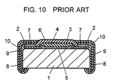
- Fig. 10. is a sectional view of a resistor of the prior art.
- a first top electrode layer 2 is disposed on both left and right ends of the top face of an insulated substrate 1.
- a resistance layer 3 is disposed on the insulated substrate 1 so as to partially overlap the first top electrode layer 2.
- a first protective layer 4 is disposed to cover only the entire face of the resistance layer 3.
- a trimming groove 5 is provided on the resistance layer 3 and the first protective layer 4 so as to adjust the resistance value.
- a second protective layer 6 is disposed on the top face of the first protective layer 4.
- a second top electrode layer 7 is disposed on the top face of the first top electrode layer 2 stretching to the full width of the insulated substrate 1.
- a side electrode layer 8 is disposed on a side face of the insulated substrate 1.
- a nickel layer 9 and solder layer 10 are disposed on the surface of the second top electrode layer 7 and the side electrode layer 8.
- the height of the solder layer 10 is lower than that of the second protective layer 6.
- the second protective layer 6 of the resistor of the prior art generally protrudes from the entire resistor.
- Figs 11A to 11F are perspective views of the resistor illustrating how the resistor of the prior art is manufactured.
- the first top electrode layer 2 is applied and formed on both left and right ends of the top face of the insulated substrate 1.
- the resistance layer 3 is then applied and formed on the top face of the insulated substrate 1 so as to partially overlap the first top electrode layer 2.
- Fig. 11B shows that
- the trimming groove 5 is provided on the resistance layer 3 and the first protective layer 4 by means such as a laser beam to adjust the resistance value of the resistance layer 3 to within a specified allowable resistance.
- the second protective layer 6 is applied and formed only on the top face of the first protective layer 4.
- the second top electrode layer 7 is then applied and formed on the top face of the first top electrode layer 2, stretching to the full width of the insulated substrate 1 (Fig. 11E).
- the side electrode layer 8 is applied and formed on the first top electrode layer 2 and the left and right side faces of the insulated substrate 1 so as to electrically connect with the first top electrode layer 2 and the second top electrode layer 7.
- the surfaces of the second top electrode layer 7 and the side electrode layer 8 are plated with nickel, and then soldered to form the nickel layer and solder layer 10, as shown in Fig. 10, completing the manufacture of the resistor of the prior art.
- a resistor and its manufacturing method is known from EP 0810614.
- a resistor of the present invention is provided which is defined by the features of claim 1. It comprises a substrate, a pair of first top electrode layers disposed on the top face of the substrate, a resistance layer disposed so as to electrically connect with the first top electrode layers, a protective layer disposed so as to cover at least the resistance layer, and a pair of second top electrode layers disposed at least on the top faces of each first top electrode layer. At least one of the pairs of first top electrode layers and second top electrode layers extends to a portion of the side face of the substrate.
- a method for manufacturing a resistor of the present invention is defined by the features of claim 26. It comprises the steps of disposing the first top electrode layers at least on the top face of a sheet substrate having a division slit, disposing the resistance layer so as to electrically connect between the first top electrode layers, disposing the protective layer so as to cover at least the top face of the resistance layer, and disposing the second top electrode layers so as to electrically connect with at least the first top electrode layers; and the steps of dividing the sheet substrate along the division slit into a substrate strips, and dividing the substrate strips into substrate pieces. At least one of the pairs of first top electrode layers and the second top electrode layers is formed to cover the division slit by applying an electrode paste to fill inside the division slits.
- a resistor is soldered to a printed wiring board by the top electrode and the side electrode disposed on a portion of the side face of the substrate when the resistor is mounted on the printed wiring board. This enables a reduction in the area required for forming a solder fillet, resulting in the reduction of the mounting area including the soldered area on a printed wiring board.
- Fig. 1 is a section view of a resistor in accordance with a first exemplary embodiment of the present invention.
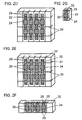
- Figs 2A to 2G are perspective views of an exemplary resistor at various stages of manufacture on a sheet substrate, illustrating an exemplary method for manufacturing a resistor in accordance with the first exemplary embodiment.
- Fig. 3A is a section view of a mounted resistor in accordance with the first exemplary embodiment of the present invention.
- Fig. 3B is a top view of the mounted resistor in accordance with the first exemplary embodiment of the present invention.
- Fig. 4 is a section view of a resistor in accordance with a second exemplary embodiment of the present invention.
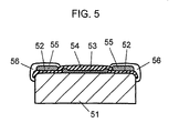
- Fig. 5 is a section view of a resistor in accordance with a third exemplary embodiment of the present invention.
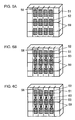
- Figs 6A to 6G are perspective views of an exemplary resistor at various stages of manufacture on a sheet substrate, illustrating an exemplary method for manufacturing a resistor in accordance with the third exemplary embodiment.
- Fig. 7A is a section view of a mounted resistor in accordance with the third exemplary embodiment of the present invention.
- Fig. 7B is a top view of the mounted resistor in accordance with the third exemplary embodiment of the present invention.
- Fig. 8 is a section view of a resistor in accordance with a fourth exemplary embodiment of the present invention.
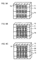
- Figs 9A to 9G are perspective views of an exemplary resistor at various stages of manufacture on a sheet substrate, illustrating an exemplary method for manufacturing a resistor in accordance with the fourth exemplary embodiment.
- Fig. 10 is a section view of a resistor of the prior art.
- Figs. 11A to 11F are process flow charts illustrating a method for manufacturing the resistor in accordance with the prior art.
- Fig. 12A is a section view of a mounted resistor of the prior art.
- Fig. 12B is a top view of the mounted resistor of the prior art.
- a resistor and its manufacturing method of the present invention are explained with reference to Figs. 1 to 3B.
- the area of the second top electrode layer 25 formed on a part of the side face of the substrate 21 is half or smaller than the entire side face of the substrate 21.
- a clearance 26 is created between the protective layer 24 and the second top electrode layer 25.
- the first top electrode layers 22 have an exposed area at the clearance 26 which is neither covered by the protective layer 24 nor the second top electrode layer 25.
- a nickel layer 27 and solder layer 28 may be disposed on the second top electrode layer 25, as required, to secure quality such as reliability when the resistor is soldered.
- the exposed area of the first top electrode layers 22 and the nickel layer 27 are in direct electrical contact through the clearance 26.
- Figs. 2A to 2G illustrate an exemplary method for manufacturing a resistor in accordance with the first exemplary embodiment of the present invention.
- a sheet substrate 21, typically 96% aluminum, with good heat resistance and insulation, has more than one vertical division slit 29 and more than one horizontal division slit 30.
- an electrode paste typically containing glass frit and a conductive powder such as Ag
- the sheet substrate 21 is fired at approximately 850°C to form the first top electrode layer 22.
- the depth of the division slits 29 and 30 is half or less of the thickness of substrate 21 to prevent breakage due to handling during manufacturing.
- a resistance paste typically made mainly of ruthenium oxide, is printed so as to electrically connect with the first top electrode layers 22, and is fired at approximately 850°C to form the resistance layer 23.
- a trimming groove 31 is provided by means such as a YAG laser to adjust the resistance of the resistance layer 23 to a specified value.
- a trimming probe for measuring the resistance value may be placed on the first top electrode layer 22 before trimming.
- a resin paste typically made of epoxy resin, is printed so as to protect the adjusted resistance layer 23, and baked in a conveyor-type continuous curing furnace at approximately 200°C for approximately 30 minutes to thermally cure and form the protective layer 24.
- the protective layer 24 may be provided to cover more than one resistance layer 23 horizontally aligned, crossing the vertical division slit 29.
- an electrode paste made typically of conductive powder, such as Ag or Ni, and epoxy resin is screen printed on each of the first top electrode layers 22 of adjacent resistors in the vertical direction, crossing the horizontal division slit 30 of the sheet substrate 21 without overlapping the protective layer 24.
- the first top electrode layers 22 consequently have an exposed area 26 that is neither covered by the protective layer 24 nor the second top electrode layer 25.
- the substrate 21 is baked in a conveyor-type continuous curing furnace at approximately 200°C for approximately 30 minutes to thermally cure and form a second top electrode layer 25.
- the electrode paste fills the horizontal division slit 30 to form the second top electrode layer 25 to the bottom of the division slit.
- the second top electrode layer 25 may also be formed continuously on each of the first top electrode layers 22 of adjacent resistors in the horizontal direction, crossing the vertical division slit 29.
- the sheet substrate 21 is divided along the horizontal division slit 30 to create a substrate strip 32.
- the second top electrode layer 25 that filled into horizontal division slit 30, extends onto the divided face of the substrate strip 32.
- the substrate strip 32 is divided along the vertical division slit 29 to create a substrate piece 33.
- nickel layer 27 as a middle layer and a solder layer 28 as an outermost layer are electroplated in turn on an exposed surface of the second top electrode layer 25, completing the manufacture of the resistor of the present exemplary embodiment.
- Figs. 3A and 3B show a resistor, manufactured using the above steps, mounted on a printed wiring board.
- the surface of the resistor where the protective layer 24 is formed faces down for mounting.
- the first top electrode layer 22 and the second top electrode layer 25, including the side electrode portion of the second top electrode layer 25 that extends to the side face of the substrate as shown in Fig. 2, are all soldered.
- an extremely small fillet 34 is formed since the area of the side electrode portion of electrode layer 25 is small, an extremely small fillet 34, compared with that needed for a resistor of the prior art, is formed.
- a total of a resistor area 35 and a resistor side face area 36 required for soldering the resistor is the mounting area 37.
- the resistor in the first exemplary embodiment enables reduction of the mounting area by 20% compared to the configuration of a conventional resistor.
- the present invention requires only a small area for forming a fillet when soldering the resistor onto a printed wiring board because the area of the side electrode of the resistor is small, enabling reduction of the mounting area.
- the second top electrode layer is made of a conductive paste consisting of a conductive powder and epoxy resin. If Ag is used as a conductive powder, its conductive resistance is as high as approximately 10 -4 ⁇ cm, and approximately 10 -2 ⁇ cm when nickel is used as conductive powder (approximately 10 -6 ⁇ cm when nickel plating or Ag grazed material are used). Accordingly, variations in the thickness when forming the second top electrode layer result in variations in resistance value of the resistor, because the conductive resistance value is added to the specified resistance. However, as shown in Fig.
- the resistor is not affected by the second top electrode layer 25 which has high conductive resistance, because any exposed area of the first top electrode layer 22 and the nickel layer 27, which has low conductive resistance, are in direct electrical contact at the clearance 26. This results in the reliable manufacture of a highly accurate resistor.
- the first exemplary embodiment describes first top electrode layer 22 and nickel layer 27 as being in direct electrical contact. However, this is not intended as a limitation to the nickel layer. The same effect is achievable by placing the solder layer and the first top electrode layer 22 in direct electrical contact, or by using a material with low conductive resistance that does not affect the resistance value of the resistor.
- the first exemplary embodiment preferably uses ruthenium oxide grazed material as the resistance layer 23.
- the material used for the resistance layer is not limited to ruthenium oxide grazed material.
- the same effect is achievable by the use of nichrome thin film material for the resistance layer.
- the first exemplary embodiment By making the surface of solder layer 28 level with or higher than the surface of protective layer 24, the first exemplary embodiment also improves mounting quality by preventing generation of a space between the solder layer 28 and the land (not illustrated) of the printed wiring board.
- the first exemplary embodiment also enables the further reduction of the mounting area by eliminating the creation of the side electrode and not forming a fillet when soldering the resistor to the printed wiring board. However, if no fillet is formed, automated inspection using image recognition may become less effective. Accordingly, it is preferable to form a fillet even it is small.
- Table 1 shows the effects (improved characteristics) achieved by the combination of materials used for the first top electrode layer 22, protective layer 24, and second top electrode layer 25.
- Protective layer 24 Improved characteristics 1 Ag conductive powder + Glass (Baked at 850°C) Ag conductive powder + Resin (Cured at 200°C) Resin system (Cured at 200°C) Low treatment temperature for the protective layer 24 prevents changes in a resistance value in the process, reducing deviations in the resistance of products.
- a resistor in accordance with a second exemplary embodiment of the present invention is explained with reference to Fig. 4.
- a pair of first top electrode layers 42 are disposed on both ends of the main surface of a substrate 41, typically made of 96% aluminum.
- a resistance layer 43 typically constituted mainly of ruthenium oxide, is formed so as to electrically connect with the first top electrode layers 42.
- a protective layer 44 typically made of epoxy resin, is disposed on the top face of the resistance layer 43.
- a second top electrode layer 45 typically a mixture of epoxy resin and a conductive powder such as Ag, is disposed on the top face of the first top electrode layers 42 and a part of the side face of the substrate 41.
- the area of the second top electrode layer 45 on the side face of the substrate 41 is half or smaller than the entire side face of the substrate 41.
- a window 46 is created on the second top electrode layer 45.
- the first top electrode layers 42 have an exposed area, at the window 46, which is neither covered by the protective layer 44 nor the second top electrode layer 45.
- a nickel layer 47 and solder layer 48 may be disposed on the second top electrode layer 45, as required, to secure quality such as reliability when the resistor is soldered.
- the first top electrode layers 42 and nickel layer 47 are in direct electrical contact through the window 46.
- Points in a method for manufacturing the resistor in this exemplary embodiment different from the first exemplary embodiment is that a screen printing mask is used for forming the second top electrode layer 45 in order to create the window 46. Other steps are the same as the first exemplary embodiment.
- a resistor and its manufacturing method in accordance with a third exemplary embodiment of the present invention are explained with reference to Figs. 5 to 7B.
- a pair of first top electrode layers 52 are disposed on both ends of the top face and a part of the side face of a substrate 51, typically made of 96% aluminum.
- An area of the first top electrode layers 52 on the side face of the substrate 51 is half or less of the entire side face of the substrate 51.
- a resistance layer 53 typically made mainly of ruthenium oxide, is disposed so as to electrically connect with the pair of first top electrode layers 52.
- a protective layer 54 typically made mainly of glass is disposed so as to cover at least the top face of the resistance layer 53.
- a second top electrode layer 55 typically a mixture of glass frit and a conductive powder such as Cu, is disposed on the top face of the first top electrode layers 52. An edge of the second top electrode layer 55 is curved. A solder layer 56 is electroplated so as to cover at least an exposed top face of the second top electrode layer 55.
- a sheet substrate 51 typically 96% aluminum, with good heat resistance and insulation, has more than one vertical division slit 58 and horizontal division slit 59 on its surface.
- An electrode paste typically containing glass frit and a conductive powder such as Ag, is printed, crossing and filling inside the horizontal division slit 59, and is fired at approximately 850°C to form the first top electrode layer 52. Since the electrode paste fills the horizontal division slit 59, the first top electrode layer 52 is formed to the bottom of the division slit.
- the depth of the division slits 58 and 59 is half or less of the thickness of the substrate 51 to prevent breakage due to handling during manufacturing.
- a resistance paste typically made mainly of ruthenium oxide, is printed so as to electrically connect with the first top electrode layers 52, and fired at approximately 850°C to form the resistance layer 53.
- a trimming groove 60 is provided by means such as a YAG laser to adjust the resistance of the resistance layer 53 to a specified value.
- a trimming probe for measuring the resistance value may be placed on the first top electrode layers 52 before trimming.
- a paste typically made mainly of glass is printed to protect the adjusted resistance layer 53, and fired at approximately 600°C to form a protective layer 54.
- the protective layer 54 may be provided to cover all of more than one resistance layer 53 horizontally aligned, crossing the vertical division slit 58.
- an electrode paste typically containing a mixture of glass frit and a conductive powder such as Cu, is printed on the top face of the first top electrode layer 52 without crossing the horizontal division slit 59, and fired at approximately 600°C in the nitrogen ambient to form a second top electrode layer 55.
- the second top electrode layer 55 may be formed continuously over each of the first top electrode layers 52 of adjacent resistors in the horizontal direction, crossing the vertical division slit 58.
- the sheet substrate 51 is divided along the horizontal division slit 59 to create a substrate strip 61.
- the first top electrode layer 52 that filled into horizontal division slit 59 extends onto the divided face of the substrate strip 61.
- the substrate strip 61 is divided along the vertical division slit 58 to create a substrate piece 62.
- Solder is electroplated on an exposed surface area of the first top electrode layers 52 and the second top electrode layer 55 to create a solder layer 56, as shown in Fig. 5, completing the manufacture of the resistor in this exemplary embodiment.
- Figs. 7A and 7B show the resistor in the third exemplary embodiment mounted on a printed wiring board. It is apparent that the surface of the resistor where the protective layer 54 is formed is facing down for mounting.
- the second top electrode layer 55 and the side electrode which is a part of the first top electrode layer 52 extending to the side face of the substrate 51, as shown in Fig. 5, are all soldered. It should be noted that since the area of the side electrode (Fig. 5) is small, an extremely small fillet 63, compared with that needed for a resistor of the prior art is formed. Accordingly, as shown in Fig. 7B, the total mounting area 66 required for soldering the resistor includes a resistor area 64 and a resistor side face area corresponding to land 65. When a square chip resistor of 0.6 mm x 0.3 mm is used, the resistor in the third exemplary embodiment enables reduction of the mounting area by approximately 20%, compared to the configuration of the conventional resistor.
- the present invention requires only a small area for forming a fillet when soldering the resistor onto a printed wiring board because the area of the side electrode of the resistor is small, enabling reduction of the mounting area.
- the third exemplary embodiment By making the surface of the solder layer 56 level with or higher than and the surface of protective layer 54, the third exemplary embodiment also improves mounting quality by preventing generation of space between the solder layer 56 and the land 65 of the printed wiring board.
- the third exemplary embodiment also enables the further reduction of the mounting area by eliminating the creation of the side electrode and not forming a fillet when soldering the resistor onto a printed wiring board. However, if no fillet is formed, automated inspection using image recognition may become less effective. Accordingly, it is preferable to form a fillet even it is small.
- Table 2 and 3 show the effects (improved characteristics) achieved by changing the combination of materials used for the first top electrode layers 52, protective layer 54, and second top electrode layer 55.
- Protective layer 54 Improved characteristics 1 Ag conductive powder + Glass (Baked at 850°C) Ag Pd conductive powder + Glass (Baked at 600°C) Glass system (Cured at 600°C) Baking of the second top electrode layer in air enables manufacture of the resistor less expensively. 2 Ag conductive powder + Glass (Baked at 850°C) Ni conductive powder + resin (Baked at 600°C) Glass system (Cured at 600°C) In addition to the characteristics of the combination 1, the use of Ni for the electrode enables manufacture of the resistor less expensively.
- a resistor and its manufacturing method in accordance with a fourth exemplary embodiment of the present invention are explained with reference to Figs. 8 to 9G.
- a pair of first top electrode layers 72 are disposed on both ends of the top face of a substrate 71, typically 96% aluminum.
- a resistance layer 73 typically made mainly of ruthenium oxide, is disposed so as to electrically connect with the first top electrode layers 72.
- a protective layer 74 typically made mainly of glass, is disposed so as to cover the top face of the resistance layer 73.
- a second top electrode layer 75 typically containing glass frit and a conductive powder such as Cu, is disposed on the top face of the first top electrode layer 72 and a part of the side face of the substrate 71.
- a part of the second top electrode layer 75 on the side face of the substrate 71 is half or less of the entire side face of the substrate 71.
- An edge of the second top electrode layer 75 is curved, and its exposed top face is covered with a solder layer 76.
- more than one vertical division slit 78 and horizontal division slit 79 are provided on the surface of the sheet substrate 71, typically made of 96% aluminum with good heat resistance and insulation.
- An electrode paste typically containing glass frit and a conductive powder such as Ag, is printed on both sides of the horizontal division slit 79 without crossing the horizontal division slit 79, and fired at approximately 850°C to form a first top electrode layers 72.
- the depths of division slits 78 and 79 are generally set to half or less of the thickness of substrate 71 so as to prevent breakage of the substrate by handling during manufacturing.
- a resistance paste typically made mainly of ruthenium oxide, is printed so as to electrically connect with the first top electrode layer 72, and fired at approximately 850°C to form the resistance layer 73.
- a trimming groove 80 is provided by means such as a YAG laser to adjust the resistance of the resistance layer 73 to a specified value.
- a trimming probe for measuring resistance may be placed on the first top electrode layers 72 before trimming.
- a paste typically made mainly of glass, is printed to protect the adjusted resistance layer 73, and fired at approximately 600°C to form the protective layer 74.
- the protective layer 74 may be formed over all of more than one resistance layer 73 horizontally aligned, crossing the vertical division slit 78.
- an electrode paste typically containing glass frit and a conductive powder such as Cu, is printed on the top face of each of the first top electrode layers of adjacent resistors in the vertical direction, crossing the horizontal division slit 79, and fired at approximately 600°C in the nitrogen ambient to form the second top electrode layer 75.
- the electrode paste fills the horizontal division slit 79 so that the second top electrode layer 75 is formed to the bottom of the division slit.
- the second top electrode layer 75 may be formed continuously on more than one first top electrode layer 72 horizontally aligned, crossing the vertical division slit 78.
- the sheet substrate 71 is divided along the horizontal division slit 79 to create a substrate strip 81. Since the second top electrode layer 75 is formed to the bottom of the horizontal division slit 79, the second top electrode layer 75 extends to the divided face of the substrate strip 81.
- the substrate strip 81 is divided along the vertical division slit 78 to create a substrate piece 82.
- Solder is electroplated on an exposed surface of the second top electrode layer 75 to form the solder layer 76,as shown in Fig. 8, completing the manufacture of the resistor in the fourth exemplary embodiment.
- the solder layer is formed by electroplating.
- dip soldering in a melted solder bath between approximately 200°C and approximately 250°C is also applicable.
- transfer printing of a paste material mainly made of tin or solder onto the second top electrode layer 75 and application of heat treatment at an ambient temperature of approximately 200°C to approximately 280°C is also feasible.
- Table 4 and 5 shows the effects (improved characteristics) achieved by changing the combination of materials for the first top electrode layer 72, protective layer 74, and second top electrode layer 75.
- Protective layer 74 Improved characteristics 14
- Baking of the second top electrode layer in air enables to manufacture the resistor less expensively.
- 15 Ag conductive powder + Glass (Baked at 850°C)
- Ni conductive powder + Glass (Baked at 600°C) Glass system (Cured at 600°C)
- the use of Ni for the electrode enables to manufacture the resistor more inexpensively.
Landscapes
- Engineering & Computer Science (AREA)
- Microelectronics & Electronic Packaging (AREA)
- Manufacturing & Machinery (AREA)
- Apparatuses And Processes For Manufacturing Resistors (AREA)
- Non-Adjustable Resistors (AREA)
- Details Of Resistors (AREA)
Claims (34)
- Widerstand umfassend:dadurch gekennzeichnet, dassein Substrat (21, 41, 51, 71) mit einer oberen Fläche und einer Mehrzahl von Seitenflächen;ein Paar von ersten oberen Elektrodenschichten (22, 42, 52, 72) wenigstens auf der oberen Fläche des Substrats (21, 41, 51, 71);eine Widerstandsschicht (23, 43, 53, 73), die über der oberen Fläche angeordnet ist, so dass sie mit den ersten oberen Elektrodenschichten (22, 42, 52, 72) elektrisch verbunden ist;eine Schutzschicht (24, 44, 54, 74), die derart angeordnet ist, dass sie wenigstens die Widerstandsschicht (23, 43, 53, 73) überdeckt; undein Paar von zweiten oberen Elektrodenschichten (25, 45, 55, 75), das über dem Paar von ersten oberen Elektrodenschichten (22, 42, 52, 72) wenigstens über der oberen Fläche des Substrats angeordnet ist;
wenigstens eines der Paare von ersten oberen Elektrodenschichten (22, 42, 52, 72) und zweiten oberen Elektrodenschichten (25, 45, 55, 75) sich erstreckt, so dass es teilweise an den Substratseitenflächen anhaftet. - Widerstand nach Anspruch 1, wobei jede der ersten oberen Elektrodenschichten (22, 42, 52, 72) eine bloßgelegte Fläche aufweist, der durch die Schutzschicht (24, 44, 54, 74) und die zweite obere Elektrodenschicht (25, 45, 55, 75) unbedeckt bleibt; und der Widerstand außerdem eine Überzugsschicht (27, 28, 47, 48, 56, 76) aufweist, die jede zweite obere Elektrodenschicht (25, 45, 55, 75) überdeckt.
- Widerstand nach Anspruch 1, wobei:das Paar von ersten oberen Elektrodenschichten (22, 42, 52, 72) nur auf der oberen Fläche des Substrats (21, 41, 51, 71) angeordnet ist;sich jede zweite obere Elektrodenschicht (25, 45, 55, 75) nach einem Teil der daran angrenzenden Seitenfläche des Substrats (21, 41, 51, 71) erstreckt; undder Widerstand weiterhin eine Überzugsschicht (27, 28, 47, 48, 56, 76) aufweist, die über der zweiten oberen Elektrodenschicht (25, 45, 55, 75) angeordnet ist, so dass die erste obere Elektrodenschicht (22, 42, 52, 72) und die Überzugsschicht (27, 28, 47, 48, 56, 76) in direktem elektrischen Kontakt stehen.
- Widerstand nach Anspruch 3, wobei ein Zwischenraum (26, 46) zwischen der Schutzschicht (24, 44, 54, 74) und jeder der zweiten oberen Elektrodenschichten (25, 45, 55, 75) definiert ist und der Zwischenraum (26, 46) einen bloßgelegten Teil von jeder ersten oberen Elektrodenschicht (22, 42, 52, 72) definiert, wobei der bloßgelegte Teil und die Überzugsschicht (27, 28, 47, 48, 56, 76) in direktem elektrischen Kontakt stehen.
- Widerstand nach Anspruch 3, wobei ein Fenster (26, 46) durch jede der zweiten oberen Elektrodenschichten (25, 45, 55, 75) über der oberen Fläche des Substrats (21, 41, 51, 71) gebildet ist und jedes Fenster (26, 46) einen bloßgelegten Teil von jeder ersten oberen Elektrodenschicht (22, 42, 52, 72) definiert und umgeben ist von der entsprechenden zweiten oberen Elektrodenschicht (25, 45, 55, 75), wobei der bloßgelegte Teil und die Überzugsschicht (27, 28, 47, 48, 56, 76) durch die entsprechende zweite obere Elektrodenschicht (25, 45, 55, 75) in direktem elektrischen Kontakt stehen.
- Widerstand nach Anspruch 3, wobei die Seitenfläche des Substrats (21, 41, 51, 71) eine Fläche aufweist und der Teil jeder Seitenfläche des Substrats (21, 41, 51, 71), über die sich jede zweite obere Elektrodenschicht (25, 45, 55, 75) ausdehnt, eine Fläche ausweist, die nicht größer als die Hälfte der Fläche der Seitenfläche des Substrats (21, 41, 51, 71) ist.
- Widerstand nach Anspruch 3, wobei die Schutzschicht (24, 44, 54, 74) eine Oberfläche aufweist, und
die Überzugsschicht (27, 28, 47, 48, 56, 76) eine Oberfläche aufweist, die auf gleicher Höhe oder höher als die Oberfläche der Schutzschicht (24, 44, 54, 74) ist. - Widerstand nach Anspruch 3, wobei die erste obere Elektrodenschicht (22, 42, 52, 72) wenigstens eine gebrannte Mischung aus leitendem Silberpulver und Glas, eine gebrannte Mischung aus leitendem Goldpulver und Glas oder einer organischen Goldzusammensetzung umfasst; und die zweite obere Elektrodenschicht (25, 45, 55, 75) eine Mischung aus leitendem Silberpulver und Kunststoff oder eine Mischung aus leitendem Nickelpulver und Kunststoff umfasst.
- Widerstand nach Anspruch 3, wobei die ersten oberen Elektrodenschichten (22, 42, 52, 72) wenigstens gesputtertes Nickel oder gesputtertes Gold umfasst; die zweite obere Elektrodenschicht (25, 45, 55, 75) eine Mischung aus leitendem Silberpulver und Kunststoff oder eine Mischung aus leitendem Nickelpulver und Kunststoff umfasst; und die Schutzschicht (24, 44, 54, 74) Kunststoff umfasst.
- Widerstand nach Anspruch 1, wobei:die obere Fläche des Substrats (21, 41, 51, 71) sich gegenüberliegende Enden und eine an jedes Ende angrenzende Seitenfläche aufweist; unddas Paar von ersten oberen Elektrodenschichten (22, 42, 52, 72) auf den sich gegenüberliegenden Enden der oberen Fläche des Substrats (21, 41, 51, 71) angeordnet ist und sich jede erste obere Elektrodenschicht (22, 42, 52, 72) nach einem Teil der daran angrenzenden Seitenfläche erstreckt; undder Widerstand außerdem eine Lötschicht (27, 28, 47, 48, 56, 76) umfasst, die über dem Teil der zweiten oberen Elektrodenschichten (25, 45, 55, 75) angeordnet ist.
- Widerstand nach Anspruch 10, wobei jede andas Ende angrenzende Seitenfläche des Substrats (21, 41, 51, 71) eine Fläche aufweist und der Teil der Substratseitenfläche, über die sich die erste obere Elektrodenschicht (22, 42, 52, 72) erstreckt, eine Fläche aufweist, die nicht größer ist als die Hälfte der Fläche der Seitenfläche des Substrats (21, 41, 51, 71).
- Widerstand nach Anspruch 10, wobei die Schutzschicht (24, 44, 54, 74) eine Oberfläche aufweist und die Lötschicht (27, 28, 47, 48, 56, 76) eine Oberfläche aufweist, die auf gleicher Höhe oder höher als die Oberfläche der Schutzschicht (24, 44, 54, 74) ist.
- Widerstand nach Anspruch 10, wobei die erste obere Elektrodenschicht (22, 42, 52, 72) wenigstens eine gebrannte Mischung aus leitendem Silberpulver und Glas, eine gebrannten Mischung aus leitendem Goldpulver und Glas oder eine gebrannte organische Goldzusammensetzung umfasst.
- Widerstand nach Anspruch 13, wobei die zweite obere Elektrodenschicht (25, 45, 55, 75) wenigstens eine Mischung aus leitendem Kupferpulver und Glas, eine Mischung aus leitendem Silber-Palladium-Pulver und Glas oder eine Mischung aus leitendem Nickelpulver und Glas umfasst; und die Schutzschicht (24, 44, 54, 74) Glas umfasst.
- Widerstand nach Anspruch 13, wobei die zweite obere Elektrodenschicht (25, 45, 55, 75) wenigstens eine Mischung aus leitendem Kupferpulver und Kunststoff oder eine Mischung aus leitendem Nickelpulver und Kunststoff umfasst; und die Schutzschicht (24, 44, 54, 74) Kunststoff umfasst.
- Widerstand nach Anspruch 13, wobei die zweite obere Elektrodenschicht (25, 45, 55, 75) eine Mischung aus leitendem Kupferpulver, leitendem Nickelpulver und Kunststoff umfasst; und die Schutzschicht (24, 44, 54, 74) Kunststoff umfasst.
- Widerstand nach Anspruch 13, wobei die zweite obere Elektrodenschicht (25, 45, 55, 75) eine Mischung aus einem Kupfer- und Nickellegierungspulver und Kunststoff umfasst, und die Schutzschicht (24, 44, 54, 74) Kunststoff umfasst.
- Widerstand nach Anspruch 1 umfassend:ein Substrat (21, 41, 51, 71) mit einer oberen Fläche mit sich gegenüberliegenden Enden und eine an jedes Ende angrenzende Seitenfläche;ein Paar von ersten oberen Elektrodenschichten (22, 42, 52, 72), das auf den sich gegenüberliegenden Enden der oberen Fläche des Substrats (21, 41, 51, 71) angeordnet ist;eine Widerstandsschicht (23, 43, 53, 73), die so angeordnet ist, dass sie mit den ersten oberen Elektrodenschichten (22, 42, 52, 72) elektrisch verbunden ist;ein Paar von zweiten oberen Elektrodenschichten (25, 45, 55, 75), das über dem Paar von ersten oberen Elektrodenschichten (22, 42, 52, 72) angeordnet ist, und jede zweite obere Elektrodenschicht (25, 45, 55, 75) sich nach einem Teil der daran angrenzenden Seitenfläche erstreckt;eine Schutzschicht (24, 44, 54, 74), die so angeordnet ist, dass sie wenigstens die Widerstandsschicht (23, 43, 53, 73) überdeckt; undeine Lötschicht (27, 28, 47, 48, 56, 76), die über der zweiten oberen Elektrodenschicht (25, 45, 55, 75) angeordnet ist.
- Widerstand nach Anspruch 18, wobei die Seitenfläche des Substrats (21, 41, 51, 71) eine Fläche aufweist und der Teil der Seitenfläche des Substrats (21, 41, 51, 71), über die sich die zweite obere Elektrodenschicht (25, 45, 55, 75) erstreckt, eine Fläche aufweist, die nicht größer als die Hälfte der Fläche der Seitenfläche des Substrats (21, 41, 51, 71) ist.
- Widerstand nach Anspruch 18, wobei die Schutzschicht (24, 44, 54, 74) eine Oberfläche aufweist, und die Lötschicht (27, 28, 47, 48, 56, 76) eine Oberfläche aufweist, die auf gleicher Höhe oder höher als die Schutzschicht (24, 44, 54, 74) ist.
- Widerstand nach Anspruch 18, wobei die erste obere Elektrodenschicht (22, 42, 52, 72) wenigstens eine gebrannte Mischung aus leitendem Silberpulver und Glas, eine gebrannten Mischung aus leitendem Goldpulver und Glas oder eine gebrannte organische Goldzusammensetzung umfasst.
- Widerstand nach Anspruch 21, wobei die zweite obere Elektrodenschicht (25, 45, 55, 75) wenigstens eine Mischung aus leitendem Kupferpulver und Glas, eine Mischung aus leitendem Silber-Palladium-Pulver und Glas oder eine Mischung aus leitendem Nickelpulver und Glas umfasst; und die Schutzschicht (24, 44, 54, 74) Glas umfasst.
- Widerstand nach Anspruch 21, wobei die zweite obere Elektrodenschicht (25, 45, 55, 75) wenigstens eine Mischung aus leitendem Kupferpulver und Kunststoff oder eine Mischung aus leitendem Nickelpulver und Kunststoff umfasst; und die Schutzschicht (24, 44, 54, 74) Kunststoff umfasst.
- Widerstand nach Anspruch 21, wobei die zweite obere Elektrodenschicht (25, 45, 55, 75) eine Mischung aus leitendem Kupferpulver, leitendem Nickelpulver und Kunststoff umfasst; und die Schutzschicht (24, 44, 54, 74) Kunststoff umfasst.
- Widerstand nach Anspruch 21, wobei die zweite obere Elektrodenschicht (25, 45, 55, 75) eine Mischung aus Kupfer-Nickel-Legierungspulver und Kunststoff umfasst; und die Schutzschicht (24, 44, 54, 74) Kunststoff umfasst.
- Verfahren zur Herstellung eines Widerstands auf einem Plattensubstrat (21, 41, 51, 71) mit einer oberen Fläche und wenigstens einem Teilungsschlitz (29, 58, 78, 30, 59, 79), umfassend die Schritte:dadurch gekennzeichnet, dassAnordnung eines Paars von ersten oberen Elektrodenschichten (22, 42, 52, 72) wenigstens auf der oberen Fläche des Plattensubstrats (21, 41, 51, 71);Anordnen einer Widerstandsschicht (23, 43, 53, 73), die das Paar von ersten oberen Elektrodenschichten (22, 42, 52, 72) elektrisch verbindet;Anordnen einer Schutzschicht (24, 44, 54, 74), die wenigstens die Widerstandsschicht (23, 43, 53, 73) bedeckt;Anordnen eines Paars von zweiten oberen Elektrodenschichten (25, 45, 55, 75), die mit dem Paar von ersten oberen Elektrodenschichten (22, 42, 52, 72) elektrisch verbunden ist;Teilen des Plattensubstrats (21, 41, 51, 71) entlang des Teilungsschlitzes (29, 58, 78, 30, 59, 79) in einen Substratstreifen (32, 61, 81) mit einer Mehrzahl von Seitenflächen; undTeilen des Substratstreifens (32, 61, 81) in ein Substratstück (33, 62, 82);
wenigstens einer der Schritte des Anordnens des Paars von ersten oberen Elektrodenschichten (22, 42, 52, 72) und Anordnens des Paars von zweiten oberen Elektrodenschichten (25, 45, 55, 75) ein Anwenden einer Elektrodenpaste umfasst, um den Teilungsschlitz (29, 58, 78, 30, 59, 79) innen zu füllen und zu bedecken, so dass sich die Elektrodenschicht (22, 42, 52, 72, 25, 45, 55, 75) teilweise auf die Substratseitenfläche erstreckt nach dem Schritt des Teilens des Plattensubstrats (21, 41, 51, 71) entlang des Teilungsschlitzes (29, 58, 78, 30, 59, 79) in einen Substratstreifen (32, 61, 81). - Verfahren nach Anspruch 26, wobei die Schrittedes Anordnens des Paars von ersten oberen Elektrodenschichten (22, 42, 52, 72) ein Anwenden einer Elektrodenpaste umfasst, um den Teilungsschlitz (29, 58, 78, 30, 59, 79) innen zu füllen und zu bedecken; unddes Anordnens der Schutzschicht (24, 44, 54, 74) ein Bedecken wenigstens des Paars von ersten oberen Elektrodenschichten (22, 42, 52, 72) und der Widerstandsschicht (23, 43, 53, 73) umfasst; unddas Verfahren weiterhin ein Bilden einer Lötschicht (27, 28, 47, 48, 56, 76) umfasst, die das Paar von zweiten oberen Elektrodenschichten (25, 45, 55, 75) bedeckt.
- Verfahren nach Anspruch 27, wobei der Schritt des Bildens der Lötschicht (27, 28, 47, 48, 56, 76) ein Tauchen des Substratstreifens (32, 61, 81) in ein Bad umfassend geschmolzenes Lötmittel zwischen etwa 200°C und etwa 250°C umfasst.
- Verfahren nach Anspruch 27, wobei der Schritt des Bildens der Lötschicht (27, 28, 47, 48, 56, 76) ein Verwenden von galvanischem Überziehen umfasst.
- Verfahren nach Anspruch 27, wobei der Schritt des Bildens der Lötschicht (27, 28, 47, 48, 56, 76) ein Bedecken des Paars von zweiten oberen Elektrodenschichten (25, 45, 55, 75) mit einer Paste umfasst, die hauptsächlich Zinn oder Lötmittel umfasst, durch ein Tauchlötverfahren oder durch ein Verfahren, das ein Umdrucken und eine Wärmebehandlung bei einer Umgebungstemperatur von zwischen etwa 200°C und etwa 280°C umfasst.
- Verfahren nach Anspruch 26, wobei die Schritte:des Anordnens des Paars von ersten oberen Elektrodenschichten (22, 42, 52, 72) ein Nichtkreuzen des Teilungsschlitzes (29, 58, 78, 30, 59, 79) umfasst,des Anordnens der Schutzschicht (24, 44, 54, 74) ein Bedecken von wenigstens dem Paar von ersten oberen Elektrodenschichten (22, 42, 52, 72) und der Widerstandsschicht (23, 43, 53, 73) umfasst; unddes Anordnens des Paars von zweiten oberen Elektrodenschichten (25, 45, 55, 75) ein Anwenden einer Elektrodenpaste, um den Teilungsschlitz (29, 58, 78, 30, 59, 79) innen zu füllen und zu bedecken, umfasst; unddas Verfahren weiterhin ein Bilden einer Lötschicht (27, 28, 47, 48, 56, 76) umfasst, die das Paar von zweiten oberen Elektrodenschichten (25, 45, 55, 75) überdeckt.
- Verfahren nach Anspruch 31, wobei der Schritt des Bildens der Lötschicht (27, 28, 47, 48, 56, 76) ein Eintauchen des Substratstreifens (32, 61, 81) in ein Bad umfassend geschmolzenes Lötmittel zwischen etwa 200°C und etwa 250°C umfasst.
- Verfahren nach Anspruch 31, wobei der Schritt des Bildens der Lötschicht (27, 28, 47, 48, 56, 76) ein Verwenden eines Galvanisierungsverfahrens umfasst.
- Verfahren nach Anspruch 31, wobei der Schritt des Bildens der Lötschicht (27, 28, 47, 48, 56, 76) ein Bedecken des Paars von zweiten oberen Elektrodenschichten (25, 45, 55, 75) mit einer Paste umfasst, die hauptsächlich Zinn oder Lötmittel umfasst, durch ein Tauchlötverfahren oder durch ein Verfahren, das ein Umdrucken und eine Wärmebehandlung bei einer Umgebungstemperatur von zwischen etwa 200°C und etwa 280°C umfasst.
Applications Claiming Priority (4)
| Application Number | Priority Date | Filing Date | Title |
|---|---|---|---|
| JP10002002A JPH11204303A (ja) | 1998-01-08 | 1998-01-08 | 抵抗器およびその製造方法 |
| JP200198 | 1998-01-08 | ||
| JP200298 | 1998-01-08 | ||
| JP10002001A JPH11204302A (ja) | 1998-01-08 | 1998-01-08 | 抵抗器 |
Publications (2)
| Publication Number | Publication Date |
|---|---|
| EP0929083A1 EP0929083A1 (de) | 1999-07-14 |
| EP0929083B1 true EP0929083B1 (de) | 2002-08-28 |
Family
ID=26335314
Family Applications (1)
| Application Number | Title | Priority Date | Filing Date |
|---|---|---|---|
| EP99100262A Expired - Lifetime EP0929083B1 (de) | 1998-01-08 | 1999-01-08 | Widerstand und sein Herstellungsverfahren |
Country Status (5)
| Country | Link |
|---|---|
| US (1) | US6023217A (de) |
| EP (1) | EP0929083B1 (de) |
| CN (1) | CN1158676C (de) |
| DE (1) | DE69902599T2 (de) |
| TW (1) | TW424245B (de) |
Families Citing this family (35)
| Publication number | Priority date | Publication date | Assignee | Title |
|---|---|---|---|---|
| CN1160742C (zh) * | 1997-07-03 | 2004-08-04 | 松下电器产业株式会社 | 电阻器及其制造方法 |
| JPH11204315A (ja) * | 1998-01-12 | 1999-07-30 | Matsushita Electric Ind Co Ltd | 抵抗器の製造方法 |
| KR100328255B1 (ko) * | 1999-01-27 | 2002-03-16 | 이형도 | 칩 부품 및 그 제조방법 |
| KR100365692B1 (ko) | 2000-02-24 | 2002-12-26 | 삼성전자 주식회사 | 토너 화상 정착을 위한 직접 가열 롤러 및 그 제조 방법 |
| JP2002025802A (ja) * | 2000-07-10 | 2002-01-25 | Rohm Co Ltd | チップ抵抗器 |
| JP3985441B2 (ja) * | 2000-08-22 | 2007-10-03 | 松下電器産業株式会社 | 抵抗素子の製造方法 |
| KR100501559B1 (ko) * | 2000-08-30 | 2005-07-18 | 마쯔시다덴기산교 가부시키가이샤 | 저항기 및 그 제조 방법 |
| JP2002260901A (ja) * | 2001-03-01 | 2002-09-13 | Matsushita Electric Ind Co Ltd | 抵抗器 |
| US7214295B2 (en) * | 2001-04-09 | 2007-05-08 | Vishay Dale Electronics, Inc. | Method for tantalum pentoxide moisture barrier in film resistors |
| US7518223B2 (en) * | 2001-08-24 | 2009-04-14 | Micron Technology, Inc. | Semiconductor devices and semiconductor device assemblies including a nonconfluent spacer layer |
| AU2002324848A1 (en) | 2002-09-03 | 2004-03-29 | Vishay Intertechnology, Inc. | Flip chip resistor and its manufacturing method |
| JP2004259864A (ja) * | 2003-02-25 | 2004-09-16 | Rohm Co Ltd | チップ抵抗器 |
| JP3967272B2 (ja) * | 2003-02-25 | 2007-08-29 | ローム株式会社 | チップ抵抗器 |
| JP3971335B2 (ja) * | 2003-04-08 | 2007-09-05 | ローム株式会社 | チップ抵抗器およびその製造方法 |
| KR100908345B1 (ko) * | 2005-03-02 | 2009-07-20 | 로무 가부시키가이샤 | 칩 저항기와 그 제조 방법 |
| KR20080027951A (ko) | 2005-08-18 | 2008-03-28 | 로무 가부시키가이샤 | 칩 저항기 |
| JP3983264B2 (ja) * | 2005-09-27 | 2007-09-26 | 北陸電気工業株式会社 | チップ状電気部品の端子構造 |
| TW200733149A (en) * | 2006-02-22 | 2007-09-01 | Walsin Technology Corp | Manufacturing method of chip resistor |
| TWI287806B (en) * | 2006-02-22 | 2007-10-01 | Walsin Technology Corp | Method of manufacturing chip resistor |
| KR100843216B1 (ko) * | 2006-12-11 | 2008-07-02 | 삼성전자주식회사 | 솔더볼 접합이 가능한 칩 네트워크 저항기 및 이를포함하는 반도체 모듈 |
| DE102006060387A1 (de) | 2006-12-20 | 2008-06-26 | Isabellenhütte Heusler Gmbh & Co. Kg | Widerstand, insbesondere SMD-Widerstand, und zugehöriges Herstellungsverfahren |
| WO2009028215A1 (ja) * | 2007-08-30 | 2009-03-05 | Kamaya Electric Co., Ltd. | 金属板チップ抵抗器の製造方法及び製造装置 |
| CN101206939B (zh) * | 2007-12-14 | 2011-11-09 | 广东风华高新科技股份有限公司 | 一种片式贱金属电阻器的制造方法 |
| JP4498433B2 (ja) * | 2008-06-05 | 2010-07-07 | 北陸電気工業株式会社 | チップ状電気部品及びその製造方法 |
| JP2010161135A (ja) * | 2009-01-07 | 2010-07-22 | Rohm Co Ltd | チップ抵抗器およびその製造方法 |
| JP5543146B2 (ja) * | 2009-07-27 | 2014-07-09 | ローム株式会社 | チップ抵抗器およびチップ抵抗器の製造方法 |
| JP5360330B2 (ja) * | 2011-02-24 | 2013-12-04 | パナソニック株式会社 | チップ抵抗器およびその製造方法 |
| JP6134507B2 (ja) | 2011-12-28 | 2017-05-24 | ローム株式会社 | チップ抵抗器およびその製造方法 |
| JP2014072242A (ja) * | 2012-09-27 | 2014-04-21 | Rohm Co Ltd | チップ部品およびその製造方法 |
| KR101883040B1 (ko) * | 2016-01-08 | 2018-07-27 | 삼성전기주식회사 | 칩 저항 소자 |
| KR101883039B1 (ko) * | 2016-01-08 | 2018-07-27 | 삼성전기주식회사 | 칩 저항 소자 |
| CN105679478B (zh) * | 2016-01-27 | 2018-07-03 | 深圳顺络电子股份有限公司 | 一种小尺寸片式热敏电阻及其制作方法 |
| US10312317B2 (en) | 2017-04-27 | 2019-06-04 | Samsung Electro-Mechanics Co., Ltd. | Chip resistor and chip resistor assembly |
| DE112018005181B4 (de) | 2017-11-02 | 2025-04-10 | Rohm Co., Ltd. | Chip-widerstand |
| CN119650229B (zh) * | 2025-02-19 | 2025-05-30 | 赣州山达士电子有限公司 | 片式电阻自动装配编带浸锡设备 |
Family Cites Families (9)
| Publication number | Priority date | Publication date | Assignee | Title |
|---|---|---|---|---|
| US3611275A (en) * | 1970-01-15 | 1971-10-05 | Bell Telephone Labor Inc | Thin film clip-lead device |
| DE3122612A1 (de) * | 1981-06-06 | 1982-12-23 | Draloric Electronic GmbH, 8672 Selb | "verfahren zur herstellung von chipwiderstaenden" |
| JPS59185801U (ja) * | 1983-05-26 | 1984-12-10 | アルプス電気株式会社 | チツプ抵抗 |
| US4792781A (en) * | 1986-02-21 | 1988-12-20 | Tdk Corporation | Chip-type resistor |
| US4884053A (en) * | 1988-08-26 | 1989-11-28 | Dale Electronics, Inc. | Surface mount wirewound resistor and method of making the same |
| JP2535441B2 (ja) * | 1990-08-21 | 1996-09-18 | ローム株式会社 | チップ型抵抗器の製造方法 |
| US5379017A (en) * | 1993-10-25 | 1995-01-03 | Rohm Co., Ltd. | Square chip resistor |
| JPH0969406A (ja) * | 1995-08-31 | 1997-03-11 | Matsushita Electric Ind Co Ltd | 角形薄膜チップ抵抗器の製造方法 |
| DE69715091T2 (de) * | 1996-05-29 | 2003-01-02 | Matsushita Electric Industrial Co., Ltd. | Widerstand für Oberflächenmontage |
-
1999
- 1999-01-05 TW TW088100081A patent/TW424245B/zh not_active IP Right Cessation
- 1999-01-07 US US09/226,549 patent/US6023217A/en not_active Expired - Lifetime
- 1999-01-08 DE DE69902599T patent/DE69902599T2/de not_active Expired - Fee Related
- 1999-01-08 CN CNB991009266A patent/CN1158676C/zh not_active Expired - Fee Related
- 1999-01-08 EP EP99100262A patent/EP0929083B1/de not_active Expired - Lifetime
Also Published As
| Publication number | Publication date |
|---|---|
| DE69902599T2 (de) | 2003-01-09 |
| EP0929083A1 (de) | 1999-07-14 |
| CN1158676C (zh) | 2004-07-21 |
| US6023217A (en) | 2000-02-08 |
| CN1226067A (zh) | 1999-08-18 |
| DE69902599D1 (de) | 2002-10-02 |
| TW424245B (en) | 2001-03-01 |
Similar Documents
| Publication | Publication Date | Title |
|---|---|---|
| EP0929083B1 (de) | Widerstand und sein Herstellungsverfahren | |
| EP0810614B1 (de) | Widerstand für Oberflächenmontage | |
| KR100333298B1 (ko) | 저항기 및 그 제조방법 | |
| US20020075127A1 (en) | Thermistor elements | |
| EP0159771A2 (de) | Chip-Widerstände und Verfahren zu deren Herstellung | |
| JP2000306711A (ja) | 多連チップ抵抗器およびその製造方法 | |
| KR100386644B1 (ko) | 1칩형복합전자부품및그의제조방법 | |
| JP3167968B2 (ja) | チップ抵抗器の製造方法 | |
| JP2004079811A (ja) | チップ電子部品及びその製造方法 | |
| JP3118509B2 (ja) | チップ抵抗器 | |
| JP3231370B2 (ja) | 角形チップ抵抗器の製造方法 | |
| US5898563A (en) | Chip composite electronic component with improved moisture resistance and method of manufacturing the same | |
| US5962151A (en) | Method for controlling solderability of a conductor and conductor formed thereby | |
| JP3370685B2 (ja) | 角形チップ抵抗器の製造方法 | |
| JP3353037B2 (ja) | チップ抵抗器 | |
| JP2939425B2 (ja) | 表面実装型抵抗器とその製造方法 | |
| JP4081873B2 (ja) | 抵抗器およびその製造方法 | |
| JPH0963805A (ja) | 角形チップ抵抗器 | |
| JP2001155903A (ja) | 電子部品 | |
| JP3116579B2 (ja) | 角形チップ抵抗器およびその製造方法 | |
| JP4059967B2 (ja) | チップ型複合機能部品 | |
| JPH08222478A (ja) | チップ型電子部品 | |
| JPH0653004A (ja) | 角形チップ抵抗器およびその製造方法 | |
| JPH05152101A (ja) | 角形チツプ抵抗器およびその製造方法およびそのテーピング部品連 | |
| JPH05144602A (ja) | 角形チツプ抵抗器 |
Legal Events
| Date | Code | Title | Description |
|---|---|---|---|
| PUAI | Public reference made under article 153(3) epc to a published international application that has entered the european phase |
Free format text: ORIGINAL CODE: 0009012 |
|
| AK | Designated contracting states |
Kind code of ref document: A1 Designated state(s): DE FR GB |
|
| AX | Request for extension of the european patent |
Free format text: AL;LT;LV;MK;RO;SI |
|
| 17P | Request for examination filed |
Effective date: 19991111 |
|
| AKX | Designation fees paid |
Free format text: DE FR GB |
|
| 17Q | First examination report despatched |
Effective date: 20010315 |
|
| GRAG | Despatch of communication of intention to grant |
Free format text: ORIGINAL CODE: EPIDOS AGRA |
|
| GRAG | Despatch of communication of intention to grant |
Free format text: ORIGINAL CODE: EPIDOS AGRA |
|
| GRAH | Despatch of communication of intention to grant a patent |
Free format text: ORIGINAL CODE: EPIDOS IGRA |
|
| GRAH | Despatch of communication of intention to grant a patent |
Free format text: ORIGINAL CODE: EPIDOS IGRA |
|
| GRAA | (expected) grant |
Free format text: ORIGINAL CODE: 0009210 |
|
| AK | Designated contracting states |
Kind code of ref document: B1 Designated state(s): DE FR GB |
|
| REG | Reference to a national code |
Ref country code: GB Ref legal event code: FG4D |
|
| REF | Corresponds to: |
Ref document number: 69902599 Country of ref document: DE Date of ref document: 20021002 |
|
| ET | Fr: translation filed | ||
| PLBE | No opposition filed within time limit |
Free format text: ORIGINAL CODE: 0009261 |
|
| STAA | Information on the status of an ep patent application or granted ep patent |
Free format text: STATUS: NO OPPOSITION FILED WITHIN TIME LIMIT |
|
| 26N | No opposition filed |
Effective date: 20030530 |
|
| PGFP | Annual fee paid to national office [announced via postgrant information from national office to epo] |
Ref country code: GB Payment date: 20070103 Year of fee payment: 9 |
|
| PGFP | Annual fee paid to national office [announced via postgrant information from national office to epo] |
Ref country code: DE Payment date: 20070104 Year of fee payment: 9 |
|
| PGFP | Annual fee paid to national office [announced via postgrant information from national office to epo] |
Ref country code: FR Payment date: 20070109 Year of fee payment: 9 |
|
| GBPC | Gb: european patent ceased through non-payment of renewal fee |
Effective date: 20080108 |
|
| PG25 | Lapsed in a contracting state [announced via postgrant information from national office to epo] |
Ref country code: DE Free format text: LAPSE BECAUSE OF NON-PAYMENT OF DUE FEES Effective date: 20080801 |
|
| REG | Reference to a national code |
Ref country code: FR Ref legal event code: ST Effective date: 20081029 |
|
| PG25 | Lapsed in a contracting state [announced via postgrant information from national office to epo] |
Ref country code: GB Free format text: LAPSE BECAUSE OF NON-PAYMENT OF DUE FEES Effective date: 20080108 |
|
| PG25 | Lapsed in a contracting state [announced via postgrant information from national office to epo] |
Ref country code: FR Free format text: LAPSE BECAUSE OF NON-PAYMENT OF DUE FEES Effective date: 20080131 |