EP0929208A2 - Assemblage de circuits flexibles chimiquement gravés ayant des couches conductrices multiples et son procédé de fabrication - Google Patents
Assemblage de circuits flexibles chimiquement gravés ayant des couches conductrices multiples et son procédé de fabrication Download PDFInfo
- Publication number
- EP0929208A2 EP0929208A2 EP99300207A EP99300207A EP0929208A2 EP 0929208 A2 EP0929208 A2 EP 0929208A2 EP 99300207 A EP99300207 A EP 99300207A EP 99300207 A EP99300207 A EP 99300207A EP 0929208 A2 EP0929208 A2 EP 0929208A2
- Authority
- EP
- European Patent Office
- Prior art keywords
- layers
- carrier
- layer
- metal
- electrically
- Prior art date
- Legal status (The legal status is an assumption and is not a legal conclusion. Google has not performed a legal analysis and makes no representation as to the accuracy of the status listed.)
- Withdrawn
Links
Images




Classifications
-
- H—ELECTRICITY
- H05—ELECTRIC TECHNIQUES NOT OTHERWISE PROVIDED FOR
- H05K—PRINTED CIRCUITS; CASINGS OR CONSTRUCTIONAL DETAILS OF ELECTRIC APPARATUS; MANUFACTURE OF ASSEMBLAGES OF ELECTRICAL COMPONENTS
- H05K3/00—Apparatus or processes for manufacturing printed circuits
- H05K3/40—Forming printed elements for providing electric connections to or between printed circuits
- H05K3/4038—Through-connections; Vertical interconnect access [VIA] connections
- H05K3/4046—Through-connections; Vertical interconnect access [VIA] connections using auxiliary conductive elements, e.g. metallic spheres, eyelets, pieces of wire
-
- H—ELECTRICITY
- H05—ELECTRIC TECHNIQUES NOT OTHERWISE PROVIDED FOR
- H05K—PRINTED CIRCUITS; CASINGS OR CONSTRUCTIONAL DETAILS OF ELECTRIC APPARATUS; MANUFACTURE OF ASSEMBLAGES OF ELECTRICAL COMPONENTS
- H05K3/00—Apparatus or processes for manufacturing printed circuits
- H05K3/02—Apparatus or processes for manufacturing printed circuits in which the conductive material is applied to the surface of the insulating support and is thereafter removed from such areas of the surface which are not intended for current conducting or shielding
- H05K3/022—Processes for manufacturing precursors of printed circuits, i.e. copper-clad substrates
-
- H—ELECTRICITY
- H05—ELECTRIC TECHNIQUES NOT OTHERWISE PROVIDED FOR
- H05K—PRINTED CIRCUITS; CASINGS OR CONSTRUCTIONAL DETAILS OF ELECTRIC APPARATUS; MANUFACTURE OF ASSEMBLAGES OF ELECTRICAL COMPONENTS
- H05K3/00—Apparatus or processes for manufacturing printed circuits
- H05K3/40—Forming printed elements for providing electric connections to or between printed circuits
- H05K3/4038—Through-connections; Vertical interconnect access [VIA] connections
- H05K3/4084—Through-connections; Vertical interconnect access [VIA] connections by deforming at least one of the conductive layers
-
- H—ELECTRICITY
- H05—ELECTRIC TECHNIQUES NOT OTHERWISE PROVIDED FOR
- H05K—PRINTED CIRCUITS; CASINGS OR CONSTRUCTIONAL DETAILS OF ELECTRIC APPARATUS; MANUFACTURE OF ASSEMBLAGES OF ELECTRICAL COMPONENTS
- H05K3/00—Apparatus or processes for manufacturing printed circuits
- H05K3/44—Manufacturing insulated metal core circuits or other insulated electrically conductive core circuits
- H05K3/445—Manufacturing insulated metal core circuits or other insulated electrically conductive core circuits having insulated holes or insulated via connections through the metal core
-
- H—ELECTRICITY
- H05—ELECTRIC TECHNIQUES NOT OTHERWISE PROVIDED FOR
- H05K—PRINTED CIRCUITS; CASINGS OR CONSTRUCTIONAL DETAILS OF ELECTRIC APPARATUS; MANUFACTURE OF ASSEMBLAGES OF ELECTRICAL COMPONENTS
- H05K3/00—Apparatus or processes for manufacturing printed circuits
- H05K3/46—Manufacturing multilayer circuits
- H05K3/4611—Manufacturing multilayer circuits by laminating two or more circuit boards
- H05K3/4623—Manufacturing multilayer circuits by laminating two or more circuit boards the circuit boards having internal via connections between two or more circuit layers before lamination, e.g. double-sided circuit boards
-
- H—ELECTRICITY
- H05—ELECTRIC TECHNIQUES NOT OTHERWISE PROVIDED FOR
- H05K—PRINTED CIRCUITS; CASINGS OR CONSTRUCTIONAL DETAILS OF ELECTRIC APPARATUS; MANUFACTURE OF ASSEMBLAGES OF ELECTRICAL COMPONENTS
- H05K3/00—Apparatus or processes for manufacturing printed circuits
- H05K3/46—Manufacturing multilayer circuits
- H05K3/4611—Manufacturing multilayer circuits by laminating two or more circuit boards
- H05K3/4626—Manufacturing multilayer circuits by laminating two or more circuit boards characterised by the insulating layers or materials
- H05K3/4635—Manufacturing multilayer circuits by laminating two or more circuit boards characterised by the insulating layers or materials laminating flexible circuit boards using additional insulating adhesive materials between the boards
-
- H—ELECTRICITY
- H05—ELECTRIC TECHNIQUES NOT OTHERWISE PROVIDED FOR
- H05K—PRINTED CIRCUITS; CASINGS OR CONSTRUCTIONAL DETAILS OF ELECTRIC APPARATUS; MANUFACTURE OF ASSEMBLAGES OF ELECTRICAL COMPONENTS
- H05K3/00—Apparatus or processes for manufacturing printed circuits
- H05K3/46—Manufacturing multilayer circuits
- H05K3/4685—Manufacturing of cross-over conductors
-
- H—ELECTRICITY
- H05—ELECTRIC TECHNIQUES NOT OTHERWISE PROVIDED FOR
- H05K—PRINTED CIRCUITS; CASINGS OR CONSTRUCTIONAL DETAILS OF ELECTRIC APPARATUS; MANUFACTURE OF ASSEMBLAGES OF ELECTRICAL COMPONENTS
- H05K1/00—Printed circuits
- H05K1/02—Details
- H05K1/03—Use of materials for the substrate
- H05K1/0393—Flexible materials
-
- H—ELECTRICITY
- H05—ELECTRIC TECHNIQUES NOT OTHERWISE PROVIDED FOR
- H05K—PRINTED CIRCUITS; CASINGS OR CONSTRUCTIONAL DETAILS OF ELECTRIC APPARATUS; MANUFACTURE OF ASSEMBLAGES OF ELECTRICAL COMPONENTS
- H05K1/00—Printed circuits
- H05K1/02—Details
- H05K1/03—Use of materials for the substrate
- H05K1/05—Insulated conductive substrates, e.g. insulated metal substrate
- H05K1/056—Insulated conductive substrates, e.g. insulated metal substrate the metal substrate being covered by an organic insulating layer
-
- H—ELECTRICITY
- H05—ELECTRIC TECHNIQUES NOT OTHERWISE PROVIDED FOR
- H05K—PRINTED CIRCUITS; CASINGS OR CONSTRUCTIONAL DETAILS OF ELECTRIC APPARATUS; MANUFACTURE OF ASSEMBLAGES OF ELECTRICAL COMPONENTS
- H05K2201/00—Indexing scheme relating to printed circuits covered by H05K1/00
- H05K2201/01—Dielectrics
- H05K2201/0104—Properties and characteristics in general
- H05K2201/0129—Thermoplastic polymer, e.g. auto-adhesive layer; Shaping of thermoplastic polymer
-
- H—ELECTRICITY
- H05—ELECTRIC TECHNIQUES NOT OTHERWISE PROVIDED FOR
- H05K—PRINTED CIRCUITS; CASINGS OR CONSTRUCTIONAL DETAILS OF ELECTRIC APPARATUS; MANUFACTURE OF ASSEMBLAGES OF ELECTRICAL COMPONENTS
- H05K2201/00—Indexing scheme relating to printed circuits covered by H05K1/00
- H05K2201/03—Conductive materials
- H05K2201/0332—Structure of the conductor
- H05K2201/0335—Layered conductors or foils
- H05K2201/0361—Etched tri-metal structure, i.e. metal layers or metal patterns on both sides of a different central metal layer which is later at least partly etched
-
- H—ELECTRICITY
- H05—ELECTRIC TECHNIQUES NOT OTHERWISE PROVIDED FOR
- H05K—PRINTED CIRCUITS; CASINGS OR CONSTRUCTIONAL DETAILS OF ELECTRIC APPARATUS; MANUFACTURE OF ASSEMBLAGES OF ELECTRICAL COMPONENTS
- H05K2201/00—Indexing scheme relating to printed circuits covered by H05K1/00
- H05K2201/03—Conductive materials
- H05K2201/0332—Structure of the conductor
- H05K2201/0388—Other aspects of conductors
- H05K2201/0397—Tab
-
- H—ELECTRICITY
- H05—ELECTRIC TECHNIQUES NOT OTHERWISE PROVIDED FOR
- H05K—PRINTED CIRCUITS; CASINGS OR CONSTRUCTIONAL DETAILS OF ELECTRIC APPARATUS; MANUFACTURE OF ASSEMBLAGES OF ELECTRICAL COMPONENTS
- H05K2201/00—Indexing scheme relating to printed circuits covered by H05K1/00
- H05K2201/10—Details of components or other objects attached to or integrated in a printed circuit board
- H05K2201/10227—Other objects, e.g. metallic pieces
- H05K2201/10295—Metallic connector elements partly mounted in a hole of the PCB
- H05K2201/10303—Pin-in-hole mounted pins
-
- H—ELECTRICITY
- H05—ELECTRIC TECHNIQUES NOT OTHERWISE PROVIDED FOR
- H05K—PRINTED CIRCUITS; CASINGS OR CONSTRUCTIONAL DETAILS OF ELECTRIC APPARATUS; MANUFACTURE OF ASSEMBLAGES OF ELECTRICAL COMPONENTS
- H05K3/00—Apparatus or processes for manufacturing printed circuits
- H05K3/0058—Laminating printed circuit boards onto other substrates, e.g. metallic substrates
-
- H—ELECTRICITY
- H05—ELECTRIC TECHNIQUES NOT OTHERWISE PROVIDED FOR
- H05K—PRINTED CIRCUITS; CASINGS OR CONSTRUCTIONAL DETAILS OF ELECTRIC APPARATUS; MANUFACTURE OF ASSEMBLAGES OF ELECTRICAL COMPONENTS
- H05K3/00—Apparatus or processes for manufacturing printed circuits
- H05K3/30—Assembling printed circuits with electric components, e.g. with resistors
- H05K3/32—Assembling printed circuits with electric components, e.g. with resistors electrically connecting electric components or wires to printed circuits
- H05K3/34—Assembling printed circuits with electric components, e.g. with resistors electrically connecting electric components or wires to printed circuits by soldering
- H05K3/3447—Lead-in-hole components
-
- H—ELECTRICITY
- H05—ELECTRIC TECHNIQUES NOT OTHERWISE PROVIDED FOR
- H05K—PRINTED CIRCUITS; CASINGS OR CONSTRUCTIONAL DETAILS OF ELECTRIC APPARATUS; MANUFACTURE OF ASSEMBLAGES OF ELECTRICAL COMPONENTS
- H05K3/00—Apparatus or processes for manufacturing printed circuits
- H05K3/38—Improvement of the adhesion between the insulating substrate and the metal
- H05K3/386—Improvement of the adhesion between the insulating substrate and the metal by the use of an organic polymeric bonding layer, e.g. adhesive
-
- H—ELECTRICITY
- H05—ELECTRIC TECHNIQUES NOT OTHERWISE PROVIDED FOR
- H05K—PRINTED CIRCUITS; CASINGS OR CONSTRUCTIONAL DETAILS OF ELECTRIC APPARATUS; MANUFACTURE OF ASSEMBLAGES OF ELECTRICAL COMPONENTS
- H05K3/00—Apparatus or processes for manufacturing printed circuits
- H05K3/40—Forming printed elements for providing electric connections to or between printed circuits
- H05K3/403—Edge contacts; Windows or holes in the substrate having plural connections on the walls thereof
-
- H—ELECTRICITY
- H05—ELECTRIC TECHNIQUES NOT OTHERWISE PROVIDED FOR
- H05K—PRINTED CIRCUITS; CASINGS OR CONSTRUCTIONAL DETAILS OF ELECTRIC APPARATUS; MANUFACTURE OF ASSEMBLAGES OF ELECTRICAL COMPONENTS
- H05K3/00—Apparatus or processes for manufacturing printed circuits
- H05K3/40—Forming printed elements for providing electric connections to or between printed circuits
- H05K3/4092—Integral conductive tabs, i.e. conductive parts partly detached from the substrate
-
- H—ELECTRICITY
- H05—ELECTRIC TECHNIQUES NOT OTHERWISE PROVIDED FOR
- H05K—PRINTED CIRCUITS; CASINGS OR CONSTRUCTIONAL DETAILS OF ELECTRIC APPARATUS; MANUFACTURE OF ASSEMBLAGES OF ELECTRICAL COMPONENTS
- H05K3/00—Apparatus or processes for manufacturing printed circuits
- H05K3/46—Manufacturing multilayer circuits
- H05K3/4611—Manufacturing multilayer circuits by laminating two or more circuit boards
- H05K3/4614—Manufacturing multilayer circuits by laminating two or more circuit boards the electrical connections between the circuit boards being made during lamination
-
- H—ELECTRICITY
- H05—ELECTRIC TECHNIQUES NOT OTHERWISE PROVIDED FOR
- H05K—PRINTED CIRCUITS; CASINGS OR CONSTRUCTIONAL DETAILS OF ELECTRIC APPARATUS; MANUFACTURE OF ASSEMBLAGES OF ELECTRICAL COMPONENTS
- H05K3/00—Apparatus or processes for manufacturing printed circuits
- H05K3/46—Manufacturing multilayer circuits
- H05K3/4611—Manufacturing multilayer circuits by laminating two or more circuit boards
- H05K3/4626—Manufacturing multilayer circuits by laminating two or more circuit boards characterised by the insulating layers or materials
- H05K3/4632—Manufacturing multilayer circuits by laminating two or more circuit boards characterised by the insulating layers or materials laminating thermoplastic or uncured resin sheets comprising printed circuits without added adhesive materials between the sheets
-
- Y—GENERAL TAGGING OF NEW TECHNOLOGICAL DEVELOPMENTS; GENERAL TAGGING OF CROSS-SECTIONAL TECHNOLOGIES SPANNING OVER SEVERAL SECTIONS OF THE IPC; TECHNICAL SUBJECTS COVERED BY FORMER USPC CROSS-REFERENCE ART COLLECTIONS [XRACs] AND DIGESTS
- Y10—TECHNICAL SUBJECTS COVERED BY FORMER USPC
- Y10T—TECHNICAL SUBJECTS COVERED BY FORMER US CLASSIFICATION
- Y10T29/00—Metal working
- Y10T29/49—Method of mechanical manufacture
- Y10T29/49002—Electrical device making
- Y10T29/49117—Conductor or circuit manufacturing
- Y10T29/49124—On flat or curved insulated base, e.g., printed circuit, etc.
- Y10T29/49126—Assembling bases
-
- Y—GENERAL TAGGING OF NEW TECHNOLOGICAL DEVELOPMENTS; GENERAL TAGGING OF CROSS-SECTIONAL TECHNOLOGIES SPANNING OVER SEVERAL SECTIONS OF THE IPC; TECHNICAL SUBJECTS COVERED BY FORMER USPC CROSS-REFERENCE ART COLLECTIONS [XRACs] AND DIGESTS
- Y10—TECHNICAL SUBJECTS COVERED BY FORMER USPC
- Y10T—TECHNICAL SUBJECTS COVERED BY FORMER US CLASSIFICATION
- Y10T29/00—Metal working
- Y10T29/49—Method of mechanical manufacture
- Y10T29/49002—Electrical device making
- Y10T29/49117—Conductor or circuit manufacturing
- Y10T29/49124—On flat or curved insulated base, e.g., printed circuit, etc.
- Y10T29/49155—Manufacturing circuit on or in base
- Y10T29/49156—Manufacturing circuit on or in base with selective destruction of conductive paths
Definitions
- the present invention is directed to a multi-layer chemically-milled circuit assembly. It is more particularly directed to a method of manufacturing a multi-layer circuit assembly in a continuous process. During the course of the process, an interim step includes the application of the conductive patterns to both sides of a flexible film carrier prior to a final etching step which fully develops the circuitry.
- the most commonly used printed circuit assembly is a "double-sided" assembly having top and bottom metallic layers separated by a middle electrically insulating layer usually consisting of fibreglass-reinforced epoxy or any number of other polymer dielectric materials.
- the well known two-layer concept has been successfully modified by bonding multiple double sided printed wiring boards with partially reacted glass-epoxy insulating layers.
- Current art encompasses many multi-layer printed wiring board process variations.
- Another type of two conductor layer circuit board may be considered in which both the top and bottom layers have conductor patterns formed on a middle metallic layer which are connected through the use of "air bridges" by selectively etching portions of the middle layer.
- the bottom layer is typically affixed to a base material such as, for example, an epoxy glass substrate, generally referred to as FR4, or an aluminium base plate having a dielectric layer to prevent shorting or any two or three dimensional solid material with an electrically insulating surface.
- an adhesive layer comprising an insulated material is secured to one major surface of the plated substrate such that it becomes embedded in one major surface of the adhesive layer.
- the other major surface of the adhesive layer is thereafter secured to a base.
- the entire substrate is then immersed into an etchant for a sufficient period of time to remove exposed portions of the substrate below the constricted portions of the bridging elements throughout the entire thickness of the substrate.
- Livshits et al. suggests that a double-sided printed (two conductor layers) circuit board may also be formed by selectively removing conductor metal pre-applied over the entire surface of the substrate with the advantage that pre-fabricated bimetallic laminates prepared by metallurgical cladding techniques may be used. Livshits cautions, however, that the resulting conductors will suffer from the irregularity of edges and low produceability of shape. Accordingly, the additive technique discussed above is proclaimed as more efficient from the standpoint of conductor metal consumption as well as the attainment of higher density of the conducting pattern of the panel.
- the Livshits et al and the Akyiama patents may be viewed as "additive” and “subtractive” variants of the same basic chemically-milled circuit process in that both processes result in substantially the same two-layer chemically milled interconnect construction.
- the resulting two conductor layer circuit structures are dominated by air bridge conductor cross-over and solid pedestals which are quite different in appearance to traditional printed circuit board features.
- the method includes providing a first major tri-layer having a first metal surface a second major tri-layer having a second metal surface.
- a thin flexible carrier is placed between the first and second layers.
- Each of the major layers are, in turn, composed of a trimetal sandwich A/B/A construction.
- the outer "a" metal layer from each of the major layers are either additively or subtractively defined in the manner or Livshitz or Akiyama such that a contiguous metal foil B contained defined areas of metal A on both major surfaces.
- the first and second major layers are subsequently attached to opposite surfaces of the carrier resulting in a A/B/A/C/A/B/A construction.
- the central layer (layer "B") from each of the first and second predefined tri-metal sandwiches are preferentially etched to simultaneously four circuit interconnection layers.
- the "C” layer is the flexible carrier.
- the conductor patterns form the electrical traces interconnecting components on an electronic circuit assembly.
- the first and second conductor patterns are electrically connected to form an electronic circuit assembly that includes electronic traces on both sides of the circuit board.
- the first and second metal layers are formed as a tri-metal laminate etching layer having a first major surface, a middle layer having a predetermined thickness, and a bottom layer forming a second major surface opposed to the first major surface.
- Each of the tri-metal layers comprises material etchable in a respective given etchant.
- Conductor patterns are thereafter etched on both the first and second major surfaces by disposing respective etch resists (photoresists), each corresponding to a reverse image of a desired conductor pattern. Thereafter, the first and second major surfaces are etched in the given etchant to form the first and second conductor patterns. The first and second etch resists are then removed.
- a flexible carrier layer is placed between the first and second metal layers and secures the assembly.
- the carrier may be a thermoplastic, thermoset adhesive or a dielectrically-coated metal foil.
- the central flexible carrier layer may be any solid material with an outer insulating major surfaces. The carrier transports the metal layers through the etching and laminating process.
- the first and second conductor patterns are interconnected to form a circuit assembly.
- a dual-layer printed circuit assembly is formed which is adapted to provide a high concentration of attachment location for electronic components.
- the printed circuit assembly comprises a laminate substrate having a top layer, a middle layer and a bottom layer.
- the top layer forms a first major surface having a first conductor pattern formed thereon.
- the bottom layer forms a second major surface opposed to the first major surface and having a second conductor pattern formed thereon.
- the middle layer comprises a plurality of interconnect regions or thermal posts which separate isolated portions of the first and second surfaces. Alternate interconnection schemes and constructions are feasible including edge connection from metallurgical bonding, brazing, welding or soldering of overhanging metal structures or by the use of discrete conductive clips. Pre-perforated dielectric or metallic carrier sheets may also be used with subsequent alignment and electrical connection accomplished through the sites of the carrier perforations and juxtaposed conductive circuit pads by a variety of methods. Other similar examples to accomplish layer-to-layer interconnection exist.
- the laminate substrate further includes a compliant adhesive layer usually comprised of a low modulus material having a first major surface secured to the second major surface of the substrate, and a second major surface.
- the printed circuit assembly includes a base, typically, but not necessarily, a plastic substrate, having a first major surface secured to the second major surface of the adhesive layer.
- the flexible carrier material selection is critical to the reliability of the final electronic assembly.
- Carriers with high linear coefficients of thermal expansion need substantial mechanical de-coupling from the chemically milled circuit through the use of compliant low-modulus adhesives.
- Lower linear coefficient of thermal expansion carrier materials are preferred and allow increased adhesive selection latitude.
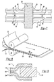
- FIG. 1 of the drawings there is shown a schematic diagram illustrating the various manufacturing steps of the present invention.
- An apparatus 10 is used to manufacture a circuit assembly.
- Apparatus 10 includes feed stock of coiled metal layers 12,14.
- the metal layers 12, 14 may be either a single layer of metal that may be formed into conductor traces, or more preferred, the metal layers 12, 14 are each two or more metal layers that may be partially etched to form a densely packed circuit assembly. Most preferred are tri-metal laminates made of two outer layers and an intermediate support layer.
- An example of this construction is illustrated in commonly assigned US patent application titled: "A multi-layer printed circuit board and method of making same", serial number 08/786494, filed 1/21/1997, and incorporated herein by reference.
- Circuitry patterns are applied to the metal layers 12, 14 by either an additive or subtractive photodefinition method.
- the inner metal layer of the tri-metal laminate is more susceptible to etching. This inner layer is in metal layers 12, 14 and is subsequently removed after lamination. This inner layer serves to strengthen the metal layers 12, 14 to withstand a calendaring process that will be described is greater detail below.
- Suitable tri-metal laminates are made from Cu/Al/Cu sandwich structures. Other combinations of metals are also suitable for use in this invention including Cu/Ni/Cu and Ni/Cu/Ni.
- the tri-metal layers generally have dimensions of 50 ⁇ m/150 ⁇ m/50 ⁇ m.
- the metal layers 12, 14 are bonded to a film carrier 16.
- the film carrier 16 may be either a dielectric material such as plastic or alternatively, film carrier 16 may be a metal foil that is coated with a dielectric coating. Polymer and insulated metal matrix composite or other solid materials with non-electrically conducting surfaces may be used. Illustrated in figure 1 is a film carrier 16 made from a thermoplastic film. Suitable thermoplastic films include poly (ethylene terapthlate (PET or MylarTM), and poly (etherimide) (UltemTM) having a thickness ranging from 75-500 ⁇ m.
- PET or MylarTM poly (ethylene terapthlate
- UltemTM poly (etherimide) having a thickness ranging from 75-500 ⁇ m.
- the film carrier 16 is placed between the metal layers 12, 14 and passed between calendaring rollers 18, 20. The rollers 18, 20 are heated and soften the film carrier 16 between the metal layers 12, 14.
- the etching bath 22 removes one or more of the tri-metal laminate layers. Generally, the etching bath removes an inner metal layer of aluminium or nickel to expose air bridges in the metal layers 12, 14. When the metal layers 12, 14 are made from a single layer of metal, the etching bath 22 removes excess metal to leave conductor traces for the circuit assembly.
- the composition of the etching bath 22 is selected to remove the metal used on the metal layers 12, 14 as are commonly used in electronic circuit manufacturing. After the laminate is etched, it is washed and dried and rolled into coils 24 for storage or transport. Alternatively, the laminate may be cut into sheets and fabricated into electronic circuits.
- the invention thus described provides a continuous method of manufacturing a circuit assembly from separate metal layers and a separate carrier layer.
- the lamination, etching and drying stages all may occur without removing the laminate from the apparatus 10.
- the invention as thus described uses an intermediate thermoplastic film carrier.
- Other types of materials are also suitable. Illustrated in figure 2 is an apparatus 10' having a film carrier 16' that is made from an extruded sheet of poly (etherimide) material.
- An adhesive 26 is applied to film 16'.
- the adhesive 26 adheres the film 16' to the metal layers 12, 14 and may eliminate the need to heat the rollers 18, 20.
- the rollers 18, 20 compress the film 16' between the metal layers 12, 14 to form a laminate. The remainder of the process is the same as that described above.
- the carrier 16" is made from a metal foil such as stainless steel or epoxy-coated mild steel having a thickness of about 150 microns.
- the metal may act as a ground plane for the circuit assembly and provide the resultant electronic device with EMI and RMI shielding.
- the metal foil When using a metal foil as a carrier, the metal foil must be coated with a dielectrical material to provide electrical insulation.
- the metal foil may be pre-coated or the apparatus 10" may also include roller coaters 28, 30 to apply a dielectric coating to the carrier 16". Suitable dielectric coatings include generic epoxy, polyurethane or any other electrically insulating polymer material able to withstand subsequent processing and environmental conditions.
- the dielectric coating may be applied using roll coaters 28, 30. Suitable roll coating applicators include direct and reverse coaters. When the dielectric coating applied is a thermoplastic adhesive, no further materials are needed to adhere the carrier 16" to the metal layers 12, 14. The rollers 18, 20 laminate the circuit assembly together.
- the circuit assembly 32 comprises two etched tri-metal layers 12, 14.
- the layers 12, 14 are made from two copper layers 34 and an inner aluminium layer 36. This construction is useful for making tightly spaced circuit assemblies having air bridges 38.
- the metal layers 12, 14 are bonded to the carrier 16".
- the carrier 16" includes a metal foil layer 40 and a dielectric coating 42.
- the dielectric coating 42 bonds the foil layer 40 to the metal layers 12, 14.
- a similar construction is used for carriers made of thermoplastic film or adhesive.
- the metal layers 12, 14 may be interconnected. Different types of interconnections are possible including edge connectors that wrap around the edge of the circuit assembly 32. More preferred are interconnections through the carrier 16, 16' and 16".
- FIG. 5 The interior electrical connection between the circuitry on both sides of the insulating carrier is brought about by a number of methods including, but not limited to, conventional circuit hole drilling and plated thru-hole processing and its variations, hole drilling and riveting.
- Figures 5 - 7 show the plated thru hole, rivet/clip, and soldered pin variations respectively, all involving a drilled or punched hole entirely through the bonded multi-layer chemically milled circuit following final etching.
- Figure 5 illustrates the plated-thru hole approach in which a passage 44 is drilled through the entire multi-layer structure and subsequently activated, and plated with a conductive material 46 to form a conductive path between all conductive layers of the circuit assembly 32.
- FIG. 6 illustrates the approach involving a mechanically-formed hole followed by inserting an expandable riveted 48 between outer conductive layers. This rivet 48 can be metallurgically or adhesively bonded as an additional step.
- Figure 7 shows the interconnection variation in which a mechanically drilled hole is filled with a pin 50 which is then soldered 52 to the outer conductive surfaces of the circuit assembly 32.
- An alternate interconnection involves soldering, welding or joining lateral extensions of adjacent trimetal from both sides of the dielectric carrier film with an electrically conductive material.
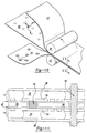
- This variation is represented in figures 8 and 9.
- the relevant region of the multi-layer flexible chemically-milled circuit from Figure 8 is expanded in figure 9.
- Conductive overhang tabs 54 protruding from either or both edges of the continuously processed flexible chemically-milled circuit web are juxtaposed and conductively joined 56 through any number of known processes including, but not limited to, seam welding, soldering, brazing, or the use of interposing conductive materials including metal-filled polymers.
- the central dielectric carrier 58 is perforated 60 and aligned between adjacent areas of both sides of the partially etched chemically-milled circuit structures as shown in figure 11.
- the actual electrical interconnection is accomplished through direct contact of the layers 12, 14 with a conductive material 62.
- the perforated areas 60 align with the conductive material 62.
- the conductive material 62 includes solder, conductive adhesive or a metal pad. Alternatively, the conductive material 62 may be added after the lamination process.
- perforated carrier 58 requires precise alignment of all layers during the bonding process. This alignment is accomplished by numerous methods including the use of index or ratchet holes corresponding to feed gears on the hot roll lamination station. Alternative machine vision and mechanical alignment methods may be used.
- a perforated dielectrically coated metal carrier 58 may be aligned and laminated as described above.
- the sites of the perforations 60 in the flexible carrier 58 correspond to sites of eventual electrical interconnection metal layers 12, 14.
- holes are formed through the layers 12, 14 drilling, punching or other process at locations corresponding to the perforations 60. The diameter of these holes is less than the size of the perforation 60 to prevent circuit shorting.
- Pins 64 are placed and soldered in the drilled holes to complete the connection as shown in figure 11. These pins 64 may also be insulated to provide added protection from shorting to the metal carrier 58.
- the carrier 16"' includes a series of regularly spaced rigid panels 66 that extend transversely to the carrier 16"' as shown in figure 12.
- the rigid panels 66 provide a rigid backing for the tri-metal layers 12, 14.
- the rigid panels 66 may be used in high vibration applications or when the size or number of airbridges on the circuit assembly 32 require more support than is available with a flexible carrier.
- the rigid panels 66 are made from plastic or metal plaque attached to a continuous carrier layer.
- the carrier 16"' may still be rolled into coils and processed using the continuous machining apparatus described because it may flex between the rigid panels. After the tri-metal layers 12, 14 are attached and etched, the carrier 16"' and the layers 12, 14 are cut by blades 68 into boards 70.
- the methods taught above may be adapted to form a circuit assembly having one side made from a tri-metal layer and a second side made from a flexible or rigid circuit layer.
- Figures 13-14 illustrate attaching a tri-metal layer 12 to a two-sided flex circuit 15.
- the flex circuit 15 is constructed from a flexible film carrier 16"" having conductive traces 72 on both surfaces of the carrier 16"".
- the tri-metal layer 12 is aligned atop the flex circuit 15 and bonded thereto using an adhesive sheet 26'.
- the bonded circuit assembly 32' is processed in an etching bath as described above.
- a soldering pin 64 electrically connects the tri-metal layer 12 to the flex circuit 15.
- the flex circuit 15 may also be replaced with a wide variety of circuits including single, double and multi-layer flexible circuits. These circuits may result from either additive, semi-additive, or subtractive processing and may be composed of numerous electrical conductive materials such as copper or nickel and may be separated by numerous electrically insulative materials such as polyester or polyimide polymers.
- the invention has been described as a method of attaching two etched tri-metal layers.
- Single or double metal layers may be used to form double sided circuit assemblies.
- Single sided circuit assemblies with a carrier film may also be fabricated using the method and apparatus described.
- the invention has been described as a continuous method of manufacturing circuit assemblies using flexible coiled stock.
- Glass reinforced printed wiring boards may be used in a continuous process if they are made sufficiently flexible to be processed using the equipment described above. It is also possible to use the same methods taught herein to manufacture the circuit assemblies in a batch process where individual sheets of the various layers are bonded together in a vertical or horizontal press. This batch process may utilise rigid glass reinforce printed wiring boards because they need not bend in the roll presses.
Landscapes
- Engineering & Computer Science (AREA)
- Manufacturing & Machinery (AREA)
- Microelectronics & Electronic Packaging (AREA)
- Laminated Bodies (AREA)
- Production Of Multi-Layered Print Wiring Board (AREA)
- Parts Printed On Printed Circuit Boards (AREA)
- Manufacturing Of Printed Wiring (AREA)
Applications Claiming Priority (2)
| Application Number | Priority Date | Filing Date | Title |
|---|---|---|---|
| US09/006,213 US5976391A (en) | 1998-01-13 | 1998-01-13 | Continuous Flexible chemically-milled circuit assembly with multiple conductor layers and method of making same |
| US6213 | 1998-01-13 |
Publications (2)
| Publication Number | Publication Date |
|---|---|
| EP0929208A2 true EP0929208A2 (fr) | 1999-07-14 |
| EP0929208A3 EP0929208A3 (fr) | 2003-02-12 |
Family
ID=21719820
Family Applications (1)
| Application Number | Title | Priority Date | Filing Date |
|---|---|---|---|
| EP99300207A Withdrawn EP0929208A3 (fr) | 1998-01-13 | 1999-01-12 | Assemblage de circuits flexibles chimiquement gravés ayant des couches conductrices multiples et son procédé de fabrication |
Country Status (2)
| Country | Link |
|---|---|
| US (1) | US5976391A (fr) |
| EP (1) | EP0929208A3 (fr) |
Cited By (6)
| Publication number | Priority date | Publication date | Assignee | Title |
|---|---|---|---|---|
| WO2001050824A1 (fr) * | 1999-12-31 | 2001-07-12 | Lear Automotive (Eeds) Spain, S.L. | Procede de fabrication de plaquettes de circuits imprimes |
| EP1187519A3 (fr) * | 2000-09-06 | 2003-01-15 | Visteon Global Technologies, Inc. | Panneau à circuit électrique et son procédé de fabrication |
| EP1187520A3 (fr) * | 2000-09-06 | 2003-01-15 | Visteon Global Technologies, Inc. | Panneau à circuit électrique et son procédé de fabrication |
| CN104853545A (zh) * | 2014-02-13 | 2015-08-19 | 日本梅克特隆株式会社 | 柔性印刷电路板的制造方法及其中间产物 |
| CN113015333A (zh) * | 2021-01-27 | 2021-06-22 | 许泽楠 | 一种光电产品柔性电路板加工用夹持装置 |
| WO2021224548A1 (fr) * | 2020-05-04 | 2021-11-11 | Teknologian Tutkimuskeskus Vtt Oy | Procédé de fabrication d'un appareil électronique et appareil électronique |
Families Citing this family (23)
| Publication number | Priority date | Publication date | Assignee | Title |
|---|---|---|---|---|
| US6817532B2 (en) * | 1992-02-12 | 2004-11-16 | Lenscard U.S., Llc | Wallet card with built-in light |
| US6528736B1 (en) * | 1997-01-21 | 2003-03-04 | Visteon Global Technologies, Inc. | Multi-layer printed circuit board and method of making same |
| JP3901798B2 (ja) * | 1997-06-12 | 2007-04-04 | 大日本印刷株式会社 | プリント配線板の製造装置 |
| US6475703B2 (en) * | 1998-12-01 | 2002-11-05 | Visteon Global Technologies, Inc. | Method for constructing multilayer circuit boards having air bridges |
| US6365057B1 (en) | 1999-11-01 | 2002-04-02 | Bmc Industries, Inc. | Circuit manufacturing using etched tri-metal media |
| US6468439B1 (en) | 1999-11-01 | 2002-10-22 | Bmc Industries, Inc. | Etching of metallic composite articles |
| US6409930B1 (en) | 1999-11-01 | 2002-06-25 | Bmc Industries, Inc. | Lamination of circuit sub-elements while assuring registration |
| DE10016715C1 (de) * | 2000-04-04 | 2001-09-06 | Infineon Technologies Ag | Herstellungsverfahren für laminierte Chipkarten |
| DE10048680C1 (de) * | 2000-09-30 | 2002-04-25 | Oechsler Ag | Elektrische Stromschiene,deren Verwendung und Verfahren zu ihrer Herstellung |
| US6454878B1 (en) * | 2000-11-01 | 2002-09-24 | Visteon Global Technologies, Inc. | Cladded material construction for etched-tri-metal circuits |
| DE10120269C1 (de) * | 2001-04-25 | 2002-07-25 | Muehlbauer Ag | Verfahren zum Verbinden von Mikrochips mit auf einem Trägerband angeordneten Antennen zum Herstellen eines Transponders |
| US6506062B1 (en) | 2001-08-01 | 2003-01-14 | Visteon Global Technologies, Inc. | Circuit board having an integrated circuit board connector and method of making the same |
| US6665191B2 (en) * | 2001-09-10 | 2003-12-16 | Cardiac Pacemakers, Inc. | Multi-folded printed wiring construction for an implantable medical device |
| TWI312166B (en) * | 2001-09-28 | 2009-07-11 | Toppan Printing Co Ltd | Multi-layer circuit board, integrated circuit package, and manufacturing method for multi-layer circuit board |
| US6701614B2 (en) * | 2002-02-15 | 2004-03-09 | Advanced Semiconductor Engineering Inc. | Method for making a build-up package of a semiconductor |
| US7293355B2 (en) * | 2005-04-21 | 2007-11-13 | Endicott Interconnect Technologies, Inc. | Apparatus and method for making circuitized substrates in a continuous manner |
| DE102009015742B4 (de) * | 2009-03-31 | 2013-09-05 | Fraunhofer-Gesellschaft zur Förderung der angewandten Forschung e.V. | Elektrisch funktionales Mehrschichtfoliensystem und Verfahren zum Herstellen desselben |
| GB2498994B (en) * | 2012-02-02 | 2014-03-19 | Trackwise Designs Ltd | Method of making a flexible circuit |
| EP2947685A4 (fr) * | 2013-11-22 | 2016-04-27 | Silicone Valley Co Ltd | Plage de test de semi-conducteur ayant des feuillets métalliques empilés et son procédé de fabrication |
| WO2015177684A1 (fr) * | 2014-05-22 | 2015-11-26 | Sabic Global Technologies B.V. | Ensembles circuit et procédé pour les fabriquer |
| CN106413238B (zh) * | 2016-06-03 | 2019-09-10 | 武汉华星光电技术有限公司 | 柔性电路板的制作方法 |
| US10278283B1 (en) * | 2017-12-14 | 2019-04-30 | Wen Yao Chang | Method for forming a circuit board with a substrate made of silicon |
| US11197401B2 (en) * | 2019-01-22 | 2021-12-07 | Honeywell Federal Manufacturing & Technologies, Llc | System and method for large-scale PCB production including continuous selective adhesion |
Family Cites Families (37)
| Publication number | Priority date | Publication date | Assignee | Title |
|---|---|---|---|---|
| US2926340A (en) * | 1956-01-26 | 1960-02-23 | Sperry Rand Corp | Edge connectors |
| US3334395A (en) * | 1962-11-26 | 1967-08-08 | Northrop Corp | Method of making a metal printed circuit board |
| CA757597A (en) * | 1963-12-30 | 1967-04-25 | International Business Machines Corporation | Method for making printed circuits |
| US3448516A (en) * | 1966-02-14 | 1969-06-10 | Norman R Buck | Method of preparing printed wiring |
| FR1517061A (fr) * | 1967-02-02 | 1968-03-15 | Constr Telephoniques | Perfectionnements aux circuits imprimés |
| BE661207A (fr) * | 1968-05-13 | 1965-07-16 | ||
| US3772776A (en) * | 1969-12-03 | 1973-11-20 | Thomas & Betts Corp | Method of interconnecting memory plane boards |
| US3728178A (en) * | 1970-07-30 | 1973-04-17 | Olin Corp | Method of producing flexible copper laminate for printed circuits |
| US3728177A (en) * | 1970-07-30 | 1973-04-17 | Olin Corp | Method of producing a flexible laminate copper circuit |
| JPS5146904B2 (fr) * | 1971-09-30 | 1976-12-11 | ||
| JPS5545382B2 (fr) * | 1972-10-04 | 1980-11-18 | ||
| US4052787A (en) * | 1975-12-18 | 1977-10-11 | Rockwell International Corporation | Method of fabricating a beam lead flexible circuit |
| US4395459A (en) * | 1978-07-11 | 1983-07-26 | Herschdorfer C George | Reinforced laminates produced from crosslinkable thermoplastic olefin polymer material |
| US4447519A (en) * | 1981-12-16 | 1984-05-08 | Nathan Pritikin | Solid photoresist and method of making photoresist |
| EP0089387A1 (fr) * | 1982-03-19 | 1983-09-28 | Uop Inc. | Fabrication de produits stratifiés revêtus de cuivre |
| US4404059A (en) * | 1982-05-26 | 1983-09-13 | Livshits Vladimir I | Process for manufacturing panels to be used in microelectronic systems |
| US4480288A (en) * | 1982-12-27 | 1984-10-30 | International Business Machines Corporation | Multi-layer flexible film module |
| US4517051A (en) * | 1982-12-27 | 1985-05-14 | Ibm Corporation | Multi-layer flexible film module |
| US4517050A (en) * | 1983-12-05 | 1985-05-14 | E. I. Du Pont De Nemours And Company | Process for forming conductive through-holes through a dielectric layer |
| US4584767A (en) * | 1984-07-16 | 1986-04-29 | Gregory Vernon C | In-mold process for fabrication of molded plastic printed circuit boards |
| US4679122A (en) * | 1984-10-09 | 1987-07-07 | General Electric Company | Metal core printed circuit board |
| US5047114A (en) * | 1984-11-02 | 1991-09-10 | Amp-Akzo Corporation | Process for the production of metal clad thermoplastic base materials and printed circuits on thermoplastic base materials |
| US4735676A (en) * | 1986-01-14 | 1988-04-05 | Asahi Chemical Research Laboratory Co., Ltd. | Method for forming electric circuits on a base board |
| US4659425A (en) * | 1986-02-03 | 1987-04-21 | Ibm Corporation | Continuous process for the manufacture of printed circuit boards |
| JPS63229897A (ja) * | 1987-03-19 | 1988-09-26 | 古河電気工業株式会社 | リジツド型多層プリント回路板の製造方法 |
| JPH0735106B2 (ja) * | 1988-11-15 | 1995-04-19 | 信越化学工業株式会社 | ポリイミドフィルム系フレキシブル印刷回路用基板の製造方法 |
| JPH0371839A (ja) * | 1989-08-11 | 1991-03-27 | Matsushita Electric Works Ltd | 積層板の製造方法 |
| US4997517A (en) * | 1990-01-09 | 1991-03-05 | Olin Corporation | Multi-metal layer interconnect tape for tape automated bonding |
| JP2874329B2 (ja) * | 1990-11-05 | 1999-03-24 | 日本電気株式会社 | 多層印刷配線板の製造方法 |
| US5118385A (en) * | 1991-05-28 | 1992-06-02 | Microelectronics And Computer Technology Corporation | Multilayer electrical interconnect fabrication with few process steps |
| FR2678468A1 (fr) * | 1991-06-26 | 1992-12-31 | Set Services Tech | Procede d'isolation d'un circuit electrique flexible, dispositif pour la mise en óoeuvre dudit procede et produits ainsi obtenus. |
| JP2658661B2 (ja) * | 1991-09-18 | 1997-09-30 | 日本電気株式会社 | 多層印刷配線板の製造方法 |
| US5433819A (en) * | 1993-05-26 | 1995-07-18 | Pressac, Inc. | Method of making circuit boards |
| JPH07254771A (ja) * | 1994-03-14 | 1995-10-03 | Yaskawa Electric Corp | 大電流用プリント基板の製造方法 |
| JP3593234B2 (ja) * | 1996-04-23 | 2004-11-24 | 日立電線株式会社 | 半導体装置用両面配線テープキャリアの製造方法 |
| US5819401A (en) * | 1996-06-06 | 1998-10-13 | Texas Instruments Incorporated | Metal constrained circuit board side to side interconnection technique |
| US5679444A (en) * | 1996-07-15 | 1997-10-21 | International Business Machines Corporation | Method for producing multi-layer circuit board and resulting article of manufacture |
-
1998
- 1998-01-13 US US09/006,213 patent/US5976391A/en not_active Expired - Fee Related
-
1999
- 1999-01-12 EP EP99300207A patent/EP0929208A3/fr not_active Withdrawn
Cited By (9)
| Publication number | Priority date | Publication date | Assignee | Title |
|---|---|---|---|---|
| WO2001050824A1 (fr) * | 1999-12-31 | 2001-07-12 | Lear Automotive (Eeds) Spain, S.L. | Procede de fabrication de plaquettes de circuits imprimes |
| US6952871B1 (en) | 1999-12-31 | 2005-10-11 | Lear Automotive (Eeds) Spain, S.L. | Method for manufacturing printed circuit boards |
| EP1187519A3 (fr) * | 2000-09-06 | 2003-01-15 | Visteon Global Technologies, Inc. | Panneau à circuit électrique et son procédé de fabrication |
| EP1187520A3 (fr) * | 2000-09-06 | 2003-01-15 | Visteon Global Technologies, Inc. | Panneau à circuit électrique et son procédé de fabrication |
| CN104853545A (zh) * | 2014-02-13 | 2015-08-19 | 日本梅克特隆株式会社 | 柔性印刷电路板的制造方法及其中间产物 |
| CN104853545B (zh) * | 2014-02-13 | 2019-08-27 | 日本梅克特隆株式会社 | 柔性印刷电路板的制造方法及其中间产物 |
| WO2021224548A1 (fr) * | 2020-05-04 | 2021-11-11 | Teknologian Tutkimuskeskus Vtt Oy | Procédé de fabrication d'un appareil électronique et appareil électronique |
| CN113015333A (zh) * | 2021-01-27 | 2021-06-22 | 许泽楠 | 一种光电产品柔性电路板加工用夹持装置 |
| CN113015333B (zh) * | 2021-01-27 | 2022-04-15 | 达翔技术(恩施)有限公司 | 一种光电产品柔性电路板加工用夹持装置 |
Also Published As
| Publication number | Publication date |
|---|---|
| US5976391A (en) | 1999-11-02 |
| EP0929208A3 (fr) | 2003-02-12 |
Similar Documents
| Publication | Publication Date | Title |
|---|---|---|
| US5976391A (en) | Continuous Flexible chemically-milled circuit assembly with multiple conductor layers and method of making same | |
| KR100854614B1 (ko) | 플렉스리지드 배선판과 그 제조 방법 | |
| EP0620701B1 (fr) | Dispositifs de circuit et leur procédé de fabrication | |
| US5004639A (en) | Rigid flex printed circuit configuration | |
| EP0568313A2 (fr) | Procédé de production d'une plaque à circuit imprimé multicouche | |
| EP1601053A1 (fr) | Circuit imprimé et disposition de connection | |
| US5709805A (en) | Method for producing multi-layer circuit board and resulting article of manufacture | |
| EP1404166A1 (fr) | Carte a circuits imprimes multicouche souple et procede de fabrication | |
| JPS6227558B2 (fr) | ||
| JP3226959B2 (ja) | 多層フレキシブルプリント基板の製法 | |
| EP1272019B1 (fr) | Carte imprimee, carte imprimee multicouche et procede de fabrication | |
| EP0782154A1 (fr) | Transformateur plat | |
| WO2004017689A1 (fr) | Plaquette a circuit imprime multicouche et son procede de production | |
| US8076589B2 (en) | Multilayer wiring board and its manufacturing method | |
| JP3167840B2 (ja) | 印刷配線板および印刷配線板の製造方法 | |
| JPH08153971A (ja) | 多層プリント配線基板及びその製造方法 | |
| JPH04336486A (ja) | プリント配線板 | |
| JPH05243741A (ja) | 多層フレキシブルプリント配線板 | |
| JP3155565B2 (ja) | プリント配線板の製造方法 | |
| US20080005896A1 (en) | Method for fabricating multi-layered flexible printed circuit board without via holes | |
| JP3179572B2 (ja) | 多層プリント配線板およびその製造方法 | |
| JPH05315758A (ja) | 多層フレキシブル回路基板およびその製法 | |
| JP2811995B2 (ja) | スルーホールプリント配線基板の製造方法 | |
| JPH05259600A (ja) | 配線板およびその製造法 | |
| JP2000133943A (ja) | 多層基板の製造方法 |
Legal Events
| Date | Code | Title | Description |
|---|---|---|---|
| PUAI | Public reference made under article 153(3) epc to a published international application that has entered the european phase |
Free format text: ORIGINAL CODE: 0009012 |
|
| AK | Designated contracting states |
Kind code of ref document: A2 Designated state(s): AT BE CH CY DE DK ES FI FR GB GR IE IT LI LU MC NL PT SE |
|
| AX | Request for extension of the european patent |
Free format text: AL;LT;LV;MK;RO;SI |
|
| PUAL | Search report despatched |
Free format text: ORIGINAL CODE: 0009013 |
|
| AK | Designated contracting states |
Designated state(s): AT BE CH CY DE DK ES FI FR GB GR IE IT LI LU MC NL PT SE |
|
| AX | Request for extension of the european patent |
Extension state: AL LT LV MK RO SI |
|
| 17P | Request for examination filed |
Effective date: 20030716 |
|
| AKX | Designation fees paid |
Designated state(s): DE FR GB |
|
| STAA | Information on the status of an ep patent application or granted ep patent |
Free format text: STATUS: THE APPLICATION HAS BEEN WITHDRAWN |
|
| 18W | Application withdrawn |
Effective date: 20031116 |