EP0931437B1 - Procede de production de series d'impulsions de tension pour faire fonctionner des lampes a decharge a barriere dielectrique, et circuit associe - Google Patents
Procede de production de series d'impulsions de tension pour faire fonctionner des lampes a decharge a barriere dielectrique, et circuit associe Download PDFInfo
- Publication number
- EP0931437B1 EP0931437B1 EP98944997A EP98944997A EP0931437B1 EP 0931437 B1 EP0931437 B1 EP 0931437B1 EP 98944997 A EP98944997 A EP 98944997A EP 98944997 A EP98944997 A EP 98944997A EP 0931437 B1 EP0931437 B1 EP 0931437B1
- Authority
- EP
- European Patent Office
- Prior art keywords
- voltage
- sequence
- voltage pulses
- pulse
- sequences
- Prior art date
- Legal status (The legal status is an assumption and is not a legal conclusion. Google has not performed a legal analysis and makes no representation as to the accuracy of the status listed.)
- Expired - Lifetime
Links
- 238000000034 method Methods 0.000 title claims description 17
- 230000004888 barrier function Effects 0.000 title description 2
- 230000000630 rising effect Effects 0.000 claims abstract description 9
- 230000001360 synchronised effect Effects 0.000 claims abstract description 4
- 238000004519 manufacturing process Methods 0.000 claims abstract 2
- 239000003989 dielectric material Substances 0.000 claims 2
- 239000000203 mixture Substances 0.000 claims 2
- 239000012811 non-conductive material Substances 0.000 claims 2
- 230000002123 temporal effect Effects 0.000 description 10
- 230000005855 radiation Effects 0.000 description 6
- 238000004804 winding Methods 0.000 description 3
- 239000003990 capacitor Substances 0.000 description 2
- 230000001419 dependent effect Effects 0.000 description 2
- 230000008878 coupling Effects 0.000 description 1
- 238000010168 coupling process Methods 0.000 description 1
- 238000005859 coupling reaction Methods 0.000 description 1
- 238000010586 diagram Methods 0.000 description 1
- 230000000694 effects Effects 0.000 description 1
- 230000005670 electromagnetic radiation Effects 0.000 description 1
- 238000005516 engineering process Methods 0.000 description 1
- 239000011521 glass Substances 0.000 description 1
- 239000007924 injection Substances 0.000 description 1
- 238000002347 injection Methods 0.000 description 1
- 230000002093 peripheral effect Effects 0.000 description 1
- 238000007650 screen-printing Methods 0.000 description 1
- 229910052709 silver Inorganic materials 0.000 description 1
- 239000004332 silver Substances 0.000 description 1
- 229910000679 solder Inorganic materials 0.000 description 1
- 230000003595 spectral effect Effects 0.000 description 1
- 230000036962 time dependent Effects 0.000 description 1
Images


Classifications
-
- H—ELECTRICITY
- H05—ELECTRIC TECHNIQUES NOT OTHERWISE PROVIDED FOR
- H05B—ELECTRIC HEATING; ELECTRIC LIGHT SOURCES NOT OTHERWISE PROVIDED FOR; CIRCUIT ARRANGEMENTS FOR ELECTRIC LIGHT SOURCES, IN GENERAL
- H05B41/00—Circuit arrangements or apparatus for igniting or operating discharge lamps
- H05B41/14—Circuit arrangements
- H05B41/26—Circuit arrangements in which the lamp is fed by power derived from DC by means of a converter, e.g. by high-voltage DC
- H05B41/28—Circuit arrangements in which the lamp is fed by power derived from DC by means of a converter, e.g. by high-voltage DC using static converters
- H05B41/2806—Circuit arrangements in which the lamp is fed by power derived from DC by means of a converter, e.g. by high-voltage DC using static converters with semiconductor devices and specially adapted for lamps without electrodes in the vessel, e.g. surface discharge lamps, electrodeless discharge lamps
-
- H—ELECTRICITY
- H05—ELECTRIC TECHNIQUES NOT OTHERWISE PROVIDED FOR
- H05B—ELECTRIC HEATING; ELECTRIC LIGHT SOURCES NOT OTHERWISE PROVIDED FOR; CIRCUIT ARRANGEMENTS FOR ELECTRIC LIGHT SOURCES, IN GENERAL
- H05B41/00—Circuit arrangements or apparatus for igniting or operating discharge lamps
- H05B41/14—Circuit arrangements
- H05B41/30—Circuit arrangements in which the lamp is fed by pulses, e.g. flash lamp
-
- Y—GENERAL TAGGING OF NEW TECHNOLOGICAL DEVELOPMENTS; GENERAL TAGGING OF CROSS-SECTIONAL TECHNOLOGIES SPANNING OVER SEVERAL SECTIONS OF THE IPC; TECHNICAL SUBJECTS COVERED BY FORMER USPC CROSS-REFERENCE ART COLLECTIONS [XRACs] AND DIGESTS
- Y02—TECHNOLOGIES OR APPLICATIONS FOR MITIGATION OR ADAPTATION AGAINST CLIMATE CHANGE
- Y02B—CLIMATE CHANGE MITIGATION TECHNOLOGIES RELATED TO BUILDINGS, e.g. HOUSING, HOUSE APPLIANCES OR RELATED END-USER APPLICATIONS
- Y02B20/00—Energy efficient lighting technologies, e.g. halogen lamps or gas discharge lamps
Definitions
- the invention relates to a method for generating pulse voltage sequences for the operation of discharge lamps by means of pulsed, dielectric disabled discharge according to the preamble of claim 1.
- the invention relates to an electrical circuit arrangement for generating of pulse voltage sequences according to this method.
- the concerns Invention also a lighting system with this circuit arrangement.
- discharge lamp Such radiation sources are also included under the term “discharge lamp” to understand that in addition to electromagnetic radiation in the visible spectral range, i.e. light, also or even predominantly radiation in UV or Emit VUV area.
- the pulse voltage sequence can be both unipolar and bipolar and is used to operate discharge lamps or emitters at least the electrodes of one polarity are dielectrically impeded, as described for example in WO 94/23442.
- This mode of operation uses a basically unlimited sequence of voltage pulses, during which primarily electrical active power is injected and which are separated from each other by dead times.
- Crucial for that Efficiency of the generation of useful radiation are essentially the pulse shape, in particular steep increases, as well as the duration of the pulse or dead times.
- the required peak values of the voltage pulses are - depending on, among other things, the stroke distance, the type and the pressure of the filling gas and the type and thickness of the dielectric - typically one up to several kilovolts.
- Such a circuit arrangement for generating pulse voltage sequences with exactly one pulse circuit is already known from the document DE 195 48 003 A1.
- This pulse circuit essentially consists of a capacitor, a transistor and a pulse transformer. During the conducting phase of the transistor, the energy stored in the capacitor is transferred to the pulse transformer.
- the pulse transformer transforms the pulse voltage to the required peak values, but this has some disadvantages.
- the pulse transformer has to be designed for the peak value of the pulse voltage sequence and is therefore relatively large and expensive.
- the pulse load of the pulse transformer is relatively large and the also relatively large winding capacities affect the pulse shape.
- Another disadvantage is that the full peak value of the pulse voltage sequence occurs on the leads of the secondary winding of the pulse transformer. Due to the ubiquitous stray capacitances to the environment resulting from relatively high interference, so called EMI (E lectro m agnetic nterference I).
- Another object of the present invention is a circuit arrangement to provide for performing this procedure. This task is characterized by the features of the independent on the circuit arrangement Claim solved. Find other particularly advantageous features themselves in the dependent claims.
- the basic idea of the invention is the pulse voltage sequence to be composed of two partial voltage sequences such that the peak values each partial voltage sequence are smaller than the peak values of the resulting ones Pulse voltage sequence, for example, only half as large. This has the advantage that correspondingly when generating the partial voltage sequences lower EMI arise. It also contains one of the two partial voltage sequences positive rising edges with respect to a reference potential and the other partial voltage sequence contains with respect to this reference potential negative rising edges. The one of the two partial voltage sequences is preferably the inverse of the others with respect to the reference potential Partial voltage sequence. Ideally, they compensate for each other EMI generated partial voltage sequences completely, at least locally.
- WO 93/23975 describes a circuit arrangement for suppressing known from EMI for electrodeless discharge lamps with a symmetrical Filter arrangement consisting of two individual filters. Both single filters have a common reference potential and the output signals of the both filters are of the same height and opposite phase.
- this basic idea is implemented in the following method.
- the two partial sequences are superimposed in such a way that a sequence of differences arises. If necessary the two partial sequences are synchronized with one another in such a way that the peak values the difference sequence is greater than the peak values of each of the two individual partial sequences of voltage pulses.
- the individual impulses of the partial sequences can be both unipolar and bipolar.
- the term "bipolar pulse” means that within such Impulse the time-dependent voltage one or more times the sign changes. This results in accordance with the above procedure finally unipolar or bipolar differences. It is crucial only that the corresponding impulses of the two partial sequences are related of the common reference potential rising edges with mutually opposite Have slopes. In the bipolar case, the electrodes take over depending on the phase of the pulse both the role of the anode and the Cathode.
- one partial sequence of voltage pulses by inverting the other Partial sequence formed by voltage pulses.
- the synchronization takes place in such a way that the peaks of the sequence of differences are the sum of the peaks of the partial sequences are.
- At least one additional method step one of the two partial sequences of voltage pulses and / or the sequence of differences an offset DC voltage is additively superimposed, the total offset DC voltage is chosen so that the discharge (s) after each Voltage pulse can go out and unwanted re-ignition between the individual voltage pulses is prevented.
- a relevant voltage component can be determined by the direct voltage provide. This has the advantage that the pulse circuits only on the rest Voltage component must be designed.
- the circuit arrangement according to the invention for generating pulse voltage sequences according to the method described above two pulse circuits connected in series, each with two output poles and one each Control input as well as a timer circuit that is connected to the control inputs of the two pulse circuits is connected.
- One of the two output poles of the first pulse circuit is of opposite polarity with the output pole of the second pulse circuit.
- the connection of the two mentioned Output poles sets the reference potential in relation to the two free output poles of the two pulse circles. This way lies between the between the two free output poles, the difference signal between the two a free output pole and the reference potential signals.
- the reference potential can, but does not necessarily have to be with the Circuit ground or connected to earth potential.
- the two pulse circles are, for example, each in accordance with the DE 195 48 003 A1 disclosed circuit constructed.
- the advantage over the state of the art here is that for a specifiable peak voltage required translation and consequently winding ratios of the two Transformers smaller, for example with a symmetrical design are only half the size of each. This results in a further advantage that steeper Edges of the voltage pulses and consequently a higher efficiency of the Useful radiation generation can be achieved.
- impulse circles will depend on the individual Align the required peak values with the electrodes. Relevant for the advantageous effect of the circuit is primarily that the two pulse circuits are suitable, a partial sequence of each other by pauses to deliver separate voltage pulses, the partial voltage sequences in each case Rising edges with opposite slopes included.
- the timer circuit controls the two pulse circuits in such a way that the two Partial voltage sequences are synchronized with each other.
- At least one of the two free connection poles is the Pulse circles with the pole of opposite polarity one Offset DC voltage source connected. In this way, the one Variant of the method explained offset DC voltage realized.
- FIG. 1 shows a schematic representation of the block diagram of the circuit arrangement according to the invention for generating pulse voltage sequences and a flat radiator.
- the circuit arrangement essentially consists of a first and a second pulse circuit 1, 2 and a timer 3.
- Each of the two pulse circuits each has a control input a; d and two output poles b, c; e, f on.
- the two pulse circuits 1, 2 each supply a partial voltage sequence U 1 and U 2 between their output poles b, c and e, f.
- Each of the two control inputs is connected to the timer 3.
- the timer 3 is used to synchronize the two pulse circuits 1; 2.
- the positive (+) output pole b of the first pulse circuit 1 and the negative (-) output pole f of the second pulse circuit 2 are connected to connections 4 and 5, respectively.
- the connections 4 and 5 are in turn connected to the flat radiator 8 via feed lines 6, 7.
- the respective free output poles c; e of the two pulse circuits 1, 2 are connected to one another and to earth potential, which serves as a reference potential.
- the two pulse circuits 1, 2 are connected in series and, during operation, a differential voltage sequence U 3 is generated between the positive (+) output pole b of the first pulse circuit 1 and the negative (-) output pole f of the second pulse circuit 2.
- the flat radiator 8 consists of a discharge vessel 9, strip-shaped Cathodes 10 and dielectric barrier, strip-shaped anodes 11.
- Das Discharge vessel 9 consists of a base plate 12 and a cover plate 13 and a frame 14, all of which have a rectangular base area.
- Base plate 12 and ceiling plate 13 are by means of glass solder with the frame connected gas-tight in such a way that the interior of the discharge vessel 9 is cuboid is trained.
- the base plate 12 is larger than the cover plate 13 such that the discharge vessel 9 has a peripheral free-standing edge having.
- the cathodes 10 and anodes 11 are alternating and parallel 6 mm apart on the inner wall the bottom plate 12 is arranged.
- the cathodes 10 and anodes 11 are on opposite ends extended and from the inside of the discharge vessel 9 on the base plate 12 out on both sides. On the cathode 10 and anode 11 go to the edge of the base plate 12, respectively into cathode-side 15 or anode-side 16 external power supply lines.
- the outer power supply lines 15, 16 are each by means of a short connecting piece 17, 18 connected to the feed lines 6, 7.
- the breakthrough in the ceiling tile 13 is only for illustration Purposes and gives a view of part of the anodes 11 and cathodes 10 free.
- the anodes 11 are completely with a glass layer 19 covered, the thickness of which is approximately 250 ⁇ m.
- the electrodes 10; 11 and external contacts 15; 16 are different sections of one realized on the cathode side and an anode side layer structure made of silver, that together using screen printing technology and subsequent baking are upset.
- the layer thickness is approx. 6 ⁇ m.
- applies
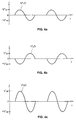
- FIGS. 3a and 3b ideally show two further partial voltage sequences U ' 1 (t) and U' 2 (t).
- an offset direct voltage of the amplitude U DC is additively superimposed on the voltage signal in FIG. 3b. This also results in an offset DC voltage of the amplitude U DC in the differential signal U ' 3 (t), ie
Landscapes
- Circuit Arrangements For Discharge Lamps (AREA)
- Discharge-Lamp Control Circuits And Pulse- Feed Circuits (AREA)
- Lasers (AREA)
Claims (10)
- Procédé de production de trains (U3(t) ; U'3(t) ; - U"3(t)) d'impulsions de tension pour faire fonctionner des lampes (8) à décharge au moyen de décharge(s) pulsée(s) à barrière diélectrique, comprenantcaractérisé par les stades suivants du procédéune enceinte (9) de décharge, au moins partiellement transparente, et fermée en étant emplie d'une atmosphère gazeuse ou ouverte en étant parcourue par un gaz ou par un mélange gazeux, l'enceinte étant en un matériau non conducteur de l'électricité, etdes électrodes d'une première et d'une deuxième polarités (10 et 11), au moins des électrodes (11) d'une polarité étant séparées de l'intérieur de l'enceinte de décharge par du matériau (9) diélectrique,mise à disposition d'un premier sous-train (U1(t) ; U'1(t) ; U"1(t)) d'impulsions de tension séparées les unes des autres par des intervalles et ayant des premières valeurs de crête (U1S ; U'1S ; U"1S) et des fronts de montée positifs par rapport à un potentiel de référence, le potentiel (o) de référence étant découplé des électrodes,mise à disposition d'un deuxième sous-train (U2(t) ; U'2(t) ; U"2(t)) d'impulsions de tension séparées les unes des autres par des intervalles et ayant des secondes valeurs (U2S ; U'2S ; U"2S) de crête et des fronts de montée négatifs par rapport au potentiel (o) de référence,application du premier sous-train (U1(t) ; U'1(t) ; U"1(t)) d'impulsions de tension aux électrodes (11) de la première polarité (+),application du deuxième sous-train (U2(t) ; U'2(t) ; U"2(t)) d'impulsions de tension à l'électrode (10) de la deuxième polarité (-),synchronisation des deux sous-trains (U1(t), U2(t) et U'1(t), U'2(t) et U"1(t), U"2(t)) d'impulsions de tension l'un avec l'autre, de façon à produire entre les électrodes (10, 11) de polarité opposée un train (U3(t) ; U'3(t) ; U"3(t)) différentiel d'impulsion de tension, les valeurs absolues des valeurs de crête (U3S ; U'3S ; U"3S) du train (U3(t) ; U'3(t) ; U"3(t)) différentiel étant plus grandes que les valeurs absolues des valeurs de crête (U1S, U2S ; U'1S, U'2S ; U"1S, U"2S) de chacun des deux sous-trains (U1(t), U2(t) et U'1(t), U'2(t) et U"1(t), U"2(t)) d'impulsions de tension.
- Procédé suivant la revendication 1, caractérisé en ce qu'il consiste à former le deuxième sous-train (U2(t) ; U'2(t) ; U"2(t)) d'impulsions de tension par l'inversion du premier sous-train (U1(t) ; U'1(t) ; U"1(t)) d'impulsions de tension et à effectuer la synchronisation de façon que les valeurs absolues des valeurs de crête (|U3S| ;|U'3S| ;|U"3S |) du train (U3(t) ; U'3(t) ; U"3(t)) différentiel représentent la somme des valeurs absolues des valeurs de crête (|U1S|, |U2S| ;|U'1S|, (|U'2S| ;|U"1S| ;|U"2S |) des deux sous-trains (U1(t), U2(t) et U'1(t), U'2(t) et U"1(t), U"2(t)).
- Procédé suivant l'une des revendications 1 ou 2, caractérisé en ce qu'il consiste à superposer, en tant que stade de procédé supplémentaire, à au moins l'un des deux sous-trains (U'2(t)) d'impulsions de tension et/ou du train différentiel, une tension (UDC) continue d'offset, toute la tension continue d'offset étant choisie délibérément au plus si haute que la (les) décharge(s) peut (peuvent) s'éteindre après chaque impulsion de tension et que tout réallumage peu souhaitable entre les impulsions de tension individuelles est empêché.
- Procédé suivant la revendication 3, caractérisé par un stade de procédé supplémentaire dans lequel, pendant les intervalles, la tension continue d'offset est mise au potentiel de référence commun.
- Circuit de production de train d'impulsions de tension selon le procédé suivant l'une des revendications 1 à 4 pour faire fonctionner des lampes (8) à décharge au moyen d'une décharge pulsée à barrière diélectrique comprenantun premier circuit (1) d'impulsions ayant deux pôles (b, c) de sortie et une entrée (a) de commande, ce circuit (1) d'impulsions étant apte à fournir un premier train (U1) d'impulsions de tension séparées les unes des autres par dès intervalles,un deuxième circuit (2) d'impulsions ayant deux pôles (e, f) de sortie et une entrée (d) de commande et ce circuit (2) d'impulsions étant apte à fournir un deuxième train (U2) d'impulsions de tension séparées les unes des autres par des intervalles, l'un des deux pôles (c) de sortie du premier circuit (1) d'impulsions étant relié au pôle (e) de sortie de polarité opposé du deuxième circuit (2) d'impulsions, grâce à quoi on peut prélever entre les pôles (b, f) libres de sortie des deux circuits (1, 2) d'impulsions un train (U3) différentiel d'impulsions de tension, qui correspond à la différence des deux trains (U1, U2) d'impulsions de tension rapportés au potentiel de référence,un circuit (3) d'horloge qui est relié aux entrées (a, d) de commande des deux circuits (1, 2) d'impulsion et qui les commande de façon que les deux trains (U1, U2) d'impulsions de tension soient synchronisés l'un avec l'autre, de sorte que les valeurs de crête du train (U3) différentiel soient plus grandes que les valeurs de crête des deux trains (U1, U2) individuels d'impulsions de tension.
- Circuit suivant la revendication 5, caractérisé en ce que la liaison du pôle (c, e) de sortie de polarité opposée est reliée entre les deux circuits (1, 2) d'impulsions à un potentiel de référence du circuit.
- Circuit suivant la revendication 6, caractérisé en ce que le potentiel de référence est au potentiel de la terre.
- Circuit suivant l'une des revendications 5 à 7, caractérisé en ce que le deuxième circuit d'impulsions comporte un circuit inverseur qui inverse le deuxième train d'impulsions de tension par rapport au premier train.
- Circuit suivant l'une des revendications 5 à 8, caractérisé par un circuit de tension continue supplémentaire, dont l'un des pôles est relié au pôle de sortie libre de polarité opposé du circuit d'impulsions.
- Système d'éclairage comprenantcaractérisé en ce que la source (1 à 3) d'impulsions de tension comporte un circuit suivant l'une ou plusieurs des revendications 5 à 9.une lampe (8) de décharge qui convient pour une décharge à barrière diélectrique, la lampe (8) de décharge comprenant ce qui suit :une enceinte (8) de décharge, au moins partiellement transparente et fermée en étant emplie d'une atmosphère gazeuse ou ouverte en étant traversée par un gaz ou un mélange gazeux, l'enceinte étant en matériau non conducteur de l'électricité, etdes électrodes (10, 11) au moins les électrodes (11) d'une polarité étant séparées de l'intérieur de l'enceinte (9) de décharge par du matériau (19) diélectrique,une source (1 à 3) d'impulsions de tension, qui est reliée aux électrodes (10, 11) et qui est apte à fournir des impulsions de tension séparées les unes des autres par des intervalles,
Applications Claiming Priority (3)
| Application Number | Priority Date | Filing Date | Title |
|---|---|---|---|
| DE19734885A DE19734885C1 (de) | 1997-08-12 | 1997-08-12 | Verfahren zum Erzeugen von Impulsspannungsfolgen für den Betrieb von Entladungslampen und zugehörige Schaltungsanordnung |
| DE19734885 | 1997-08-12 | ||
| PCT/DE1998/001992 WO1999008491A1 (fr) | 1997-08-12 | 1998-07-16 | Procede de production de series d'impulsions de tension pour faire fonctionner des lampes a decharge, et circuit associe |
Publications (2)
| Publication Number | Publication Date |
|---|---|
| EP0931437A1 EP0931437A1 (fr) | 1999-07-28 |
| EP0931437B1 true EP0931437B1 (fr) | 2001-11-21 |
Family
ID=7838728
Family Applications (1)
| Application Number | Title | Priority Date | Filing Date |
|---|---|---|---|
| EP98944997A Expired - Lifetime EP0931437B1 (fr) | 1997-08-12 | 1998-07-16 | Procede de production de series d'impulsions de tension pour faire fonctionner des lampes a decharge a barriere dielectrique, et circuit associe |
Country Status (10)
| Country | Link |
|---|---|
| US (1) | US6172467B1 (fr) |
| EP (1) | EP0931437B1 (fr) |
| JP (1) | JP3392425B2 (fr) |
| KR (1) | KR100517787B1 (fr) |
| CN (1) | CN1197437C (fr) |
| AT (1) | ATE209428T1 (fr) |
| CA (1) | CA2268447C (fr) |
| DE (2) | DE19734885C1 (fr) |
| TW (1) | TW478293B (fr) |
| WO (1) | WO1999008491A1 (fr) |
Families Citing this family (8)
| Publication number | Priority date | Publication date | Assignee | Title |
|---|---|---|---|---|
| DE10133326A1 (de) | 2001-07-10 | 2003-01-23 | Patent Treuhand Ges Fuer Elektrische Gluehlampen Mbh | Dielektrische Barrieren-Entladungslampe mit Zündhilfe |
| TWI285519B (en) * | 2005-11-04 | 2007-08-11 | Delta Electronics Inc | Method adopting square voltage waveform for driving flat lamps |
| TWI281180B (en) * | 2005-08-19 | 2007-05-11 | Hon Hai Prec Ind Co Ltd | Discharge lamp driving device |
| TW200721907A (en) * | 2005-11-18 | 2007-06-01 | Delta Optoelectronics Inc | An improved startup method for the mercury-free flat-fluorescent lamp |
| CN101031176B (zh) * | 2006-02-28 | 2011-11-30 | 鸿富锦精密工业(深圳)有限公司 | 光源驱动装置 |
| TW200740300A (en) * | 2006-04-04 | 2007-10-16 | Delta Optoelectronics Inc | Driving circuit and method for fluorescent lamp |
| FR2940741A1 (fr) * | 2008-12-31 | 2010-07-02 | Saint Gobain | Ballast pulse pour lampe a decharge |
| CN115549651A (zh) * | 2022-11-26 | 2022-12-30 | 昆明理工大学 | 一种模拟多重雷击的冲击电流发生器 |
Family Cites Families (15)
| Publication number | Priority date | Publication date | Assignee | Title |
|---|---|---|---|---|
| US3896336A (en) * | 1973-12-20 | 1975-07-22 | Texas Instruments Inc | Solid state fluorescent lamp ballast system |
| GB1602456A (en) * | 1977-04-18 | 1981-11-11 | Thorn Emi Ltd | Starting of discharge lamps |
| US5432409A (en) * | 1978-03-20 | 1995-07-11 | Nilssen; Ole K. | Electronic ballast with parallel-tuned output circuit |
| US4170747A (en) * | 1978-09-22 | 1979-10-09 | Esquire, Inc. | Fixed frequency, variable duty cycle, square wave dimmer for high intensity gaseous discharge lamp |
| US4392081A (en) * | 1981-07-31 | 1983-07-05 | General Electric Company | Lighting unit |
| US4429359A (en) * | 1981-12-24 | 1984-01-31 | General Electric Company | Inverter circuit with symmetry control |
| US4580080A (en) * | 1983-10-20 | 1986-04-01 | General Electric Company | Phase control ballast |
| DE3935331A1 (de) * | 1989-10-24 | 1991-04-25 | Thomson Brandt Gmbh | Schaltung zur speisung einer leuchtstoffroehre |
| PH29972A (en) | 1992-05-20 | 1996-10-03 | Diablo Res Corp | Electrodeless discharge lamp including impedance matching and filter network |
| DE4311197A1 (de) * | 1993-04-05 | 1994-10-06 | Patent Treuhand Ges Fuer Elektrische Gluehlampen Mbh | Verfahren zum Betreiben einer inkohärent strahlenden Lichtquelle |
| DE19517515A1 (de) * | 1995-05-12 | 1996-11-14 | Patent Treuhand Ges Fuer Elektrische Gluehlampen Mbh | Entladungslampe und Verfahren zum Betreiben derartiger Entladungslampen |
| DE19526211A1 (de) * | 1995-07-18 | 1997-01-23 | Patent Treuhand Ges Fuer Elektrische Gluehlampen Mbh | Verfahren zum Betreiben von Entladungslampen bzw. -strahler |
| DE19548003A1 (de) * | 1995-12-21 | 1997-06-26 | Patent Treuhand Ges Fuer Elektrische Gluehlampen Mbh | Schaltungsanordnung zur Erzeugung von Impulsspannungsfolgen, insbesondere für den Betrieb von dielektrisch behinderten Entladungen |
| JP3277788B2 (ja) * | 1996-01-16 | 2002-04-22 | ウシオ電機株式会社 | 放電ランプ点灯装置 |
| US5932976A (en) * | 1997-01-14 | 1999-08-03 | Matsushita Electric Works R&D Laboratory, Inc. | Discharge lamp driving |
-
1997
- 1997-08-12 DE DE19734885A patent/DE19734885C1/de not_active Expired - Fee Related
-
1998
- 1998-07-16 CN CNB988009749A patent/CN1197437C/zh not_active Expired - Fee Related
- 1998-07-16 WO PCT/DE1998/001992 patent/WO1999008491A1/fr not_active Ceased
- 1998-07-16 EP EP98944997A patent/EP0931437B1/fr not_active Expired - Lifetime
- 1998-07-16 KR KR10-1999-7003069A patent/KR100517787B1/ko not_active Expired - Fee Related
- 1998-07-16 CA CA002268447A patent/CA2268447C/fr not_active Expired - Fee Related
- 1998-07-16 DE DE59802703T patent/DE59802703D1/de not_active Expired - Lifetime
- 1998-07-16 AT AT98944997T patent/ATE209428T1/de not_active IP Right Cessation
- 1998-07-16 JP JP51150399A patent/JP3392425B2/ja not_active Expired - Fee Related
- 1998-07-16 US US09/284,289 patent/US6172467B1/en not_active Expired - Lifetime
- 1998-08-06 TW TW087112964A patent/TW478293B/zh not_active IP Right Cessation
Also Published As
| Publication number | Publication date |
|---|---|
| JP3392425B2 (ja) | 2003-03-31 |
| WO1999008491A1 (fr) | 1999-02-18 |
| DE19734885C1 (de) | 1999-03-11 |
| HK1024136A1 (en) | 2000-09-29 |
| CA2268447C (fr) | 2005-02-22 |
| US6172467B1 (en) | 2001-01-09 |
| CN1197437C (zh) | 2005-04-13 |
| EP0931437A1 (fr) | 1999-07-28 |
| JP2000503802A (ja) | 2000-03-28 |
| ATE209428T1 (de) | 2001-12-15 |
| CA2268447A1 (fr) | 1999-02-18 |
| CN1234957A (zh) | 1999-11-10 |
| KR100517787B1 (ko) | 2005-09-30 |
| TW478293B (en) | 2002-03-01 |
| KR20000068740A (ko) | 2000-11-25 |
| DE59802703D1 (de) | 2002-02-21 |
Similar Documents
| Publication | Publication Date | Title |
|---|---|---|
| DE69519907T2 (de) | Ansteuerschaltung für eine Punktmatrix-AC-Plasmaanzeigetafel mit Memoryeffekt | |
| EP0927506B1 (fr) | Systeme d'eclairage comprenant une lampe a decharge a barriere dielectrique et un circuit pour produire des sequences d'impulsions | |
| DE1817402C3 (de) | Verfahren und Vorrichtung zum An- und Abschalten von ausgewählten Gasentladungszellen in einer Gasentladungsvorrichtung | |
| EP0931437B1 (fr) | Procede de production de series d'impulsions de tension pour faire fonctionner des lampes a decharge a barriere dielectrique, et circuit associe | |
| DE2117919A1 (fr) | ||
| DE3101848C2 (fr) | ||
| DE2023411A1 (de) | Gasentladungsbetriebene, insbesondere plasmabetriebene Anzeigeeinrichtung | |
| DE10147961A1 (de) | Dielektrische Barriere-Entladungslampe und Verfahren sowie Schaltunggsanordnung zum Zünden und Betreiben dieser Lampe | |
| DE2756354C2 (de) | Wiedergabeanordnung mit Gasentladungswiedergabeelementen | |
| EP1124406B1 (fr) | Procédé d' alimentation d' une lampe à décharge à barrière diélectrique | |
| DE2118938A1 (de) | Impulsgenerator | |
| EP0970592B1 (fr) | Procede de production de series d'impulsions de tension des lampes a decharge, et circuit associe | |
| EP0130443B1 (fr) | Circuit d'excitation pour un système laser TE à haute énergie | |
| EP1753272A2 (fr) | Circuit convertisseur comprenant une inductance au lieu d' un transformateur, pour l' alimentation pulsée d' une lampe à barrière diélectrique. | |
| EP1243165B1 (fr) | Montage de circuits permettant le fonctionnement d'une lampe a decharge gazeuse | |
| EP2820728A1 (fr) | Dispositif éclateur | |
| DE602004004450T2 (de) | Vorrichtung zur Erzeugung eines rampenförmigen Spannungsverlaufes in einer Steuerschaltung für einen Plasmabildschirm | |
| DE896965C (de) | Schaltung zur Erzeugung eines saegezahnfoermigen Stromes | |
| DE2022674C3 (de) | Hochspannungs-Generator für einen Fernsehempfänger mit einem piezoelektrischen Wandler | |
| WO1998053442A1 (fr) | Procede et dispositif de reglage du contraste dans des dispositifs d'affichage d'image commandes par sous-trames | |
| DE2229053A1 (de) | Abtast-steuerschaltung fuer anzeigevorrichtungen | |
| DE2003529A1 (de) | Fernsehempfangsgeraet | |
| WO2004054327A1 (fr) | Montage electrique pour allumer une lampe a decharge et procede pour allumer la lampe a decharge | |
| AT306406B (de) | Schaltungsanordnung zur Unterdrückung von Fehlimpulsen in Gasentladungstafeln | |
| DE2427922C3 (de) | Zeilenablenkschaltung |
Legal Events
| Date | Code | Title | Description |
|---|---|---|---|
| PUAI | Public reference made under article 153(3) epc to a published international application that has entered the european phase |
Free format text: ORIGINAL CODE: 0009012 |
|
| 17P | Request for examination filed |
Effective date: 19990406 |
|
| AK | Designated contracting states |
Kind code of ref document: A1 Designated state(s): AT BE CH DE FR GB IT LI NL SE |
|
| 17Q | First examination report despatched |
Effective date: 19991215 |
|
| RIC1 | Information provided on ipc code assigned before grant |
Free format text: 7H 05B 41/24 A, 7H 05B 41/30 B |
|
| RTI1 | Title (correction) |
Free format text: METHOD AND DEVICE FOR PRODUCING SERIES OF IMPULSE VOLTAGES TO OPERATE DIELECTRIC BARRIER DISCHARGE LAMPS AND CIRCUIT PERTAINING THERETO |
|
| GRAG | Despatch of communication of intention to grant |
Free format text: ORIGINAL CODE: EPIDOS AGRA |
|
| GRAG | Despatch of communication of intention to grant |
Free format text: ORIGINAL CODE: EPIDOS AGRA |
|
| GRAH | Despatch of communication of intention to grant a patent |
Free format text: ORIGINAL CODE: EPIDOS IGRA |
|
| GRAG | Despatch of communication of intention to grant |
Free format text: ORIGINAL CODE: EPIDOS AGRA |
|
| GRAG | Despatch of communication of intention to grant |
Free format text: ORIGINAL CODE: EPIDOS AGRA |
|
| RAP1 | Party data changed (applicant data changed or rights of an application transferred) |
Owner name: HITZSCHKE, LOTHAR, DR. Owner name: VOLLKOMMER, FRANK, DR. Owner name: PATENT-TREUHAND-GESELLSCHAFT FUER ELEKTRISCHE GLUE |
|
| GRAH | Despatch of communication of intention to grant a patent |
Free format text: ORIGINAL CODE: EPIDOS IGRA |
|
| GRAH | Despatch of communication of intention to grant a patent |
Free format text: ORIGINAL CODE: EPIDOS IGRA |
|
| GRAA | (expected) grant |
Free format text: ORIGINAL CODE: 0009210 |
|
| AK | Designated contracting states |
Kind code of ref document: B1 Designated state(s): AT BE CH DE FR GB IT LI NL SE |
|
| REF | Corresponds to: |
Ref document number: 209428 Country of ref document: AT Date of ref document: 20011215 Kind code of ref document: T |
|
| REG | Reference to a national code |
Ref country code: CH Ref legal event code: EP |
|
| REG | Reference to a national code |
Ref country code: CH Ref legal event code: NV Representative=s name: SIEMENS SCHWEIZ AG |
|
| REG | Reference to a national code |
Ref country code: GB Ref legal event code: IF02 |
|
| REF | Corresponds to: |
Ref document number: 59802703 Country of ref document: DE Date of ref document: 20020221 |
|
| GBT | Gb: translation of ep patent filed (gb section 77(6)(a)/1977) |
Effective date: 20020208 |
|
| ET | Fr: translation filed | ||
| PLBE | No opposition filed within time limit |
Free format text: ORIGINAL CODE: 0009261 |
|
| STAA | Information on the status of an ep patent application or granted ep patent |
Free format text: STATUS: NO OPPOSITION FILED WITHIN TIME LIMIT |
|
| 26N | No opposition filed | ||
| PGFP | Annual fee paid to national office [announced via postgrant information from national office to epo] |
Ref country code: AT Payment date: 20050628 Year of fee payment: 8 |
|
| PG25 | Lapsed in a contracting state [announced via postgrant information from national office to epo] |
Ref country code: AT Free format text: LAPSE BECAUSE OF NON-PAYMENT OF DUE FEES Effective date: 20060716 |
|
| PGFP | Annual fee paid to national office [announced via postgrant information from national office to epo] |
Ref country code: CH Payment date: 20070707 Year of fee payment: 10 |
|
| REG | Reference to a national code |
Ref country code: CH Ref legal event code: PL |
|
| PG25 | Lapsed in a contracting state [announced via postgrant information from national office to epo] |
Ref country code: LI Free format text: LAPSE BECAUSE OF NON-PAYMENT OF DUE FEES Effective date: 20080731 Ref country code: CH Free format text: LAPSE BECAUSE OF NON-PAYMENT OF DUE FEES Effective date: 20080731 |
|
| PGFP | Annual fee paid to national office [announced via postgrant information from national office to epo] |
Ref country code: SE Payment date: 20090709 Year of fee payment: 12 Ref country code: NL Payment date: 20090722 Year of fee payment: 12 |
|
| PGFP | Annual fee paid to national office [announced via postgrant information from national office to epo] |
Ref country code: BE Payment date: 20090731 Year of fee payment: 12 |
|
| BERE | Be: lapsed |
Owner name: *PATENT-TREUHAND-G.- FUR ELEKTRISCHE GLUHLAMPEN M. Effective date: 20100731 |
|
| REG | Reference to a national code |
Ref country code: NL Ref legal event code: V1 Effective date: 20110201 |
|
| PG25 | Lapsed in a contracting state [announced via postgrant information from national office to epo] |
Ref country code: NL Free format text: LAPSE BECAUSE OF NON-PAYMENT OF DUE FEES Effective date: 20110201 |
|
| PG25 | Lapsed in a contracting state [announced via postgrant information from national office to epo] |
Ref country code: BE Free format text: LAPSE BECAUSE OF NON-PAYMENT OF DUE FEES Effective date: 20100731 |
|
| REG | Reference to a national code |
Ref country code: DE Ref legal event code: R081 Ref document number: 59802703 Country of ref document: DE Owner name: OSRAM GMBH, DE Free format text: FORMER OWNER: OSRAM GESELLSCHAFT MIT BESCHRAENKTER HAFTUNG, 81543 MUENCHEN, DE Effective date: 20111130 |
|
| PG25 | Lapsed in a contracting state [announced via postgrant information from national office to epo] |
Ref country code: SE Free format text: LAPSE BECAUSE OF NON-PAYMENT OF DUE FEES Effective date: 20100717 |
|
| REG | Reference to a national code |
Ref country code: DE Ref legal event code: R081 Ref document number: 59802703 Country of ref document: DE Owner name: OSRAM GMBH, DE Free format text: FORMER OWNER: OSRAM AG, 81543 MUENCHEN, DE Effective date: 20130205 |
|
| REG | Reference to a national code |
Ref country code: DE Ref legal event code: R081 Ref document number: 59802703 Country of ref document: DE Owner name: OSRAM GMBH, DE Free format text: FORMER OWNER: OSRAM GMBH, 81543 MUENCHEN, DE Effective date: 20130822 |
|
| PGFP | Annual fee paid to national office [announced via postgrant information from national office to epo] |
Ref country code: DE Payment date: 20130722 Year of fee payment: 16 |
|
| PGFP | Annual fee paid to national office [announced via postgrant information from national office to epo] |
Ref country code: FR Payment date: 20130722 Year of fee payment: 16 Ref country code: GB Payment date: 20130719 Year of fee payment: 16 |
|
| PGFP | Annual fee paid to national office [announced via postgrant information from national office to epo] |
Ref country code: IT Payment date: 20130729 Year of fee payment: 16 |
|
| REG | Reference to a national code |
Ref country code: DE Ref legal event code: R119 Ref document number: 59802703 Country of ref document: DE |
|
| GBPC | Gb: european patent ceased through non-payment of renewal fee |
Effective date: 20140716 |
|
| REG | Reference to a national code |
Ref country code: FR Ref legal event code: ST Effective date: 20150331 |
|
| PG25 | Lapsed in a contracting state [announced via postgrant information from national office to epo] |
Ref country code: IT Free format text: LAPSE BECAUSE OF NON-PAYMENT OF DUE FEES Effective date: 20140716 Ref country code: DE Free format text: LAPSE BECAUSE OF NON-PAYMENT OF DUE FEES Effective date: 20150203 |
|
| REG | Reference to a national code |
Ref country code: DE Ref legal event code: R119 Ref document number: 59802703 Country of ref document: DE Effective date: 20150203 |
|
| PG25 | Lapsed in a contracting state [announced via postgrant information from national office to epo] |
Ref country code: GB Free format text: LAPSE BECAUSE OF NON-PAYMENT OF DUE FEES Effective date: 20140716 Ref country code: FR Free format text: LAPSE BECAUSE OF NON-PAYMENT OF DUE FEES Effective date: 20140731 |