EP0933759A2 - Enregistrement de données, et appareil d'entraínement de disque optique - Google Patents
Enregistrement de données, et appareil d'entraínement de disque optique Download PDFInfo
- Publication number
- EP0933759A2 EP0933759A2 EP99300457A EP99300457A EP0933759A2 EP 0933759 A2 EP0933759 A2 EP 0933759A2 EP 99300457 A EP99300457 A EP 99300457A EP 99300457 A EP99300457 A EP 99300457A EP 0933759 A2 EP0933759 A2 EP 0933759A2
- Authority
- EP
- European Patent Office
- Prior art keywords
- pulse
- recording
- data
- semiconductor laser
- output control
- Prior art date
- Legal status (The legal status is an assumption and is not a legal conclusion. Google has not performed a legal analysis and makes no representation as to the accuracy of the status listed.)
- Withdrawn
Links
Images


Classifications
-
- G—PHYSICS
- G11—INFORMATION STORAGE
- G11B—INFORMATION STORAGE BASED ON RELATIVE MOVEMENT BETWEEN RECORD CARRIER AND TRANSDUCER
- G11B7/00—Recording or reproducing by optical means, e.g. recording using a thermal beam of optical radiation by modifying optical properties or the physical structure, reproducing using an optical beam at lower power by sensing optical properties; Record carriers therefor
- G11B7/12—Heads, e.g. forming of the optical beam spot or modulation of the optical beam
- G11B7/125—Optical beam sources therefor, e.g. laser control circuitry specially adapted for optical storage devices; Modulators, e.g. means for controlling the size or intensity of optical spots or optical traces
- G11B7/126—Circuits, methods or arrangements for laser control or stabilisation
-
- G—PHYSICS
- G11—INFORMATION STORAGE
- G11B—INFORMATION STORAGE BASED ON RELATIVE MOVEMENT BETWEEN RECORD CARRIER AND TRANSDUCER
- G11B7/00—Recording or reproducing by optical means, e.g. recording using a thermal beam of optical radiation by modifying optical properties or the physical structure, reproducing using an optical beam at lower power by sensing optical properties; Record carriers therefor
- G11B7/004—Recording, reproducing or erasing methods; Read, write or erase circuits therefor
- G11B7/0045—Recording
- G11B7/00454—Recording involving phase-change effects
-
- G—PHYSICS
- G11—INFORMATION STORAGE
- G11B—INFORMATION STORAGE BASED ON RELATIVE MOVEMENT BETWEEN RECORD CARRIER AND TRANSDUCER
- G11B7/00—Recording or reproducing by optical means, e.g. recording using a thermal beam of optical radiation by modifying optical properties or the physical structure, reproducing using an optical beam at lower power by sensing optical properties; Record carriers therefor
- G11B7/12—Heads, e.g. forming of the optical beam spot or modulation of the optical beam
- G11B7/135—Means for guiding the beam from the source to the record carrier or from the record carrier to the detector
- G11B7/1372—Lenses
Definitions
- the present invention relates to data recording, and also to an optical disc drive.
- An illustrative embodiment of the present invention relates to a phase-change drive of a high transfer rate, and more particularly, to a phase-change optical disc drive with a semiconductor laser power control and a method of writing/reading a phase-change optical disc at a high transfer rate by controlling the laser power of the semiconductor laser.
- Typical phase-change optical discs in which information can be rewritten include a so-called DVD-RAM.
- DVD-RAM adopts an EFM (Eight-to-Fourteen Modulation) method for signal modulation to drive a semiconductor laser to emit multi-pulses for generation of recording waveforms for marks of 3T to 11T.
- EFM Eight-to-Fourteen Modulation
- FIG. 1 is a timing chart of recording waveforms in DVD-RAM. As shown, a mark 3T is written with a single light pulse while a mark 11T is recorded with nine light pulses. Each light pulse is immediately followed by a bias power 2 set to a lower value than a bias power 1corresponding to an erasure power to control the crystallization speed of the phase-changed recording medium. Further, both leading and trailing pulses have a period of about 1T, and they are generated with predetermined time delays (TSFP and TSLP in FIG. 1), respectively, from the clock pulse.
- TSFP and TSLP predetermined time delays
- DVD-RAM uses a clock frequency of 29 MHz (user transfer rate of 11 Mbps). Both the leading and trailing pulses have a width of about 35 ns.
- the recording power of these light pulses is detected by a laser power monitoring detector, and then sampled and given a predetermined value, thus the recording pulse is controlled to always have a constant power.
- the peak power is controlled by sampling the light power of the leading or trailing pulse
- the bias power 1 is controlled by sampling the light output of the multi-pulse.
- the bias power 2 is controlled by sampling a reproducing output detected by an RF signal detector.
- the leading and trailing pulses will have a width of less than 10 ns, so it will be difficult to accurately sample the light output for controlling the recording power. Furthermore, when the light pulse is less than 10 ns in width, it will easily be affected by noise component and also a sufficient band of the optical system cannot be assured, so that the recording power cannot be controlled.
- An embodiment of the present invention seeks to overcome the above-mentioned drawbacks of the prior art by providing a phase-change optical disc writing/reading apparatus and method in which a laser power of a semiconductor laser can be accurately controlled even at the time of writing or reading a phase-change optical disc at a high transfer rate.
- phase-change optical disc drive in which a data of nT in pulse width is recorded with a multi-pulse generated from a semiconductor laser, including a number (n-1) of pulses and which shifts at a minimum of three levels, comprising:
- the phase-change optical disc drive When in the power control mode, the phase-change optical disc drive generates, when in the power control mode, an output control pulse larger in pulse width than the multi-pulse, drives the semiconductor laser based on the output control pulse to generate a light pulse, samples and holds, based on the output control pulse, the laser power detected by the detecting means, and controls the laser power of the semiconductor laser so that the sampled and held laser power has a predetermined value.
- Another aspect of the present invention provides a method of recording a data of nT in pulse width with a multi-pulse generated from a semiconductor laser, including a number (n-1) of pulses and which shifts at a minimum of three levels, comprising, the steps of:
- an output control pulse larger in pulse width than the multi-pulse is generated, and the semiconductor laser is driven based on the output control pulse to emit a light pulse, the laser power detected by the detecting means is sampled and held based on the output control pulse, and the laser power of the semiconductor laser is controlled so that the sampled and held laser power has a predetermined value.
- the optical disc drive uses a large numerical-aperture (NA) two-group objective lenses 21 and 23 as shown.
- NA numerical-aperture
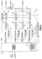
- the phase-change optical disc drive includes an optical head 10, recording pulse generation circuit 30 to generate a recording pulse, recording output control circuit 50 to control the recording pulse output and a semiconductor laser drive circuit 70 to drive a semiconductor laser 3 which will be discussed later.
- the optical disc 1 is spun at a constant angular velocity, for example, by a spindle motor 2 while the information recording surface of the optical disc 1 is being scanned with a laser light by the optical head 10, to optically record/reproduce information through the (1, 7) modulation.
- the semiconductor laser (LD) 3 is included in the optical head 10 to generate a reading/writing laser light for irradiation onto the optical disc 1.
- the laser light from the semiconductor laser 3 is formed to be a parallel beam by a collimator lens 4, passes through a side spot generating diffraction grating 5, and through a beam splitter 6 and quadrature wavelength plate (QWP) 7 and then it is incident upon an asphetic two-group objective lens 20 which will focus the laser light on the information recording surface of the optical disc 1.
- QWP quadrature wavelength plate
- the reflected light from the optical disc 1 (namely, reproduced signal) is reflected by the beam splitter 6 and led to the detection light path while a part of the reflected light is reflected by a beam splitter 11, passed through a condenser lens 12 and cylindrical lens 13 and incident upon a servo signal detector 14 where it is converted to a current while the rest of the reflected light from the optical disc 1 is passed through lenses 15 and 16 and incident upon an RF signal detector 17 where it is converted to a current.
- the astigmatism is used to generate a focus error signal and also the differential pushpull method is used to generate a tracking error signal.
- the two signal detectors 14 and 17 are used to detect servo error signal and reproduced RF signal, respectively. However, these signals can also be detected by a single detector.
- the aspheric two-group objective lens unit 20 includes a first electromagnetic actuator 22 to drive a first lens 21, and a second electromagnetic actuator 24 to drive a second lens 23.
- the second electromagnetic actuator 24 is movable in the optical-axial and tracking directions.
- the second lens 23 is mounted on the second electromagnetic actuator 24.
- the second lens 23 has an NA of about 0.5.
- the first lens 21 is provided above the second lens 23 and mounted on the first electromagnetic actuator 22 independent of the second electromagnetic actuator 23.
- the first lens 21 can be positioned on the optical axis.
- the first lens 21 is movable together with the second lens 23 in the tracking direction to follow up with the tracking servo control.
- a light beam from the semiconductor laser 3 is passed through these two objective lenses 23 and 21 by which it is focused on the phase-change information recording surface of the optical disc 1.
- the effective NA of the two-group objective lenses 23 and 21 is about 0.85.
- W 31 (n 2 - 1)n 2 sin ⁇ cos ⁇ /2(n 2 - sin 2 ⁇ ) 2/5 ⁇ tNA 3 / ⁇
- n refractive index of the disc substrate
- t Disc substrate thickness.
- the refractive index n is approximately a cube of the NA and proportional to the disc substrate thickness t.
- the disc substrate must be as thin as about 0.1 mm to assure a same skew tolerance as that of DVD-RAM.
- a phase-change recording medium on the disc substrate, a first dielectric layer (ZnS-SiO 2 ), recording layer (Ge 2 Sb 2 Te 5 ), second dielectric layer (ZnS-SiO 2 ) and a aluminum reflective layer are formed in this order on a disc substrate.
- a first dielectric layer ZnS-SiO 2
- recording layer Ga 2 Sb 2 Te 5
- second dielectric layer ZnS-SiO 2
- a aluminum reflective layer are formed in this order on a disc substrate.
- the optical disc 1 for use with the phase-change optical disc drive is produced by providing an aluminum reflective layer 1B, second dielectric layer 1C (ZnS-SiO 2 )a, recording layer 1D (Ge 2 Sb 2 Te 5 ), first dielectric layer 1E (ZnS-SiO 2 ) and Finally a disc protective layer 1F of 0.1 mm in thickness on a pre-formatted disc substrate 1A of 1.2 mm in thickness, as shown in FIG. 4.
- the order of forming the layers is opposite to that in production of the conventional optical disc.
- the recording pulse generation circuit 30 generates recording signals Data 1, Data 2 and Data 3 for generation of light pulses and an output control signal Data 3'.
- the recording pulse generation circuit 30 comprises a recording signal generation circuit 31 as shown in FIG. 5.
- the recording signal generation circuit 31 generates five kinds of recording signals including the above recording signal Data 1, NRZI (No Return to Zero Inverse) pulse enable signal, leading pulse enable signal, pulse train enable signal, and trailing pulse enable signal.
- the recording signal generation circuit 31 is switched between recording and reproduction modes by a CPU (not shown). When in the recording mode, this recording signal generation circuit 31 generates the above-mentioned five recording signals based on, for example, a 100-MHz master clock shown in FIG. 6(A) and NRZI signal shown in FIG. 6(B).
- the circuit 31 further comprises a channel clock sync pattern detection circuit 31a which judges, based on the NRZI signal, the length of the recording marks 3T to 11T, adjusts the delay time of each of variable delay elements 34, 37, 40 and 42 and thus determines a width of each pulse.
- the channel clock sync pattern detection circuit 31a similarly adjusts the delay time of each of variable delay elements 32, 35, 38 and 43 according to the judged recording mark length and thus sets a position of each pulse.
- the recording signal generation circuit 31 supplies the recording signal Data 1 to the variable delay element 32, NRZI pulse enable signal to a D flip-flop 33 and variable delay element 34, leading pulse enable signal to a D flip-flop 37 and variable delay element 37, pulse train enable signal to a D flip-flop 39, and the trailing pulse enable signal to a D flip-flop 41 and variable delay element 42.
- the variable delay element 32 delays the recording signal Data 1 a predetermined time and supplies it to the recording output control circuit 50.
- the recording signal Data 1 is a logic signal which is at H (high) level when the recording signal generation circuit 31 is in the recording or reproduction mode, and at L (low) level when no laser output is existent, as shown in FIG. 6(C).
- the D flip-flop 33 clears the NRZI pulse enable signal from the recording signal generation circuit 31 and supplies it to the variable delay element 35 which will delay the NRZI pulse enable signal a predetermined time and supplies it as an output control signal Data 3' (NRZI pulse) to an OR gate 45 and recording output control circuit 50.
- the output control signal Data 3' namely, the NRZI pulse, is the NRZI signal in FIG. 6(B) delayed a predetermined time as shown in FIGS. 6(F) and 6(G).
- the NRZI pulse length is 2T, 3T or 8T
- its width is 2T NRZIPW , 3T NRZIPW or 8T NRZIPW , respectively, which is determined by the variable delay element 34.
- the rise time of the NZRI pulse is delayed 2T NRZIPS , 3T NRZIPS or 8T NRZIPS from the NRZI signal of 2T, 3T or 8T, respectively, which is determined by the variable delay element 35.
- These NRZI pulses are used as output control pulse.
- the D flip-flop 36 clears the leading pulse enable signal from the recording signal generation circuit 31 and supplies it to the variable delay element 38 which will delay the leading pulse enable signal a predetermined time and supplies it to an OR gate 44.
- the D flip-flop 39 clears the pulse train enable signal from the recording signal generation circuit 31 and supplies it to the OR gate 44.
- the variable delay element 40 will delay the master clock from the recording signal generation circuit 31 a predetermined time and supplies it to the D flip-flop 39.
- the D flip-flop 41 clears the trailing pulse enable signal from the recording signal generation circuit 31 and supplies it to the variable delay element 43 which will delay the trailing pulse enable signal a predetermined time and supplies it to the OR gate 44.
- the OR gate 44 provides a logical sum of the pulses as the recording signal Data 3 and supplies it to the OR gate 45 and recording output control circuit 50.
- the recording signal Data 3 consists of a leading pulse, a train of n - 1 pulses and a trailing pulse for a recording mark having a length nT (n : integer from 2 to 8 and T : channel clock width), as shown in FIG. 6(E). Note that for a recording mark having a length 2T, the recording signal Data 3 consists only of the leading pulse.
- the OR gate 45 provides a logical sum of an inverted pulse of the output control signal Data 3' and the recording signal Data 3, and supplies it as a recording signal Data 2 to the recording output control circuit 50.
- the recording signal Data 2 is as shown in FIG. 6(D).
- the semiconductor laser drive circuit 70 drives the semiconductor laser 3 to generate a laser light according to the multi-pulse shown in FIG. 6(H).
- the aforementioned construction of the recording pulse generation circuit 30 is just an example, and it may be configured otherwise if it can generate the recording signals Data 1, Data 2 and Data 3 and the output control signal Data 3' shown in FIGS. 6(C) to 6(F).
- the recording output control circuit 50 comprises a photoelectric transducer circuit 51which transduces a current detected by the laser power monitoring detector 9 shown in FIG. 2 to a voltage to provide a LD control signal LDC, sample and hold circuits 52, 53 and 54 which sample and hold the LD control signal LDC, APC circuit 55 to control the signal level of the LD control signal LDC, delay elements 56 and 57 to delay a predetermined signal, sampled and held pulse select circuit 58 (will be referred to as "S&H select circuit” hereinbelow) which selects and provides a sampled and held pulse from the predetermined signal, data selector 59 which selects a desired one of the recording signals Data 1 to output control signal Data 3' and supplies it to the semiconductor laser drive circuit 70, and a CPU (Central Processing Unit) 60 which controls the above circuits.
- a photoelectric transducer circuit 51 which transduces a current detected by the laser power monitoring detector 9 shown in FIG. 2 to a voltage to provide a LD control signal LDC
- the photoelectric transducer circuit 51 supplies the sample and hold circuits 52, 53 and 54 with an LD control signal LDC obtained through the photoelectric transduction.
- the LD control signal LDC is detected a multi-pulse output obtained by the laser power monitoring detector 9.
- the sample and hold circuits 52, 53 and 54 sample the LD control signal LDC when the sampled and held pulse supplied from the S&H select circuit 58 is at H level, and hold the LD control signal LDC when the sampled and held pulse is at L level.
- the sample and hold circuits 52, 53 and 54 supply such LD control signals LDC (LDC 1, LDC 2 and LDC 3, respectively) to the APC circuit 55.
- the APC circuit 55 controls the LD control signals LDC 1, LDC2 and LDC 3 separately to a predetermined level and supplies them to the semiconductor laser drive circuit 70.
- the levels of the LD control signals LDC 1, LDC 2 and LDC 3 are set by the CPU 60.
- the LD control signal LDC 1 designates a reproduction power ("read power” in FIG. 6) at the time of data reproduction and an erasure power ("bias power 1" in FIG. 6) to erase data at the time of data recording.
- the LD control signal LDC 2 designates a cooling power ("bias power 2" in FIG. 6) at the time of data recording.
- the LD control signal LDC 3 designates a peak power ("peak power” in FIG. 6) at the time of data recording.
- the S&H select circuit 58 provides a predetermined sampling pulse to the sample and hold circuits 52, 53 and 54 under the control of the CPU 60.
- the S&H select circuit 58 supplies the sample and hold circuits 52, 53 and 54 with a L- or H-level sampling pulse, inverts an NRZI signal supplied via the delay element 56 and supplies it to the sample and hold circuit 53, and supplies the sample and hold circuit 54 with the output control signal Data 3' (NRZI pulse) supplied via the delay elements 56 and 57.
- the data selector 59 selects recording signals Data 1 to output control signal Data 3' and provide them as LD recording signals LD Data 1 to 3 or the LD recording signals LD Data 1 to 3 set to a predetermined level.
- the data selector 59 when in the recording power control mode, provides the recording signal Data 1 as LD recording signals LD Data 1, the LD recording signal LD Data 2 set to H level, and the output control signal Data 3' as LD recording signal LD Data 3.
- the data selector 59 When in the ordinary recording mode, provides the recording signal Data 1 as LD recording signal LD Data 1, the recording signal Data 2 as LD recording signal LD Data 2, and the recording signal Data 3 as LD control signal LDC 3
- the data selector 59 When in the reproduction mode, provides the recording signal Data 1 as LD recording signal LD Data 1 and the recording signal Data 1 as LED recording signal LD Data 1 and the LD data signal 2 set to L level. At this time, the data selector 59 will provide no LD control signal LDC 3.
- the data selector 59 does not provide the LD recording signals LD Data 1 and 3 but provides the LED recording signal LD Data 2 set to L level
- the recording output control circuit 50 When in the recording power control mode, the recording output control circuit 50 will adjust the LD control signals LDC 1, LDC 2 and LDC 3 as will be described below.
- the data selector 59 provides the recording signal Data 1 as LD recording signal LD Data 1 and fixes the LD recording signals LD Data 2 and 3 to L level.
- the S&H select circuit 58 supplies the sample and hold circuit 52 with a sampled and held pulse at H level.
- the sample and hold circuit 52 supplies the APC circuit 55 with the LD control signals LDC from the photoelectric transducer circuit 51.
- the APC circuit 55 will set the LD control signal LDC 1 from the sample and hold circuit 52 to a predetermined level under the control of the CPU 60.
- the S&H circuit 58 supplies the sample and hold circuit 52 at the enable terminal thereof with sampled and held pulse at L level.
- the LD control signal LDC 1 is fixed at L level.
- the data selector 59 provides the recording signal Data 1 as LD recording signal LD Data 1 and the output control signal Data 3' as LD recording signal LD Data 3, and fixes the LD recording signal LD Data 2 to H level.
- the S&H select circuit 58 supplies an inverted one of the NRZI signal to the enable terminal of the sample and hold circuit 53. Therefore, the sample and hold circuit 53 samples an output of the bias power 1 part and supplies it as LD control signal LDC 2 to the APC circuit 55.
- the bias power 1 being a laser power of the multi-pulse is sampled by the sample and hold circuit 53 and controlled by the APC circuit 55 as will be discussed later.
- the S&H select circuit 58 supplies an inverted one of the output control signal Data 3' (NRZI pulse) to the enable terminal of the sample and hold circuit 54. Therefore, the sample and hold circuit 54 samples the peak power of the multi-pulse and supplies it as LD control signal LDC 3 to the APC circuit 55. That is, the peak power being a laser power of the multi-pulse is sampled by the sample and hold circuit 54 and controlled by the APC circuit 55 as will be discussed later.
- the bias power 2 of the multi-pulse Since the bias power 2 of the multi-pulse has a same power as the read power, it is controlled based on a detected output of the RF signal during reproduction.
- the time of delay by the delay elements 56 and 57 corresponds to the time of delay by the semiconductor laser 3 and laser power monitoring detector 9 shown in FIG. 2.
- the APC circuit 55 sets the LD control signals LDC2 and LDC3 to a predetermined level under the control of the CPU 60.
- the S&H select circuit 58 supplies the sample and hold circuits 53 and 54 with an L-level sampled and held pulse and fixes the LD control signals LDC2 and LDC3 to the L level.
- the recording output control circuit 50 shifts to the ordinary recording mode.
- the data selector 59 will provide the recording signal Data 1 as LD recording signal LD Data 1, the recording signal Data 2 as LD recording signal LD Data 2, and the recording signal Data 3 as LD recording signal LD Data 3.
- the recording output control circuit 50 supplies the semiconductor laser drive circuit 70 with the NRZI pulse shown in FIG. 6(G) as LD recording signal LD Data 3, the semiconductor laser 3 is caused to generate a light beam according to the NRZI pulse.
- the recording output control circuit 50 samples and holds, according to the NRZI pulse, a peak power of a light beam detected by the laser power monitoring detector 9, so it is possible to control the laser beam power even for a multi-pulse of less than 10 ns in width. After completion of this light beam power control, data is recorded.
- the semiconductor laser drive circuit 70 comprises three current sources 71, 72 and 73 to supply a drive current to the semiconductor laser 3.
- the current sources 71, 72 and 73 are selectively controlled according to three kinds of LD recording signals LD Data 1 to 3 supplied from the recording output control circuit 50 and LD control signals LDC1 to LDC 3 corresponding to the LD recording signals to form a light waveform for the semiconductor laser 3.
- the LD control signal LDC 1 controls the operation of the first current source 71
- the LD control signal LDC 2 controls the operation of the second current source 72
- the LD control signal LDC 3 controls the operation of the third current source 73.
- Each of the LD control signals LDC is set to a predetermined value by the recording output control circuit 50, so that each of the currents from the first to third current sources 71 to 73 are set to a constant value.
- the semiconductor laser drive circuit 70 drives the semiconductor laser 3 to generate a multi-pulse according to the LD recording signals LD Data 1 to LD Data 3.
- the phase-change optical disc drive can sample and hold a peak power of a light beam detected by the laser power monitoring detector 9 according to the NRZI pulse when in the recording power control mode even for data recording at a user transfer rate higher than 30 Mbps, thereby controlling the laser power. Therefore, even during data recording in which the laser power may possibly vary under the influence of the return light from the optical disc 1, it is possible to stably control the peak power, bias power 1 and bias power 2 of the multi-pulse.
- a recording output sampling area is provided on the optical disc 1 to control each output of the multi-pulse by generating an appropriate NRZI pulse (for example, repetition of a 3T pattern).
- the above recording output sampling area may also be buried in an ordinary recorded data to set and control a recording power without any special area provided on the optical disc 1.
- the multi-pulse and NRZI pulse are different from each other in the rates at which the optical disc 1 is heated or cooled.
- appropriate methods of temperature compensation are available.
- the phase-change optical disc drive according to an embodiment of the present invention can control the pulse width to a predetermined value by the variable delay elements 34, 37, 40 and 42, respectively, and also the pulse position to a predetermined position by the variable delay elements 32, 35, 38 and 43 , respectively.
- the pulse width and laser irradiation position of the NRZI pulse and multi-pulse can be controlled correspondingly to recording marks 2T to 8T, respectively, the leading and trailing edges of the recording marks can be accurately controlled. That is, the quality of a reproduced signal will not be deteriorated.
- the present invention is not limited only to the embodiment having been described in the foregoing.
- the NRZI pulse is used as output control signal, but it may be a pulse having a larger width than the multi-pulse.
- an embodiment of the present invention may easily be built along with a wider-band and high-speed APC circuit in a large scale integrated circuit, thereby permitting to design a more compact circuit.
- the recording/reproducing apparatus and method for a phase-change optical disc can control the multi-pulse power even at a high transfer rate by generating an output control pulse having a larger width than the multi-pulse when in the power control mode, causes the semiconductor laser to generate a light pulse according to the output control pulse, samples and holds the laser power detected by the detecting means according to the output control pulse and controlling the laser power of the semiconductor laser so that the sampled and held laser power has a predetermined value.
Landscapes
- Physics & Mathematics (AREA)
- Optics & Photonics (AREA)
- Optical Head (AREA)
- Optical Recording Or Reproduction (AREA)
Applications Claiming Priority (2)
| Application Number | Priority Date | Filing Date | Title |
|---|---|---|---|
| JP1995798 | 1998-01-30 | ||
| JP10019957A JPH11213429A (ja) | 1998-01-30 | 1998-01-30 | 相変化型光ディスクの記録装置及び記録方法 |
Publications (2)
| Publication Number | Publication Date |
|---|---|
| EP0933759A2 true EP0933759A2 (fr) | 1999-08-04 |
| EP0933759A3 EP0933759A3 (fr) | 2001-01-10 |
Family
ID=12013687
Family Applications (1)
| Application Number | Title | Priority Date | Filing Date |
|---|---|---|---|
| EP99300457A Withdrawn EP0933759A3 (fr) | 1998-01-30 | 1999-01-21 | Enregistrement de données, et appareil d'entraínement de disque optique |
Country Status (3)
| Country | Link |
|---|---|
| US (1) | US6222814B1 (fr) |
| EP (1) | EP0933759A3 (fr) |
| JP (1) | JPH11213429A (fr) |
Cited By (7)
| Publication number | Priority date | Publication date | Assignee | Title |
|---|---|---|---|---|
| EP0978827A3 (fr) * | 1998-08-04 | 2001-01-10 | Hitachi, Ltd. | Procédé d'enregistrement d'informations, support d'enregistrement d'informations, et dispositif d'enregistrement d'informations |
| EP1136992A2 (fr) | 2000-03-24 | 2001-09-26 | Samsung Electronics Co., Ltd. | Dispositif et procédé de commande automatique de la puissance d'une diode laser |
| EP1073045A3 (fr) * | 1999-06-10 | 2003-01-08 | Samsung Electronics Co., Ltd. | Dispositif de lecture optique |
| EP1283520A3 (fr) * | 2001-08-07 | 2003-08-06 | Mitsumi Electric Company Ltd. | Lecteur de disque optique |
| US6678225B2 (en) | 1998-08-04 | 2004-01-13 | Hitachi, Ltd. | Information recording method, information recording medium and information recording apparatus |
| US6868053B2 (en) | 2000-04-12 | 2005-03-15 | Matsushita Electric Industrial Co., Ltd. | Optical information recording apparatus for stable recording |
| CN1321414C (zh) * | 2002-10-18 | 2007-06-13 | 三星电子株式会社 | 光拾取器和使用它的光学记录和/或再现装置 |
Families Citing this family (22)
| Publication number | Priority date | Publication date | Assignee | Title |
|---|---|---|---|---|
| JP4068752B2 (ja) | 1999-03-02 | 2008-03-26 | シャープ株式会社 | 光ディスク装置 |
| US6584050B1 (en) * | 1999-04-26 | 2003-06-24 | Sharp Kabushiki Kaisha | Optical recording device, optical reproducing device, and optical memory medium |
| KR100297789B1 (ko) * | 1999-06-03 | 2001-10-29 | 윤종용 | 다양한 형태의 광기록 매체에 적합한 기록 펄스 발생 방법 및이에 적합한 기록장치 |
| KR100322601B1 (ko) * | 1999-06-18 | 2002-03-18 | 윤종용 | 광디스크 기록 방법, 광디스크 기록 장치의 제어 방법 및 이에 적합한 광디스크 기록 장치 |
| US7272094B2 (en) * | 1999-07-15 | 2007-09-18 | Koninklike Philips Electronics N.V. | Methods and devices for recording marks in an information layer of an optical record carrier, and record carriers for use therein |
| ES2323941T3 (es) * | 2000-05-09 | 2009-07-28 | Koninklijke Philips Electronics N.V. | Procedimiento y dispositivo para grabar una señal de informacion en una capa de informacion de un medio de grabacion. |
| KR100434488B1 (ko) * | 2001-02-19 | 2004-06-05 | 삼성전자주식회사 | 광 기록 펄스 발생 장치 및 방법 |
| JP2002298350A (ja) * | 2001-03-28 | 2002-10-11 | Tdk Corp | 光記録方法、光記録装置及び光記録媒体 |
| KR100442860B1 (ko) * | 2001-05-17 | 2004-08-02 | 삼성전자주식회사 | 레이저 다이오드 출력 제어 장치 |
| KR20030028369A (ko) * | 2001-09-29 | 2003-04-08 | 삼성전자주식회사 | 광 기록매체에 데이터를 기록하는 방법 및 그 장치 |
| WO2003034410A1 (fr) * | 2001-10-17 | 2003-04-24 | Tdk Corporation | Support d'enregistrement optique et procede pour enregistrer des informations sur un support d'enregistrement optique |
| DE60221333T2 (de) | 2001-10-22 | 2008-04-17 | Ricoh Co., Ltd. | Treibereinheit einer Lichtquelle und optische Speichervorrichtung |
| JP4142338B2 (ja) * | 2002-05-09 | 2008-09-03 | 富士フイルム株式会社 | 光情報記録方法 |
| JP3961886B2 (ja) * | 2002-06-06 | 2007-08-22 | パイオニア株式会社 | 情報記録装置 |
| JP3931133B2 (ja) * | 2002-10-29 | 2007-06-13 | 株式会社日立製作所 | 光ディスク装置および位相調整方法 |
| KR100493033B1 (ko) * | 2002-11-12 | 2005-06-07 | 삼성전자주식회사 | 레이저 파워 제어 장치 |
| KR100510544B1 (ko) * | 2003-08-28 | 2005-08-26 | 삼성전자주식회사 | 광 구동기에 있어서 레이저 다이오드 파워 제어 장치 |
| US20050083828A1 (en) * | 2003-10-17 | 2005-04-21 | Chih-Yuan Chen | Apparatus and method for laser power control |
| JP4564960B2 (ja) * | 2004-07-07 | 2010-10-20 | パイオニア株式会社 | 情報記録装置、情報記録方法及び情報記録プログラム |
| CN1301503C (zh) * | 2005-01-14 | 2007-02-21 | 威盛电子股份有限公司 | 可消除光驱读写头的输出功率偏移的功率控制方法 |
| JP2006236421A (ja) * | 2005-02-22 | 2006-09-07 | Toshiba Corp | 記憶媒体、再生方法及び記録方法 |
| US20060239153A1 (en) * | 2005-04-25 | 2006-10-26 | Mediatek Incorporation | Methods and circuits for automatic power control |
Family Cites Families (13)
| Publication number | Priority date | Publication date | Assignee | Title |
|---|---|---|---|---|
| JPH07111782B2 (ja) * | 1986-08-13 | 1995-11-29 | ソニー株式会社 | 光デイスクの記録再生装置 |
| US4845720A (en) * | 1987-10-20 | 1989-07-04 | Matsushita Electric Industrial Co., Ltd. | Semiconductor laser control circuit |
| US5059780A (en) * | 1989-09-07 | 1991-10-22 | Pioneer Electronic Corporation | Light power control circuit for a semiconductor light-emitting element |
| US5642343A (en) * | 1990-06-29 | 1997-06-24 | Hitachi, Ltd. | Magnetooptic disc apparatus and recording medium |
| US5260956A (en) * | 1991-09-30 | 1993-11-09 | Nikon Corporation | Laser drive circuit |
| US5347505A (en) * | 1992-01-20 | 1994-09-13 | Fujitsu Limited | Optical medium recording method and apparatus employing pulse width delay and/or advancement |
| JPH0684224A (ja) * | 1992-09-07 | 1994-03-25 | Hitachi Ltd | 光磁気ディスクの記録制御方法 |
| JP3477770B2 (ja) * | 1992-12-16 | 2003-12-10 | 松下電器産業株式会社 | レーザパワー制御装置及び制御方法 |
| US5490126A (en) * | 1993-04-07 | 1996-02-06 | Matsushita Electric Industrial Co., Ltd. | Apparatus for recording and reproducing data on a disk |
| JPH09107144A (ja) * | 1995-10-11 | 1997-04-22 | Sony Corp | レーザダイオードの劣化判定回路 |
| US5636179A (en) * | 1996-02-09 | 1997-06-03 | Iowa State University Research Foundation | Sonic spectrometer and treatment system |
| JPH09330519A (ja) * | 1996-06-10 | 1997-12-22 | Hitachi Ltd | 光ディスク記録再生装置 |
| JP3608926B2 (ja) * | 1996-12-26 | 2005-01-12 | 株式会社日立製作所 | 情報記録装置 |
-
1998
- 1998-01-30 JP JP10019957A patent/JPH11213429A/ja not_active Withdrawn
-
1999
- 1999-01-21 EP EP99300457A patent/EP0933759A3/fr not_active Withdrawn
- 1999-01-27 US US09/237,531 patent/US6222814B1/en not_active Expired - Fee Related
Cited By (16)
| Publication number | Priority date | Publication date | Assignee | Title |
|---|---|---|---|---|
| US7349318B2 (en) | 1998-08-04 | 2008-03-25 | Hitachi, Ltd. | Information recording method, information recording medium and information recording apparatus |
| EP0978827A3 (fr) * | 1998-08-04 | 2001-01-10 | Hitachi, Ltd. | Procédé d'enregistrement d'informations, support d'enregistrement d'informations, et dispositif d'enregistrement d'informations |
| US8040777B2 (en) | 1998-08-04 | 2011-10-18 | Hitachi, Ltd. | Information recording method, information recording medium and information recording apparatus |
| US6678225B2 (en) | 1998-08-04 | 2004-01-13 | Hitachi, Ltd. | Information recording method, information recording medium and information recording apparatus |
| EP2015300A1 (fr) * | 1998-08-04 | 2009-01-14 | Hitachi, Ltd. | Procédé d'enregistrement d'informations, appareil d'enregistrement d'informations et support d'enregistrement d'informations |
| US6925040B1 (en) | 1998-08-04 | 2005-08-02 | Hitachi, Ltd. | Information recording method, information recording medium and information recording apparatus |
| US7352675B2 (en) | 1998-08-04 | 2008-04-01 | Hitachi, Ltd. | Information recording method, information recording medium and information recording apparatus |
| US7349317B2 (en) | 1998-08-04 | 2008-03-25 | Hitachi, Ltd. | Information recording method, information recording medium and information recording apparatus |
| EP1073045A3 (fr) * | 1999-06-10 | 2003-01-08 | Samsung Electronics Co., Ltd. | Dispositif de lecture optique |
| US6731586B2 (en) | 2000-03-24 | 2004-05-04 | Samsung Electronics Co., Ltd. | Apparatus for and method of controlling auto laser diode power |
| EP1136992A2 (fr) | 2000-03-24 | 2001-09-26 | Samsung Electronics Co., Ltd. | Dispositif et procédé de commande automatique de la puissance d'une diode laser |
| EP1136992A3 (fr) * | 2000-03-24 | 2006-09-06 | Samsung Electronics Co., Ltd. | Dispositif et procédé de commande automatique de la puissance d'une diode laser |
| US7113473B2 (en) | 2000-04-12 | 2006-09-26 | Matsushita Electric Industrial Co., Ltd. | Optical information recording apparatus for stable recording |
| US6868053B2 (en) | 2000-04-12 | 2005-03-15 | Matsushita Electric Industrial Co., Ltd. | Optical information recording apparatus for stable recording |
| EP1283520A3 (fr) * | 2001-08-07 | 2003-08-06 | Mitsumi Electric Company Ltd. | Lecteur de disque optique |
| CN1321414C (zh) * | 2002-10-18 | 2007-06-13 | 三星电子株式会社 | 光拾取器和使用它的光学记录和/或再现装置 |
Also Published As
| Publication number | Publication date |
|---|---|
| JPH11213429A (ja) | 1999-08-06 |
| EP0933759A3 (fr) | 2001-01-10 |
| US6222814B1 (en) | 2001-04-24 |
Similar Documents
| Publication | Publication Date | Title |
|---|---|---|
| US6222814B1 (en) | Recording/reproducing apparatus and method for phase-change optical disc | |
| US8773963B2 (en) | Highly adaptive recording method and optical recording apparatus | |
| EP0669611B1 (fr) | Méthode et appareil d'enregistrement d'information optique | |
| KR100337945B1 (ko) | 정보기록방법, 정보기록매체 및 정보기록장치 | |
| US7813239B2 (en) | Optical information recording method, optical information recording device and optical information recording medium | |
| US7301875B2 (en) | Information recording device and information recording method | |
| JP2000076653A (ja) | 情報記録装置 | |
| JPH11120563A (ja) | 光ディスクの記録補償方法及び光ディスク記録装置 | |
| JP2002358646A (ja) | 光学的情報記録再生方式、およびその記録媒体と装置 | |
| HK1076661B (en) | Information recording device and information recording method | |
| JP2001229540A (ja) | 光情報記録再生方法および光情報記録再生装置 |
Legal Events
| Date | Code | Title | Description |
|---|---|---|---|
| PUAI | Public reference made under article 153(3) epc to a published international application that has entered the european phase |
Free format text: ORIGINAL CODE: 0009012 |
|
| AK | Designated contracting states |
Kind code of ref document: A2 Designated state(s): DE FR GB |
|
| AX | Request for extension of the european patent |
Free format text: AL;LT;LV;MK;RO;SI |
|
| PUAL | Search report despatched |
Free format text: ORIGINAL CODE: 0009013 |
|
| AK | Designated contracting states |
Kind code of ref document: A3 Designated state(s): AT BE CH CY DE DK ES FI FR GB GR IE IT LI LU MC NL PT SE |
|
| AX | Request for extension of the european patent |
Free format text: AL;LT;LV;MK;RO;SI |
|
| RIC1 | Information provided on ipc code assigned before grant |
Free format text: 7G 11B 7/125 A, 7G 11B 7/00 B |
|
| 17P | Request for examination filed |
Effective date: 20010615 |
|
| AKX | Designation fees paid |
Free format text: DE FR GB |
|
| STAA | Information on the status of an ep patent application or granted ep patent |
Free format text: STATUS: THE APPLICATION IS DEEMED TO BE WITHDRAWN |
|
| 18D | Application deemed to be withdrawn |
Effective date: 20060801 |