EP0933861A1 - Stromversorgungsschaltung zur Erzeugung von positiven und negativen Spannungen - Google Patents
Stromversorgungsschaltung zur Erzeugung von positiven und negativen Spannungen Download PDFInfo
- Publication number
- EP0933861A1 EP0933861A1 EP99102020A EP99102020A EP0933861A1 EP 0933861 A1 EP0933861 A1 EP 0933861A1 EP 99102020 A EP99102020 A EP 99102020A EP 99102020 A EP99102020 A EP 99102020A EP 0933861 A1 EP0933861 A1 EP 0933861A1
- Authority
- EP
- European Patent Office
- Prior art keywords
- voltage
- source
- output
- power source
- negative
- Prior art date
- Legal status (The legal status is an assumption and is not a legal conclusion. Google has not performed a legal analysis and makes no representation as to the accuracy of the status listed.)
- Withdrawn
Links
- 230000015654 memory Effects 0.000 abstract description 27
- 239000003990 capacitor Substances 0.000 description 16
- 238000006243 chemical reaction Methods 0.000 description 10
- 230000006870 function Effects 0.000 description 5
- 239000004065 semiconductor Substances 0.000 description 5
- 230000008859 change Effects 0.000 description 4
- 238000010586 diagram Methods 0.000 description 4
- 230000000087 stabilizing effect Effects 0.000 description 3
- 238000004519 manufacturing process Methods 0.000 description 2
- 238000000034 method Methods 0.000 description 2
- 230000008569 process Effects 0.000 description 2
- 230000001052 transient effect Effects 0.000 description 2
- 230000004075 alteration Effects 0.000 description 1
- 230000000295 complement effect Effects 0.000 description 1
- 239000000470 constituent Substances 0.000 description 1
- 230000007547 defect Effects 0.000 description 1
- 230000000694 effects Effects 0.000 description 1
- 230000004048 modification Effects 0.000 description 1
- 238000012986 modification Methods 0.000 description 1
- 238000005086 pumping Methods 0.000 description 1
- 230000009467 reduction Effects 0.000 description 1
- 230000005641 tunneling Effects 0.000 description 1
Images


Classifications
-
- G—PHYSICS
- G11—INFORMATION STORAGE
- G11C—STATIC STORES
- G11C16/00—Erasable programmable read-only memories
- G11C16/02—Erasable programmable read-only memories electrically programmable
- G11C16/06—Auxiliary circuits, e.g. for writing into memory
-
- H—ELECTRICITY
- H02—GENERATION; CONVERSION OR DISTRIBUTION OF ELECTRIC POWER
- H02M—APPARATUS FOR CONVERSION BETWEEN AC AND AC, BETWEEN AC AND DC, OR BETWEEN DC AND DC, AND FOR USE WITH MAINS OR SIMILAR POWER SUPPLY SYSTEMS; CONVERSION OF DC OR AC INPUT POWER INTO SURGE OUTPUT POWER; CONTROL OR REGULATION THEREOF
- H02M3/00—Conversion of DC power input into DC power output
- H02M3/02—Conversion of DC power input into DC power output without intermediate conversion into AC
- H02M3/04—Conversion of DC power input into DC power output without intermediate conversion into AC by static converters
- H02M3/06—Conversion of DC power input into DC power output without intermediate conversion into AC by static converters using resistors or capacitors, e.g. potential divider
- H02M3/07—Conversion of DC power input into DC power output without intermediate conversion into AC by static converters using resistors or capacitors, e.g. potential divider using capacitors charged and discharged alternately by semiconductor devices with control electrode, e.g. charge pumps
- H02M3/073—Charge pumps of the Schenkel-type
-
- G—PHYSICS
- G11—INFORMATION STORAGE
- G11C—STATIC STORES
- G11C16/00—Erasable programmable read-only memories
- G11C16/02—Erasable programmable read-only memories electrically programmable
- G11C16/06—Auxiliary circuits, e.g. for writing into memory
- G11C16/30—Power supply circuits
Definitions
- the present invention relates to a power source for generating positive and negative voltage sources and, more particularly to the control of a power source circuit which generates a voltage source having a polarity inverse to the polarity of the source voltage supplied to the semiconductor device.
- Flash memories are increasingly used as nonvolatile memory devices for storing programs and data.
- a potential difference as high as 16 to 18 volts is generally applied between the source and the control gate of the memory cell.
- the control gate is applied with 16 to 18 volts while maintaining the source potential of the memory transistor at zero volt.
- the circuit line connected to the control gate must have a withstand voltage of 16 to 18 volts, which results in a large chip size due to a large element dimension for obtaining a large withstand voltage.
- a negative voltage source is also used in a flash memory to reduce the potential of the positive voltage source applied to the control gate. For example, if the source voltage is -4 volts, 12 volts is sufficient for the control gate voltage to obtain a voltage difference of 16 volts. This remarkably reduces the withstand voltage of the control gate as well as the control circuit for the control gate, thereby reducing the element dimensions and the chip size of the flash memory. For this reason, a negative voltage source is generally required in the semiconductor device having a flash memory.
- Figs. 1A and 1B show the voltages applied for programming and erasing, respectively, a memory cell in a flash memory by using a known Fowler-Nordheim (F-N) tunneling effect.
- F-N Fowler-Nordheim
- the amount of electrons injected or withdrawn into/from the floating gate varies with the fluctuation of the negative voltage. For example, if the applied voltage is above -4 volts, the amount of injected electrons is less than the designed amount, which results in an eventual programmed state shifting from the erased state in the memory cell due to the leakage of the electrons with the lapse of time. This defect must be avoided in the flash memory to prevent the erroneous data from occurring by stabilizing the negative voltage source in the semiconductor device.
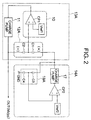
- Patent Publication JP-A-7-231647 proposes a power source circuit used in a flash memory, such as shown in Fig. 2.
- the power source circuit includes a positive source section 14A for generating a positive voltage source and a negative source section 13A for generating a negative voltage source.
- the positive source section 14A has a charge pump 17 and a comparator CP2 for comparing the output of a voltage divider 19A, which includes capacitors C3 and C4 for dividing the output potential of the charge pump 17, against a reference voltage Vref2 for a feedback control of the charge pump 17.
- the positive source section 14A generates a positive voltage of 12 volts, for example.
- the negative source section 13A has a control unit 10, a charge pump 11 and a voltage divider 12A including serial capacitors C1 and C2.
- the control unit 10 has a comparator CP1 for comparing the output of the voltage divider 12A dividing the voltage difference between the output of the charge pump 17 and the output of the charge pump 11 against a reference voltage Vref1.
- the capacitances of the capacitors C1 and C2 are designed such that the output of the voltage divider 12A is positive.
- the charge pump 11 is activated to lower the output voltage of the charge pump 11, whereas if the output of the voltage divider 12A is lower than the reference voltage Vref1, the charge pump 11 is inactivated to stop the lowering of the output voltage thereof.
- the output voltage NVpp of the negative source section 13A is clumped at a constant negative voltage NVpp for use in programming or erasing memory cells in a flash memory.
- the output voltage NVpp of the negative source section 13A is controlled by feedback of the output of the voltage divider 12A.
- the output voltage of the positive source section 14A is unstable until a considerable length of time elapses since the supplied power source is turned on for the power source circuit. Since the negative source section 13A starts before the output of the positive source section 12A becomes stable, in the transient period after the power source is turned on, both the outputs of the positive source section 14A and the negative circuit section 13A are unstable. This prolongs the time length for stabilizing by which the power source circuit generates a stable negative output voltage NVpp.
- the fluctuation of the negative output voltage NVpp is transferred during a transient state to the output of the positive source section 14A through the voltage divider 12A, the output of which is also transferred to the non-inverting input of the comparator CP2 and to the input of the charge pump 17. The voltage fluctuations thus transferred further prolong the time length for stabilizing the negative output voltage NVpp.
- the present invention provides a power source circuit comprising a first source section for generating a first voltage source having a first polarity, a second source section for generating a second voltage source having a second polarity opposing the first polarity, an impedance converter for receiving the second voltage source to generate a third voltage source having an output impedance different from an output impedance of the first voltage source, a first voltage divider for dividing a voltage difference between the third voltage source and the first voltage source to generate a first divided voltage having the second polarity, and a control unit for controlling a voltage of the first voltage source by maintaining the first divided voltage at a first reference voltage.
- the impedance converter suppresses the change of the output of the first voltage divider, whereby the fluctuation of the first voltage source can be stabilized in a short time after the supplied power source is turned on for the power source circuit.
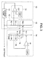
- a power source circuit for use in a flash memory includes a positive source section 14, a negative source section 13, and an impedance conversion section 15.
- the positive circuit section 14 includes a differential amplifier 18, an output transistor TR1, a voltage compensator 16 including an n-channel transistor TR2 having a drain and a gate connected together, and a voltage divider 19 including serial resistors R1 and R2.
- the output transistor TR1, voltage compensating transistor TR3 and the voltage divider 19 are serially connected between a source line and the ground.
- the differential amplifier 18 has an inverting input connected to the output of the voltage divider 19, a non-inverting input supplied with a positive reference voltage Vref2, and an output terminal connected to the gate of the output transistor TR1.
- the impedance conversion section 15 is implemented by an n-channel transistor TR2 forming a source follower.
- the drain of the output transistor TR1 delivers the output voltage of the positive source section 14, which is supplied to the gate of the transistor TR2 in the impedance conversion section 15.
- the negative source section 13 includes a control unit 10 implemented by a comparator CP1, a voltage divider 12, and a charge pump 11.
- the voltage divider 12 including serial resistors R1 and R2 and n-channel transistor TR2 in the impedance conversion section 15 are serially connected in this order between the source line and the output terminal of the charge pump 11.
- the comparator CP1 has an inverting input connected to a referenced voltage Vref1, a non-inverting input connected to the output of the voltage divider 12, and an output terminal connected to the control input of the charge pump 11, the output of which constitutes the output terminal OUT of the negative source section 13.
- the output of the voltage divider 12 is a positive voltage obtained by dividing the difference between the drain potential of the transistor TR2 and the output potential of the negative source section 13.
- the source potential of the transistor TR2 is equal to the output of the positive source section 14 minus the threshold voltage Vth of the source follower transistor TR2, which is equal to the threshold voltage of the voltage compensating transistor TR3.
- the voltage compensating transistor TR3 compensates the voltage drop across the source follower transistor TR2.
- a MOS transistor having a drain and a gate connected together has a source voltage equal to the gate voltage minus the threshold voltage Vth of the MOS transistor.
- the differential amplifier 18 functions for maintaining the potential of the output node “C” or the source voltage of the output transistor TR1 without the voltage compensator 16, the source voltage of the source follower transistor TR2 or the potential of node “A” varies depending on the threshold voltage Vth of the source follower transistor TR2, which generally varies depending on the fabrication process or the ambient temperature for the power source circuit.
- the charge pump 11 shown in Fig. 3 includes a plurality of serial MOS transistors Q1, Q2, ⁇ Qn connected in this order between the ground and the output terminal of the negative source section 13, and a plurality of capacitors C1, C2, ⁇ Cn disposed for respective transistors Q1, Q2, ⁇ Qn.
- Each of the MOS transistors Q1, Q2, ⁇ Qn has a source and a gate connected together.
- Each of the odd-numbered capacitors C1, C3, ⁇ Cn-1 is connected between the source of a corresponding one of the transistors Q1, Q3, ⁇ Qn-1 and a first clock line receiving a clock signal ⁇ n
- each of the even-numbered capacitors C2, C4, ⁇ Cn is connected between the source of a corresponding one of the transistors Q2, Q4, ⁇ Qn and a second clock line receiving an inverted clock signal/ ⁇ n, which is complementary with the clock signal ⁇ n.
- the clock signals ⁇ n and / ⁇ n are supplied to the capacitors C1, C3, ⁇ Cn-1 and capacitors C2, C4, ⁇ Cn, respectively, during the interval when the output of the comparator CP1 stays at the H-level.
- the rise of the clock signal ⁇ n is temporarily transmitted through the odd-numbered capacitors C1, C3, ⁇ , whereby the potentials of nodes I, K ⁇ , or the source voltages of odd-numbered transistors Q1, Q3 ⁇ , rises from the previous potential level by the amplitude of the clock pulse in the clock signal ⁇ n.
- transistor Q1 turns on to transfer the electric charge stored in the capacitor C1 to the ground.
- transistor Q3 turns on to transfer the electric charge stored in the capacitor C3 to the capacitor C2.
- the electric charge is transferred from the output terminal OUT to the ground by a pumping function of the charge pump 11, thereby generating a negative voltage source NVpp.
- the comparator CP1 compares the output of the voltage divider 12 against the reference voltage Vref1, and delivers a H-level if the output of the voltage divider 12 is higher than the reference voltage Vref1. As a result, the charge pump 11 starts for operation to lower the negative output voltage NVpp. If the output of the voltage divider 12 is lower than the reference voltage Vref1, the comparator CP1 delivers a L-level, whereby the charge pump 11 stops the operation. In these operations, the output voltage NVpp of the negative source section 13 converges to and is maintained at -9 volts, for example, which is used for programming or erasing memory cells in the flash memory.
- the source follower configuration of the impedance conversion transistor TR2, connected between the positive source line and the voltage divider 12, functions for lowering the output impedance of the positive voltage source, whereby the current flowing through the voltage divider 12 generates less change in the output voltage of the positive source section 14.
- the positive source section 14 does not include a charge pump as used in the conventional power source circuit, the output of the positive source section 14 becomes stable in a short time after the start of the power source circuit, whereby the output voltage of the negative source section 13 also becomes stable in a short time.
- the impedance conversion section 15 functions for a buffer amplifier, whereby a temporary potential change of the output terminal OUT of the negative source section 13 less affects the output voltage of the positive source section 14, by limiting the influence of the change only to the output voltage of the negative source section 13. As a result, if the output negative voltage NVpp changes due to an external factor, the output negative voltage converges to the designed potential in a short time.
- the functions of the voltage compensation section 16 is more specifically described hereinafter.
- the potential of the inverting input of the differential amplifier 18 converges exactly to the reference voltage Vref2 by the feedback loop including the differential amplifier 18.
- the output potential of the positive source section 14 is equal to the sum of the reference voltage Vref2 and the voltage drop across the resistor R3 and the threshold voltage Vth of the voltage compensating transistor TR3. Therefore, the source potential of the transistor TR2 of the impedance conversion section 15 is equal to the output of the positive source section 14 minus the threshold voltage Vth of the transistor TR2, which is designed equal to the threshold voltage of the transistor TR3.
- the output potential of the impedance conversion section 15 is equal to the threshold voltage Vth plus the voltage drop across the resistor R3, and does not fluctuate irrespective of the process conditions of the fabrication or the ambient temperature of the power source circuit.
- the voltage compensating transistor TR3 may be omitted if the variation of the threshold voltage Vth of the source follower transistor TR2 of the impedance conversion section 15 is negligibly small.
- the dividing ratio of the resistors R3 and R4 may be changed in consideration of reduction in the output potential of the transistor TR2 by the threshold Vth, thereby maintaining the potential of node "A" equal to the case of the illustrated embodiment.
- a positive voltage source is provided to the power source circuit from outside the semiconductor device, whereby the control unit 10 and the differential amplifier 18 operate on the positive voltage source to generate a negative output voltage.
- the control unit 10 and the differential amplifier 18 are designed to operate on the negative voltage source to generate a positive output voltage together with a charge pump.
- the MOS transistors as used in the embodiment may be replaced by bipolar transistors.
- the terms "drain”, “gate” and “source” as used in this text refer to collector, base and emitter of the bipolar transistor.
- the impedance conversion section 15 may be an emitter follower transistor instead of the source follower transistor.
Landscapes
- Engineering & Computer Science (AREA)
- Power Engineering (AREA)
- Read Only Memory (AREA)
- Continuous-Control Power Sources That Use Transistors (AREA)
- Dc-Dc Converters (AREA)
Applications Claiming Priority (2)
| Application Number | Priority Date | Filing Date | Title |
|---|---|---|---|
| JP2200698 | 1998-02-03 | ||
| JP2200698A JPH11219596A (ja) | 1998-02-03 | 1998-02-03 | 半導体装置の電源回路 |
Publications (1)
| Publication Number | Publication Date |
|---|---|
| EP0933861A1 true EP0933861A1 (de) | 1999-08-04 |
Family
ID=12070930
Family Applications (1)
| Application Number | Title | Priority Date | Filing Date |
|---|---|---|---|
| EP99102020A Withdrawn EP0933861A1 (de) | 1998-02-03 | 1999-02-01 | Stromversorgungsschaltung zur Erzeugung von positiven und negativen Spannungen |
Country Status (5)
| Country | Link |
|---|---|
| US (1) | US6084387A (de) |
| EP (1) | EP0933861A1 (de) |
| JP (1) | JPH11219596A (de) |
| KR (1) | KR100283872B1 (de) |
| CN (1) | CN1228599A (de) |
Families Citing this family (31)
| Publication number | Priority date | Publication date | Assignee | Title |
|---|---|---|---|---|
| US6441765B1 (en) | 2000-08-22 | 2002-08-27 | Marvell International, Ltd. | Analog to digital converter with enhanced differential non-linearity |
| US6396334B1 (en) | 2000-08-28 | 2002-05-28 | Marvell International, Ltd. | Charge pump for reference voltages in analog to digital converter |
| US6400214B1 (en) | 2000-08-28 | 2002-06-04 | Marvell International, Ltd. | Switched capacitor filter for reference voltages in analog to digital converter |
| US6417725B1 (en) | 2000-08-28 | 2002-07-09 | Marvell International, Ltd. | High speed reference buffer |
| US6369554B1 (en) * | 2000-09-01 | 2002-04-09 | Marvell International, Ltd. | Linear regulator which provides stabilized current flow |
| JP2004164811A (ja) * | 2002-09-26 | 2004-06-10 | Sharp Corp | 半導体記憶装置および携帯電子機器 |
| US6841980B2 (en) * | 2003-06-10 | 2005-01-11 | Bae Systems, Information And Electronic Systems Integration, Inc. | Apparatus for controlling voltage sequencing for a power supply having multiple switching regulators |
| KR100515060B1 (ko) * | 2003-08-13 | 2005-09-14 | 삼성전자주식회사 | 비트 라인의 프리차지 레벨을 일정하게 유지하는 불휘발성반도체 메모리 장치 |
| JP4040575B2 (ja) | 2003-12-19 | 2008-01-30 | 三菱電機株式会社 | 電圧発生回路 |
| KR100605590B1 (ko) | 2004-05-10 | 2006-07-31 | 주식회사 하이닉스반도체 | 데이터 출력드라이버의 임피던스를 조정할 수 있는 반도체메모리 장치 |
| CN2750356Y (zh) * | 2004-11-20 | 2006-01-04 | 鸿富锦精密工业(深圳)有限公司 | 线性稳压电源 |
| US7489910B2 (en) * | 2005-03-30 | 2009-02-10 | Kabushiki Kaisha Toshiba | Wireless transmitter and amplifier |
| KR100675014B1 (ko) * | 2006-02-24 | 2007-01-29 | 삼성전자주식회사 | 온도센서를 위한 전력공급장치 |
| JP4895694B2 (ja) * | 2006-06-08 | 2012-03-14 | ルネサスエレクトロニクス株式会社 | 電源回路 |
| CN100428105C (zh) * | 2006-08-25 | 2008-10-22 | 清华大学 | 1v电源非线性纠正的高温度稳定性基准电压源 |
| JP2008107971A (ja) * | 2006-10-24 | 2008-05-08 | Elpida Memory Inc | 電源電圧発生回路および半導体集積回路装置 |
| JP5112753B2 (ja) * | 2007-06-08 | 2013-01-09 | セイコーインスツル株式会社 | チャージポンプ回路 |
| JP4660526B2 (ja) | 2007-09-21 | 2011-03-30 | 株式会社東芝 | 負電圧検知回路を備えた半導体集積回路 |
| JP5479218B2 (ja) * | 2010-05-20 | 2014-04-23 | ルネサスエレクトロニクス株式会社 | 昇圧回路 |
| JP5087670B2 (ja) * | 2010-11-01 | 2012-12-05 | 株式会社東芝 | 電圧発生回路 |
| JP2012210063A (ja) * | 2011-03-29 | 2012-10-25 | Yamaha Corp | 電圧変換回路 |
| CN103138564A (zh) * | 2011-11-30 | 2013-06-05 | 上海华虹Nec电子有限公司 | 电荷泵输出电压温度补偿电路 |
| US8830776B1 (en) | 2013-03-15 | 2014-09-09 | Freescale Semiconductor, Inc. | Negative charge pump regulation |
| CN105468075B (zh) * | 2015-12-22 | 2017-10-24 | 上海华虹宏力半导体制造有限公司 | 负压电荷泵反馈电路 |
| JP6817053B2 (ja) * | 2016-12-13 | 2021-01-20 | ラピスセミコンダクタ株式会社 | チャージポンプ回路及び昇圧回路 |
| KR102392661B1 (ko) * | 2017-07-18 | 2022-04-29 | 삼성전자주식회사 | 비휘발성 메모리 장치의 전압 생성기, 비휘발성 메모리 장치 및 비휘발성 메모리 장치의 동작 방법 |
| JP6794395B2 (ja) * | 2018-03-09 | 2020-12-02 | 株式会社東芝 | 半導体装置 |
| CN109164863B (zh) * | 2018-08-28 | 2020-06-09 | 上海华虹宏力半导体制造有限公司 | Sonos栅端控制电压产生电路 |
| US10910072B1 (en) | 2019-12-17 | 2021-02-02 | Sandisk Technologies Llc | Accurate self-calibrated negative to positive voltage conversion circuit and method |
| US12362001B2 (en) * | 2022-08-26 | 2025-07-15 | Changxin Memory Technologies, Inc. | Voltage generating circuit and memory |
| CN119448765B (zh) * | 2025-01-07 | 2025-05-02 | 上海安其威微电子科技有限公司 | 负压源切换电路和射频开关芯片 |
Citations (6)
| Publication number | Priority date | Publication date | Assignee | Title |
|---|---|---|---|---|
| US5168174A (en) * | 1991-07-12 | 1992-12-01 | Texas Instruments Incorporated | Negative-voltage charge pump with feedback control |
| WO1994028629A1 (en) * | 1993-05-28 | 1994-12-08 | Macronix International Co., Ltd. | Negative voltage generator for flash eprom design |
| JPH07231647A (ja) * | 1994-02-15 | 1995-08-29 | Mitsubishi Electric Corp | 半導体装置 |
| FR2735885A1 (fr) * | 1995-06-21 | 1996-12-27 | Sgs Thomson Microelectronics | Circuit generateur de tension negative du type pompe de charge comprenant un circuit de regulation |
| EP0807936A2 (de) * | 1996-05-10 | 1997-11-19 | Nec Corporation | Für die Löschspannungsversorgung einer Flash-Speicherzelle geeignete nichtflüchtige Halbleiterspeichernanordnung |
| JPH103794A (ja) * | 1996-06-12 | 1998-01-06 | Hitachi Ltd | 不揮発性記憶装置および駆動方法 |
Family Cites Families (2)
| Publication number | Priority date | Publication date | Assignee | Title |
|---|---|---|---|---|
| JP3417630B2 (ja) * | 1993-12-17 | 2003-06-16 | 株式会社日立製作所 | 半導体集積回路装置とフラッシュメモリ及び不揮発性記憶装置 |
| DE69312305T2 (de) * | 1993-12-28 | 1998-01-15 | Sgs Thomson Microelectronics | Spannungsbooster, insbesondere für nichtflüchtige Speicher |
-
1998
- 1998-02-03 JP JP2200698A patent/JPH11219596A/ja active Pending
-
1999
- 1999-02-01 EP EP99102020A patent/EP0933861A1/de not_active Withdrawn
- 1999-02-02 KR KR1019990003451A patent/KR100283872B1/ko not_active Expired - Fee Related
- 1999-02-03 CN CN99100572A patent/CN1228599A/zh active Pending
- 1999-02-03 US US09/243,550 patent/US6084387A/en not_active Expired - Fee Related
Patent Citations (6)
| Publication number | Priority date | Publication date | Assignee | Title |
|---|---|---|---|---|
| US5168174A (en) * | 1991-07-12 | 1992-12-01 | Texas Instruments Incorporated | Negative-voltage charge pump with feedback control |
| WO1994028629A1 (en) * | 1993-05-28 | 1994-12-08 | Macronix International Co., Ltd. | Negative voltage generator for flash eprom design |
| JPH07231647A (ja) * | 1994-02-15 | 1995-08-29 | Mitsubishi Electric Corp | 半導体装置 |
| FR2735885A1 (fr) * | 1995-06-21 | 1996-12-27 | Sgs Thomson Microelectronics | Circuit generateur de tension negative du type pompe de charge comprenant un circuit de regulation |
| EP0807936A2 (de) * | 1996-05-10 | 1997-11-19 | Nec Corporation | Für die Löschspannungsversorgung einer Flash-Speicherzelle geeignete nichtflüchtige Halbleiterspeichernanordnung |
| JPH103794A (ja) * | 1996-06-12 | 1998-01-06 | Hitachi Ltd | 不揮発性記憶装置および駆動方法 |
Also Published As
| Publication number | Publication date |
|---|---|
| CN1228599A (zh) | 1999-09-15 |
| US6084387A (en) | 2000-07-04 |
| KR100283872B1 (ko) | 2001-02-15 |
| JPH11219596A (ja) | 1999-08-10 |
| KR19990072379A (ko) | 1999-09-27 |
Similar Documents
| Publication | Publication Date | Title |
|---|---|---|
| US6084387A (en) | Power source circuit for generating positive and negative voltage sources | |
| US6771547B2 (en) | Boosted voltage generating circuit and semiconductor memory device having the same | |
| US6567309B2 (en) | Semiconductor device | |
| US6356499B1 (en) | Power supply circuit and semiconductor memory device having the same | |
| KR100462270B1 (ko) | Mos 충전펌프 발생 및 레귤레이션 방법 및 장치 | |
| JPH01259751A (ja) | 昇圧回路 | |
| US6201434B1 (en) | Semiconductor integrated circuit device having an oscillation circuit using reference current source independent from influence of variation of power supply voltage and threshold voltage of transistor | |
| US6788577B2 (en) | Nonvolatile semiconductor memory | |
| KR0167872B1 (ko) | 반도체장치의 내부전원회로 | |
| JPH0793022B2 (ja) | 半導体メモリ集積回路 | |
| US7576523B2 (en) | Power supply circuit and semiconductor memory | |
| US6735119B2 (en) | Nonvolatile semiconductor memory | |
| JP3314951B2 (ja) | 電荷ポンプ回路 | |
| JPH0778471A (ja) | 半導体集積回路 | |
| JP3979268B2 (ja) | 不揮発性半導体メモリの内部電源回路及び不揮発性半導体メモリ装置 | |
| CN119380788B (zh) | 位线电压传输电路 | |
| JP2916364B2 (ja) | 半導体装置の内部電源回路 | |
| KR19980071727A (ko) | 반도체 집적 회로 | |
| JP2000040385A (ja) | 半導体装置 |
Legal Events
| Date | Code | Title | Description |
|---|---|---|---|
| PUAI | Public reference made under article 153(3) epc to a published international application that has entered the european phase |
Free format text: ORIGINAL CODE: 0009012 |
|
| AK | Designated contracting states |
Kind code of ref document: A1 Designated state(s): DE FR GB |
|
| AX | Request for extension of the european patent |
Free format text: AL;LT;LV;MK;RO;SI |
|
| 17P | Request for examination filed |
Effective date: 19990928 |
|
| AKX | Designation fees paid |
Free format text: DE FR GB |
|
| STAA | Information on the status of an ep patent application or granted ep patent |
Free format text: STATUS: THE APPLICATION HAS BEEN WITHDRAWN |
|
| 18W | Application withdrawn |
Effective date: 20030207 |