EP0935371A2 - Jeu de registres à portes multiples pour le mise à jour des coéfficients d'un filter RIF opérant en mode rafale - Google Patents
Jeu de registres à portes multiples pour le mise à jour des coéfficients d'un filter RIF opérant en mode rafale Download PDFInfo
- Publication number
- EP0935371A2 EP0935371A2 EP98309952A EP98309952A EP0935371A2 EP 0935371 A2 EP0935371 A2 EP 0935371A2 EP 98309952 A EP98309952 A EP 98309952A EP 98309952 A EP98309952 A EP 98309952A EP 0935371 A2 EP0935371 A2 EP 0935371A2
- Authority
- EP
- European Patent Office
- Prior art keywords
- memory
- significant bits
- coefficients
- output
- updating
- Prior art date
- Legal status (The legal status is an assumption and is not a legal conclusion. Google has not performed a legal analysis and makes no representation as to the accuracy of the status listed.)
- Granted
Links
Images
Classifications
-
- H—ELECTRICITY
- H04—ELECTRIC COMMUNICATION TECHNIQUE
- H04L—TRANSMISSION OF DIGITAL INFORMATION, e.g. TELEGRAPHIC COMMUNICATION
- H04L25/00—Baseband systems
- H04L25/02—Details ; arrangements for supplying electrical power along data transmission lines
- H04L25/03—Shaping networks in transmitter or receiver, e.g. adaptive shaping networks
- H04L25/03006—Arrangements for removing intersymbol interference
- H04L25/03012—Arrangements for removing intersymbol interference operating in the time domain
- H04L25/03114—Arrangements for removing intersymbol interference operating in the time domain non-adaptive, i.e. not adjustable, manually adjustable, or adjustable only during the reception of special signals
- H04L25/03133—Arrangements for removing intersymbol interference operating in the time domain non-adaptive, i.e. not adjustable, manually adjustable, or adjustable only during the reception of special signals with a non-recursive structure
-
- G—PHYSICS
- G06—COMPUTING OR CALCULATING; COUNTING
- G06F—ELECTRIC DIGITAL DATA PROCESSING
- G06F17/00—Digital computing or data processing equipment or methods, specially adapted for specific functions
- G06F17/10—Complex mathematical operations
-
- H—ELECTRICITY
- H03—ELECTRONIC CIRCUITRY
- H03H—IMPEDANCE NETWORKS, e.g. RESONANT CIRCUITS; RESONATORS
- H03H17/00—Networks using digital techniques
- H03H17/02—Frequency selective networks
- H03H17/0223—Computation saving measures; Accelerating measures
- H03H17/0227—Measures concerning the coefficients
-
- H—ELECTRICITY
- H03—ELECTRONIC CIRCUITRY
- H03H—IMPEDANCE NETWORKS, e.g. RESONANT CIRCUITS; RESONATORS
- H03H21/00—Adaptive networks
- H03H21/0012—Digital adaptive filters
Definitions
- This invention relates to adaptive finite impulse response (FIR) filters, and more particularly, to adaptive FIR filters using time multiplexed multipliers with multiple coefficients per multiplier and which implement burst mode updating of the filter coefficients.
- FIR finite impulse response
- FIR filters employ fixed delay lines for recirculating the coefficients. Such delay lines are implemented using a series of edge triggered flip flops. As a result, in operation, the prior art delay lines consume more power than is desirable.
- a multiported register file is a memory, typically small, e.g., having a capacity for four words, with at least one read port and one write port. Data written into the multiported register file may be read out therefrom in any desired order.
- the multiported register file may have additional output ports from which the data stored therein may be read out, also in any desired order, and independent from the order of any other output port.
- each multiported register file feeds data from one output to the multiply-add portion of its associated stage of the FIR filter. Note that these outputs may be the same. For coefficient use, there is no need to operate the register file in the lookthrough mode described in the copending application.
- the FIR filter is an adaptive filter with updatable coefficients, it is necessary to have an update unit which computes new coefficient values.
- multiported register files of the prior copending application circulated all of the bits of the coefficients all of the time. Each bit of the coefficient that is circulated requires incremental power consumption.
- multiported register files may be used for storing coefficients in adaptive FIR filters.
- the multiported register files of prior copending application are improved upon by implementing a split memory architecture, with the ability to separately control the least significant bits and the most significant bits of coefficient values that are stored in the filter.
- burst mode updating--such as disclosed in United States Patent No.
- split architecture and disabling techniques may be used to provide advantages in architectures that use recirculating registers, such as the aforementioned
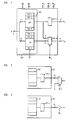
- FIG. 1 shows an exemplary multiported register file which may be used for coefficient storage in a stage of a finite impulse response filter (FIR), in accordance with the principles of the invention.
- a multiported register file is a memory, typically small, e.g., having a capacity for four words, with at least one read port and one write port. Data written into the multiported register file may be read out therefrom in any desired order.
- the multiported register file may have additional output ports from which the data stored therein may be read out, also in any desired order, and independent from the order of any other output port.
- FIG. 1 shows multiported register file 101, including a) memory locations 102, which is divided into memory locations 103, including memory locations 103-1 through 103-H and memory locations 104, including memory locations 104-1 through 104-H, b) computation unit 105, and c) latches 107, including latches 107-1 through 107-K.
- Memory locations 103 are used to store the most significant bits of each of the coefficients stored in one of memory locations 102, while memory locations 104 are used to store the least significant bits of each of the coefficients stored in one of memory locations 102.
- each of memory locations 102 has a "split" architecture, being split between its most significant bits and its least significant bits.
- the number of bits supplied by multiported register file 101 to a multiplier of the FIR filter into which it incorporated is the number of bits stored in each of memory locations 103.
- the remaining bits of each coefficient are stored in each of memory locations 104.
- the ones of locations of memory location 103 and 104 that have the same suffix correspond to the same one of memory locations 102, and thus to the same coefficient.
- all of the bits of a coefficient including both those stored in one of memory locations 103 and 104, are employed when the coefficient is updated, if it is updated.
- the number of memory locations in the multiported register file is typically a small number, e.g., 4. Having a small value of H allows efficient FIR filter implementations-compared with other alternatives for implementing FIR filters-for processing signals having a sample rate that is within an order of magnitude of the fastest clock frequencies in the system, such as is found in modems for use in broadband access.
- Data is written to multiported register file 101 via write port W, which includes N data lines.
- the particular one of memory locations 102 to which data presented at write port W is written to is specified by write address WA. More particularly, the P most significant bits are written to the one of memory locations 103 specified by write address WA, and similarly, the Q least significant bits are written to the one of memory locations 104 specified by write address WA.
- When and whether data is written to multiported register file 101 is a function of the value of write enable signal WE.
- WE has a first value data is written to multiported register file 101.
- WE has the complementary value of the first value data is not written to multiported register file 101.
- Data is read from multiported register file 101 via any of read ports R, including read ports R 1 through R K .
- Each of read ports R 1 through R K includes a respective number of data lines M 1 through M k . If desired, a less precise representation of a value stored in multiported register file 101 may be read out therefrom.
- the particular one of memory locations 103 and 104 from which data is read for presentation to any one of read ports R 1 through R K is specified by an address supplied to the corresponding, e.g., like numbered, one of read address ports RA 1 through RA k .
- write address WA, and read address RA 1 through RA k have the same number of address lines, L.
- a read enable signal is provided on one or more of read ports R 1 through R K to prevent unwanted data reads which can cause unnecessary power consumption.
- Data may be written to and read from multiported register file 101 at the same time. More specifically, data may be written to and read from the same particular one of memory locations 102 at the same time. Thus, a first value may be written to a particular one of memory locations 102 while at the same time a different value may be read from that very same particular location and supplied to one, or more, of read ports R 1 through R K .
- a first value may be written to a particular one of memory locations 102 while at the same time a different value may be read from that very same particular location and supplied to one, or more, of read ports R 1 through R K .
- only the most significant bits of a coefficient, stored in one of memory locations 103 may be supplied to a particular one of read ports R 1 through R K .
- Latches 107 are conventional level sensitive latches such as are described by N. Weste and K. Eshraghian on pages 19-21 of Principles of CMOS VLSI Design, 2nd Ed., Addison Wesley, 1992, which is incorporated by reference as if fully set forth herein. Thus, any one of memory locations 103 may act as a master latch while any one of latches 107 may act as a slave latch to form an edge triggered flip-flop.
- read port R 1 reads out only the most significant bits of a coefficient which are stored in memory locations 103.
- read port R K reads all the bits of a coefficient stored in memory location 102, but only supplies an output to read port R k when read enable signal RE is in a particular stage, e.g., when RE is high. At all other times, the value of read port R K remains static at the last value stored in latch 107-K.
- the effect of read enable signal RE may be implemented in the register file by gating, e.g., AND gating, the read enable signal and the clock which is used for accessing memory locations 102.
- a read enable may be used in conjunction with memory locations 104.
- the read enable signal has a specified value, e.g., high, no coefficient least significant bit values are read out of memory locations 104, regardless of the presence of valid read addresses at any of read address ports RA 1 through RA k .
- burst mode coefficient updating updates coefficients when errors exceed a predetermined threshold while leaving the coefficients unchanged when errors are less than a predetermined threshold.
- burst mode coefficient updating may be implemented efficiently as follows.
- a read enable signal RE for the reading of memory locations 104 is enabled, e.g., set high, so that data is read out from memory locations 104.
- the read enable control signal RE k for read port R k is used to read out from memory locations 102 coefficient values already stored therein.
- the write enable WE control signal is enabled to write into memory locations 102 updated coefficient values which are supplied from a coefficient updating unit in a conventional manner.
- the write enable WE control signal and the read enable control signal RE k for read port R k are disabled, e.g., set to a low value. As a result, no changes occur in the data appearing at the output of read port R k . In other words, the data appearing at the output of read port R k remains constant.
- This may be implemented by gating, e.g., AND gating, read enable control signal RE k with the clock used for controlling latches 107, and using the gated signal as the clock for latch 107-K.
- a read enable signal RE for the reading of memory locations 104 is disabled, e.g., set low, so that data is not read out from memory locations 104.
- This may be implemented by gating, e.g., AND gating, read enable control signal RE with the clock used for memory locations 102, and using the gated signal as the clock for memory 104.
- the power consumed by memory locations 102 is reduced, by on order of about 50%, when coefficients are not being updated. This can result in a significant power savings, as a goal of burst mode updating is to minimize the time during which coefficient updating takes place.
- the output of read port R k is supplied to updating circuitry, e.g., an adder. If there are changes occurring in the data supplied to updating circuitry, as in the prior art, then computations are performed by the updating circuitry. Such computations inherently consume power. However, by not supplying changing data to the updating circuit, in accordance with the principles of the invention, such power consumption is avoided, as the inputs to the updating circuitry remain static, and so does its output.
- updating circuitry e.g., an adder.
- the total filter power consumption may be reduced by more than half.
- read enable signal RE to disable reading, and hence changes, from memory 104
- it is only necessary to separately disable the most significant bits from reaching the updating circuitry e.g., by using read enable control signal RE k to control only the latching of by latch 107-K of the most significant bits from memory 103.
- an optional computation unit such as disclosed in copending United States Patent Application Serial No. (Case Larsson 5-12), may be incorporated between memory locations 102 and one or more of output ports R 1 through R K .
- an external multiplexer can be used to supply as an output a constant value when coefficients are not being updated.
- a constant value means the same value which is fixedly input to one input port of the multiplexer.
- a tri-state driver may be used.
- a read enable signal REi is used to control the respective multiplexer or driver.
- a bus-keeper circuit may be used in conjunction with the tri-state driver to insure that the previous value of a coefficient remains on the lines to the update unit.
- the value that remains on the lines to the update unit is referred to as a steady value.
- split architecture and disabling techniques may be used to provide advantages in architectures that use recirculating registers, such as in the aforementioned United States Patent No. 5,646,957.
- substantially the same results can be obtained by having two separate multiported register files, one for the most significant bits and one for the least significant bits. These multiported register files would be supplied with the same read and write signals, as appropriate.
- Such an architecture is more costly, in that it requires extra decoders, such as, read address decoders and write address decoders.
Landscapes
- Engineering & Computer Science (AREA)
- Power Engineering (AREA)
- Computer Networks & Wireless Communication (AREA)
- Signal Processing (AREA)
- Complex Calculations (AREA)
- Filters That Use Time-Delay Elements (AREA)
- Use Of Switch Circuits For Exchanges And Methods Of Control Of Multiplex Exchanges (AREA)
- Static Random-Access Memory (AREA)
- Executing Machine-Instructions (AREA)
- Cable Transmission Systems, Equalization Of Radio And Reduction Of Echo (AREA)
Applications Claiming Priority (2)
| Application Number | Priority Date | Filing Date | Title |
|---|---|---|---|
| US08/996,869 US6785327B1 (en) | 1997-12-23 | 1997-12-23 | Multiported register file for burst mode coefficient updating |
| US996869 | 1997-12-23 |
Publications (3)
| Publication Number | Publication Date |
|---|---|
| EP0935371A2 true EP0935371A2 (fr) | 1999-08-11 |
| EP0935371A3 EP0935371A3 (fr) | 2000-10-04 |
| EP0935371B1 EP0935371B1 (fr) | 2004-04-14 |
Family
ID=25543386
Family Applications (1)
| Application Number | Title | Priority Date | Filing Date |
|---|---|---|---|
| EP98309952A Expired - Lifetime EP0935371B1 (fr) | 1997-12-23 | 1998-12-04 | Jeu de registres à portes multiples pour l'enregistrement des coéfficients d'un filter RIF adaptif |
Country Status (8)
| Country | Link |
|---|---|
| US (1) | US6785327B1 (fr) |
| EP (1) | EP0935371B1 (fr) |
| JP (1) | JP3380759B2 (fr) |
| KR (1) | KR100657417B1 (fr) |
| CN (1) | CN1235415A (fr) |
| BR (1) | BR9805454A (fr) |
| CA (1) | CA2254543A1 (fr) |
| DE (1) | DE69823158T2 (fr) |
Cited By (1)
| Publication number | Priority date | Publication date | Assignee | Title |
|---|---|---|---|---|
| EP4030388A1 (fr) * | 2017-04-21 | 2022-07-20 | Intel Corporation | Mélange de points fixes dédiés pour efficacité énergétique |
Families Citing this family (5)
| Publication number | Priority date | Publication date | Assignee | Title |
|---|---|---|---|---|
| WO2013084367A1 (fr) * | 2011-12-07 | 2013-06-13 | 日本電気株式会社 | Dispositif de traitement de signal d'égalisation, dispositif récepteur optique et procédé de traitement de signal d'égalisation l'employant |
| KR101391352B1 (ko) | 2011-12-19 | 2014-05-07 | 삼성전자주식회사 | 메모리 시스템 및 그것의 프로그램 방법 |
| US9509321B2 (en) * | 2013-11-27 | 2016-11-29 | Microchip Technology Incorporated | Main clock high precision oscillator |
| KR101453950B1 (ko) * | 2014-02-24 | 2014-11-04 | 엘아이지넥스원 주식회사 | 다중 모드 수신기를 위한 ddc의 운영 방법 |
| KR101453949B1 (ko) | 2014-02-24 | 2014-10-23 | 엘아이지넥스원 주식회사 | 다중 모드 수신기를 위한 ddc |
Family Cites Families (10)
| Publication number | Priority date | Publication date | Assignee | Title |
|---|---|---|---|---|
| US4605826A (en) * | 1982-06-23 | 1986-08-12 | Nec Corporation | Echo canceler with cascaded filter structure |
| US4967340A (en) * | 1985-06-12 | 1990-10-30 | E-Systems, Inc. | Adaptive processing system having an array of individually configurable processing components |
| US5117385A (en) * | 1990-03-16 | 1992-05-26 | International Business Machines Corporation | Table lookup multiplier with digital filter |
| JPH04302522A (ja) * | 1991-03-29 | 1992-10-26 | Hitachi Ltd | 演算回路及びこれを用いた適応フィルタ並びにエコーキャンセラ |
| US5396517A (en) * | 1993-03-04 | 1995-03-07 | Adtran | Transversal filter useable in echo canceler, decision feedback equalizer applications for minimizing non-linear distortion in signals conveyed over full duplex two-wire communication link |
| EP0665998A4 (fr) * | 1993-08-03 | 1996-06-12 | Xilinx Inc | Circuit fpga a microprocesseur. |
| US5646957A (en) * | 1995-07-28 | 1997-07-08 | Lucent Technologies Inc. | Burst update for an adaptive equalizer |
| US5721696A (en) * | 1995-08-28 | 1998-02-24 | Motorola Inc. | Method and system for performing an FIR filtering operation |
| US6112291A (en) * | 1997-01-24 | 2000-08-29 | Texas Instruments Incorporated | Method and apparatus for performing a shift instruction with saturate by examination of an operand prior to shifting |
| US6377619B1 (en) * | 1997-09-26 | 2002-04-23 | Agere Systems Guardian Corp. | Filter structure and method |
-
1997
- 1997-12-23 US US08/996,869 patent/US6785327B1/en not_active Expired - Lifetime
-
1998
- 1998-11-26 CA CA002254543A patent/CA2254543A1/fr not_active Abandoned
- 1998-12-04 DE DE69823158T patent/DE69823158T2/de not_active Expired - Lifetime
- 1998-12-04 EP EP98309952A patent/EP0935371B1/fr not_active Expired - Lifetime
- 1998-12-18 BR BR9805454-6A patent/BR9805454A/pt not_active Application Discontinuation
- 1998-12-22 CN CN98123224A patent/CN1235415A/zh active Pending
- 1998-12-22 JP JP36362198A patent/JP3380759B2/ja not_active Expired - Fee Related
- 1998-12-23 KR KR1019980057459A patent/KR100657417B1/ko not_active Expired - Fee Related
Cited By (1)
| Publication number | Priority date | Publication date | Assignee | Title |
|---|---|---|---|---|
| EP4030388A1 (fr) * | 2017-04-21 | 2022-07-20 | Intel Corporation | Mélange de points fixes dédiés pour efficacité énergétique |
Also Published As
| Publication number | Publication date |
|---|---|
| US6785327B1 (en) | 2004-08-31 |
| KR100657417B1 (ko) | 2007-05-14 |
| BR9805454A (pt) | 1999-11-09 |
| EP0935371B1 (fr) | 2004-04-14 |
| DE69823158T2 (de) | 2005-04-14 |
| JPH11266143A (ja) | 1999-09-28 |
| KR19990063346A (ko) | 1999-07-26 |
| EP0935371A3 (fr) | 2000-10-04 |
| CA2254543A1 (fr) | 1999-06-23 |
| CN1235415A (zh) | 1999-11-17 |
| DE69823158D1 (de) | 2004-05-19 |
| JP3380759B2 (ja) | 2003-02-24 |
Similar Documents
| Publication | Publication Date | Title |
|---|---|---|
| EP0905890B1 (fr) | Structure de filtre | |
| EP1176718B1 (fr) | Accélérateur en hardware pour l'adaptation des coéfficients basée sur l'algorithme de la moyenne des plus petits carrés | |
| JPH0222423B2 (fr) | ||
| JPH06222908A (ja) | 多数の多ビット要素を含む複合オペランドに対して並列的に算術演算を実行する方法 | |
| US4215416A (en) | Integrated multiplier-accumulator circuit with preloadable accumulator register | |
| EP0097779B1 (fr) | Circuit logique | |
| EP0935371B1 (fr) | Jeu de registres à portes multiples pour l'enregistrement des coéfficients d'un filter RIF adaptif | |
| US5301139A (en) | Shifter circuit for multiple precision division | |
| US5432944A (en) | Data processing system having a dynamically enabled input synchronizer for selectively minimizing power consumption | |
| US6857065B2 (en) | System and method for system initializating a data processing system by selecting parameters from one of a user-defined input, a serial non-volatile memory and a parallel non-volatile memory | |
| Agarwal et al. | Series approximation methods for divide and square root in the Power3/sup TM/processor | |
| US6542539B1 (en) | Multiported register file for coefficient use in filters | |
| KR100712864B1 (ko) | 디지털 필터 계수의 동적 범위를 변화시키는 시스템 | |
| US5880607A (en) | Clock distribution network with modular buffers | |
| Moloney et al. | Low-power 200-Msps, area-efficient, five-tap programmable FIR filter [in BiCMOS] | |
| US6178472B1 (en) | Queue having distributed multiplexing logic | |
| US7129755B2 (en) | High-fanin static multiplexer | |
| US5351207A (en) | Methods and apparatus for subtraction with 3:2 carry-save adders | |
| Bartlett et al. | A low-power asynchronous VLSI FIR filter | |
| US6941418B1 (en) | Integrated circuit and method outputting data | |
| JP3166781B2 (ja) | 加算回路 | |
| Chen et al. | Self-timed dynamically pipelined adaptive signal processing system: a case study of DLMS equalizer for read channel | |
| EP1269345B1 (fr) | Filtre numerique a ondes | |
| US20040260742A1 (en) | Arithmetic circuit | |
| US20060101364A1 (en) | Method and apparatus for data distribution in a high speed processing unit |
Legal Events
| Date | Code | Title | Description |
|---|---|---|---|
| PUAI | Public reference made under article 153(3) epc to a published international application that has entered the european phase |
Free format text: ORIGINAL CODE: 0009012 |
|
| 17P | Request for examination filed |
Effective date: 19981224 |
|
| AK | Designated contracting states |
Kind code of ref document: A2 Designated state(s): DE FR GB |
|
| AX | Request for extension of the european patent |
Free format text: AL;LT;LV;MK;RO;SI |
|
| PUAL | Search report despatched |
Free format text: ORIGINAL CODE: 0009013 |
|
| AK | Designated contracting states |
Kind code of ref document: A3 Designated state(s): AT BE CH CY DE DK ES FI FR GB GR IE IT LI LU MC NL PT SE |
|
| AX | Request for extension of the european patent |
Free format text: AL;LT;LV;MK;RO;SI |
|
| RIC1 | Information provided on ipc code assigned before grant |
Free format text: 7H 04L 25/03 A, 7H 03H 21/00 B |
|
| 17Q | First examination report despatched |
Effective date: 20001222 |
|
| AKX | Designation fees paid | ||
| RBV | Designated contracting states (corrected) |
Designated state(s): DE FR GB |
|
| REG | Reference to a national code |
Ref country code: DE Ref legal event code: 8566 |
|
| RTI1 | Title (correction) |
Free format text: MULTIPORTED REGISTER FILE FOR STORING COEFFICIENTS FOR USE IN AN ADAPTIVE FIR FILTER |
|
| GRAP | Despatch of communication of intention to grant a patent |
Free format text: ORIGINAL CODE: EPIDOSNIGR1 |
|
| GRAS | Grant fee paid |
Free format text: ORIGINAL CODE: EPIDOSNIGR3 |
|
| GRAA | (expected) grant |
Free format text: ORIGINAL CODE: 0009210 |
|
| AK | Designated contracting states |
Kind code of ref document: B1 Designated state(s): DE FR GB |
|
| REG | Reference to a national code |
Ref country code: GB Ref legal event code: FG4D |
|
| REF | Corresponds to: |
Ref document number: 69823158 Country of ref document: DE Date of ref document: 20040519 Kind code of ref document: P |
|
| ET | Fr: translation filed | ||
| PLBE | No opposition filed within time limit |
Free format text: ORIGINAL CODE: 0009261 |
|
| STAA | Information on the status of an ep patent application or granted ep patent |
Free format text: STATUS: NO OPPOSITION FILED WITHIN TIME LIMIT |
|
| 26N | No opposition filed |
Effective date: 20050117 |
|
| PGFP | Annual fee paid to national office [announced via postgrant information from national office to epo] |
Ref country code: FR Payment date: 20131209 Year of fee payment: 16 |
|
| REG | Reference to a national code |
Ref country code: DE Ref legal event code: R082 Ref document number: 69823158 Country of ref document: DE Representative=s name: DILG HAEUSLER SCHINDELMANN PATENTANWALTSGESELL, DE |
|
| REG | Reference to a national code |
Ref country code: FR Ref legal event code: ST Effective date: 20150831 |
|
| PG25 | Lapsed in a contracting state [announced via postgrant information from national office to epo] |
Ref country code: FR Free format text: LAPSE BECAUSE OF NON-PAYMENT OF DUE FEES Effective date: 20141231 |
|
| PGFP | Annual fee paid to national office [announced via postgrant information from national office to epo] |
Ref country code: DE Payment date: 20151119 Year of fee payment: 18 Ref country code: GB Payment date: 20151125 Year of fee payment: 18 |
|
| REG | Reference to a national code |
Ref country code: DE Ref legal event code: R119 Ref document number: 69823158 Country of ref document: DE |
|
| GBPC | Gb: european patent ceased through non-payment of renewal fee |
Effective date: 20161204 |
|
| PG25 | Lapsed in a contracting state [announced via postgrant information from national office to epo] |
Ref country code: GB Free format text: LAPSE BECAUSE OF NON-PAYMENT OF DUE FEES Effective date: 20161204 Ref country code: DE Free format text: LAPSE BECAUSE OF NON-PAYMENT OF DUE FEES Effective date: 20170701 |