EP0936574A2 - Ic-Karte und Ic-Kartensystem - Google Patents
Ic-Karte und Ic-Kartensystem Download PDFInfo
- Publication number
- EP0936574A2 EP0936574A2 EP99102543A EP99102543A EP0936574A2 EP 0936574 A2 EP0936574 A2 EP 0936574A2 EP 99102543 A EP99102543 A EP 99102543A EP 99102543 A EP99102543 A EP 99102543A EP 0936574 A2 EP0936574 A2 EP 0936574A2
- Authority
- EP
- European Patent Office
- Prior art keywords
- card
- circuit
- data sequence
- antenna
- transmission signal
- Prior art date
- Legal status (The legal status is an assumption and is not a legal conclusion. Google has not performed a legal analysis and makes no representation as to the accuracy of the status listed.)
- Withdrawn
Links
Images
Classifications
-
- G—PHYSICS
- G06—COMPUTING OR CALCULATING; COUNTING
- G06K—GRAPHICAL DATA READING; PRESENTATION OF DATA; RECORD CARRIERS; HANDLING RECORD CARRIERS
- G06K19/00—Record carriers for use with machines and with at least a part designed to carry digital markings
- G06K19/06—Record carriers for use with machines and with at least a part designed to carry digital markings characterised by the kind of the digital marking, e.g. shape, nature, code
- G06K19/067—Record carriers with conductive marks, printed circuits or semiconductor circuit elements, e.g. credit or identity cards also with resonating or responding marks without active components
- G06K19/07—Record carriers with conductive marks, printed circuits or semiconductor circuit elements, e.g. credit or identity cards also with resonating or responding marks without active components with integrated circuit chips
- G06K19/0723—Record carriers with conductive marks, printed circuits or semiconductor circuit elements, e.g. credit or identity cards also with resonating or responding marks without active components with integrated circuit chips the record carrier comprising an arrangement for non-contact communication, e.g. wireless communication circuits on transponder cards, non-contact smart cards or RFIDs
-
- G—PHYSICS
- G06—COMPUTING OR CALCULATING; COUNTING
- G06K—GRAPHICAL DATA READING; PRESENTATION OF DATA; RECORD CARRIERS; HANDLING RECORD CARRIERS
- G06K7/00—Methods or arrangements for sensing record carriers, e.g. for reading patterns
- G06K7/0008—General problems related to the reading of electronic memory record carriers, independent of its reading method, e.g. power transfer
Definitions
- the present invention relates to an IC card and an IC card system and, more particularly, to an IC card which transmits in a non-contact manner a signal modulated with desired data and to an IC card system using the IC card.
- IC card systems using IC cards have been applied to ticket examination systems for use in transport facilities, room entry/exit control systems, etc.
- An IC card system of this kind has been proposed which is constituted of IC cards carried by users and a read/writer (i.e., IC card processor) for exchanging various sorts of data with each of the IC cards.
- Various sorts of data are transmitted and received between the IC card and the read/writer in a non-contact manner.
- the read/writer forms a transmission signal by modulating a carrier having a predetermined frequency with a desired data sequence, and sends out the transmission signal to the IC card via an antenna.
- the IC card receives the transmission signal via an antenna and demodulates the transmission signal to reproduce the data sent from the read/writer. Further, the IC card sends out data such as personal information stored therein to the read/writer in response to the received data by modulating a predetermined carrier with the data to be transmitted.
- the read/writer receives the data sent from the IC card, and opens or closes a door of a ticket examination machine or allows entry into or exit from a room.
- a type of IC card for such use has been proposed which is arranged to send out desired data to a read/writer by the method of changing the power radiated from the antenna by changing the load impedance of the antenna (hereinafter referred to as "load switching system").
- a transmission signal sent from the read/writer is induced and this transmission signal is reradiated. If at this time the load impedance of the antenna is changed, the reradiated power is correspondingly changed. Then, in the receiving antenna coupled to the antenna of the IC card, the carrier of the transmission signal is detected at the signal level corresponding to the change in the load impedance.
- desired data can be sent out by being modulated in an amplitude shift keying (ASK) manner based on a simple arrangement.
- ASK amplitude shift keying
- This kind of IC card is carried by a user and is brought close to the read/writer when used. Therefore, the signal level of the transmitted signal induced in the antenna varies largely depending upon use.
- a method of processing the signal obtained from the antenna by clamping the signal may be used. If such a method is used, the power reradiated by following the change in the load impedance cannot be sufficiently changed. That is, the degree of amplitude shift keying modulation is reduced, resulting in a deterioration in data quality.
- an object of the present invention to provide an IC card and an IC card system capable of performing data exchange without a semiconductor device having a sufficiently large withstand voltage while being arranged as simply as the load switching system.
- an IC card in which a reference signal having the same frequency as a carrier of a transmission signal received by an antenna and phase-synchronized with the carrier is formed, and in which a response data sequence is sent out from the antenna by modulating the reference signal with the response data sequence in a phase shift keying (PSK) manner.
- PSK phase shift keying
- an IC card in which the load on a power supply circuit for producing operating power by rectifying a transmission signal received by an antenna is changed according to a response data sequence.
- an IC card system constituted of each of the above-described IC cards.
- an IC card in which a reference signal having the same frequency as a carrier of a transmission signal received by an antenna and phase-synchronized with the carrier is formed, and in which the reference signal is selectively sent out from the antenna according to a response data sequence.
- a reference signal having the same frequency as a carrier of a transmission signal received by an antenna and phase-synchronized with the carrier is formed, and if a response data sequence is sent out from the antenna by PSK-modulating the reference signal with the response data sequence, a reference signal can be stably formed by performing amplitude limitation of an input to a reference signal forming circuit for forming the reference signal, or by a like method, thereby sending out a response signal. In this manner, data exchange can be performed by a system arranged as simply as the load switching system without using a semiconductor device having a high withstand voltage.
- a response signal can be sent out with the same effect as in the case of changing the load impedance of the antenna.
- the operation of exchanging data can be stably performed by clamping the output from the power supply circuit or by a like method. In this manner, data exchange can be performed by a system arranged as simply as the load switching system without using a semiconductor device having a sufficiently high withstand voltage.
- Each of the thus-arranged IC cards can form an IC card system having a simple configuration.
- An IC card may also be arranged in which a reference signal having the same frequency as a carrier of a transmission signal received by an antenna and phase-synchronized with the carrier is formed, and in which the reference signal is selectively sent out from the antenna according to a response data sequence, thereby enabling a system arranged as simply as the load switching system to perform data exchange without using a semiconductor device having a high withstand voltage.
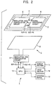
- Fig. 2 is a block diagram showing an IC card system which represents a first embodiment of the present invention.
- This IC card system 1 is applied to, for example, a ticket examination system for use in transport facilities.
- data is exchanged between an IC card 2 and a read/writer 3.
- the IC card 2 is formed into the shape of a card by laminating a protective sheet and a base plate on which integrated circuits are mounted.
- the IC card 2 has a loop antenna 4 formed of a wiring pattern on the base plate.
- a modulation and demodulation circuit 5 and a signal processing circuit 6 are formed by the integrated circuits formed on the base plate.
- the loop antenna 4 is coupled to a loop antenna 8 of the read/writer 3.
- the loop antenna 4 receives a transmission signal sent from the loop antenna 8 and radiates a response signal formed by the modulation and demodulation circuit 5.
- the modulation and demodulation circuit 5 produces necessary electric power, a clock signal, etc., for the operation of the IC card 2 from a transmission signal received by the loop antenna 4.
- the modulation and demodulation circuit 5 operates by the electric power and the clock signal to demodulate the received transmission signal to retrieve a data sequence sent from the read/writer 3 (hereinafter referred to as "transmitted data sequence") D (R ⁇ C).
- the modulation and demodulation circuit 5 outputs the data sequence to the signal processing circuit 6. By this transmitted data sequence, the modulation and demodulation circuit 5 is urged to transmit a response signal.
- the modulation and demodulation circuit 5 forms the response signal from a data sequence (hereinafter referred to as "response data sequence") D (C ⁇ R) input from the signal processing circuit 6 and radiates the response signal by driving the loop antenna 4 by the response signal.
- response data sequence a data sequence (hereinafter referred to as "response data sequence") D (C ⁇ R) input from the signal processing circuit 6 and radiates the response signal by driving the loop antenna 4 by the response signal.
- the signal processing circuit 6 operates by the electric power and the clock signal generated by the modulation and demodulation circuit 5 to analyze the transmitted data sequence D (R ⁇ C) and outputs a response data sequence D (C ⁇ R) to the modulation and demodulation circuit 5 by reading out this data sequence from an internal nonvolatile memory according to need.
- a modulation and demodulation circuit 9 receives a transmitted data sequence D (R ⁇ C) input from an signal processing unit (SPU) 10, and forms a transmission signal by modulating a carrier having a predetermined frequency in a binary phase shift keying (BPSK) or differential phase shift keying (DPSK) manner.
- BPSK binary phase shift keying
- DPSK differential phase shift keying
- any of various modulation methods such as ASK, PSK, Gaussian-filtered minimum shift keying (GMSK), frequency shift keying (FSK), and pulse modulation (PM), can be used according to need.
- the modulation and demodulation circuit 9 sends out the transmission signal from the loop antenna 8.
- the modulation and demodulation circuit 9 processes a response signal received by the loop antenna 8 to retrieve a response data sequence D (C ⁇ R) sent from the IC card 2 by demodulation and outputs this response data sequence D (C ⁇ R) to the SPU 10.
- the modulation and demodulation circuit 9 forms the transmission signal by a depth of modulation of about 10 %, such that, when electric fields formed by the loop antennas 4 and 8 are measured and the frequency spectrum thereof is observed, the power ratio of the carrier to the total power is equal to or higher than 99 %.
- the signal level of the carrier is thereby continuously maintained so as to be equal to or higher than a certain level when the transmission signal is received on the IC card 2 side. Simultaneously, the power of the sidebands is limited so as not to exceed a predetermined level.
- the SPU 10 is constituted of a calculation processing unit for executing a comparatively simple processing procedure.
- the SPU 10 sends to the modulation and demodulation circuit 9 a transmitted data sequence D (R ⁇ C) to be transmitted to the IC card 2.
- the SPU 10 also processes a response data sequence D (C ⁇ R) input from the modulation and demodulation circuit 9.
- the SPU 10 displays the progress and results of processing by a display section 11 according to need.
- the SPU 10 also changes the operation by a command from an input section 12 and exchanges data for a processing procedure, etc., with an external device 13 according to need.
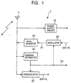
- Fig. 1 is a block diagram showing the modulation and demodulation circuit 5 of the IC card 2.
- a power supply circuit 19 receives a transmission signal induced in the loop antenna 4 and rectifies this transmission signal to generate power for operating the IC card 2.
- a carrier extractor 20 is formed of a phase locked loop (PLL) circuit which operates by limiting the amplitude of the transmission signal received by the loop antenna 4.
- the carrier extractor 20 generates a clock signal CK having the same frequency as the carrier of the transmission signal and phase-synchronized with the carrier.
- the carrier extractor 20 divides this clock signal to form operating clock signals for the signal processing circuit 6 and to other components. Even if the power of the transmission signal received by the loop antenna 4 varies largely, the carrier extractor 20 generates, at a constant level, the clock signal CK having the same frequency as the carrier of the transmission signal and phase-synchronized with the carrier.
- a demodulator 22 receives the transmission signal from the loop antenna 4 and processes and demodulates the transmission signal by using the clock signal CK output from the carrier extractor 20, thereby retrieving the transmitted data sequence D (R ⁇ C) transmitted by the transmission signal.
- the demodulator 22 outputs the transmitted data sequence D (R ⁇ C) to the signal processing circuit 6.
- a modulator 23 is formed of a PSK modulator, and modulates the clock signal CK output from the carrier extractor 20 with the response data sequence D (C ⁇ R) to form a PSK-modulated signal S1.
- a level adjuster 24 corrects the signal level of the PSK-modulated signal S1 to a predetermined signal level to form a response signal, and outputs the response signal to the loop antenna 4.
- the level adjuster 24 observes the signal level on the connection line to the loop antenna 4, and corrects the signal level of the modulated signal S1 so that the carrier observed on the line is maintained at a signal level equal to or higher than a certain value even if the logical level of the response data sequence D (C ⁇ R) varies, thereby enabling the carrier extractor 20 formed of a PLL circuit to operate stably.
- the carrier is modulated with the transmitted data sequence D (R ⁇ C) to be sent from the read/writer 3 to the IC card 2, and the modulated signal is sent out from the loop antenna 8.
- the IC card 2 When the IC card 2 is brought close to the read/writer 3 operating in this manner, the corresponding transmission signal is induced in the loop antenna 4 of the IC card 2. A portion of this induced transmission signal is converted into electric power for the IC card 2 by the power supply circuit 19. The modulation and demodulation circuit 5 and the signal processing circuit 6 and other components of the IC card 2 are driven by this electric power.
- the transmitted data sequence D (R ⁇ C) is reproduced by the demodulator 22.
- the transmitted data sequence D (R ⁇ C) is then analyzed in the signal processing circuit 6 to form the response data sequence D (C ⁇ R) to be sent to the read/writer 3.
- the response data sequence D (C ⁇ R) is input to the modulator 23.
- the clock signal CK output from the carrier extractor 20 is modulated with the response data sequence D (C ⁇ R) to obtain PSK-modulated signal S1.
- the level of PSK-modulated signal S1 is corrected to a constant signal level by the level adjuster 24 and is thereafter output to the loop antenna 4.
- the PSK-modulated signal S1 Since the clock signal CK output from the carrier extractor 20 has the same frequency as the carrier of the transmission signal and phase-synchronized with the carrier, the PSK-modulated signal S1 has the same frequency as the carrier of the transmission signal and has its phase changed in accordance with the response data sequence D (C ⁇ R). As the phase change in the response signal radiated from the loop antenna 4, the response data sequence D (C ⁇ R) is transmitted.
- Data exchange can be reliably performed by these means without using a semiconductor device having a sufficiently high withstand voltage to change the load impedance of the antenna as in the conventional load switching system.
- clock signal CK maintained at a constant signal level is produced by the carrier extractor 20, and the modulated signal S1 is formed from this clock signal CK to transmit the response data sequence D (C ⁇ R), thereby sending out the response signal from the loop antenna 4 by constant power.
- response signal is sent out by constant power from the loop antenna and the need for a means for coping with such an excessively large input can be eliminated.
- the configuration of the read/writer 3 can be correspondingly simplified.
- clock signal CK having the same frequency as the main carrier of the transmission signal sent from the read/writer 3 and phase-synchronized with the carrier is generated, and PSK-modulated signal S1 formed from this clock signal CK is sent out from the loop antenna 4.
- the desired data exchange can be performed by a system arranged as simply as the load switching system without using a semiconductor device having a sufficiently high withstand voltage.
- the circuit components forming the IC card 2 can easily by combined into an integrated circuit. Also, damage to the IC card when a high voltage is applied to the IC card by static electricity or the like can be reduced in comparison with the conventional art.
- the response signal can be sent out from the loop antenna 4 by constant power. Therefore, the need for a means for coping with an excessively large input on the read/writer 3 side can be eliminated and the configuration of the read/writer 3 can be simplified.
- the method of forming the clock signal by limiting the amplitude of the input signal in the carrier extractor 20 also enables stable generation of clock signal CK while the power of the transmission signal induced in the loop antenna 4 is changed. Also, damage to the carrier extractor 20 can be reliably avoided thereby.
- the depth of modulation is set to 10 %, so that the carrier can be continuously monitored in the response signal received by the loop antenna 4.
- the clock signal can be produced with stability in the carrier extractor 20 arranged as a PLL circuit, thereby making it possible to stably exchange data and to stably supply electric power from the power supply circuit 19.
- the ratio of the carrier power to the total power in the transmission signal is set to 99 % or higher, thereby effectively reducing parasitic emissions.
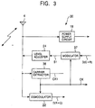
- Fig. 3 is a block diagram showing a modulation and demodulation circuit 30 of an IC card used in an IC card system which represents a second embodiment of the present invention.
- the same components as those described above with reference to Fig. 1 are indicated by the same reference numerals and the description for them will not be repeated.
- modulated signal S1 is formed by switching a clock signal CK having the same frequency as a carrier and phase-synchronized with the carrier and a clock signal CKI formed by inverting the signal level of the clock signal CK.
- a carrier extractor 36 forms clock signal CK from the output from the loop antenna 4 and outputs the clock signal CK.
- the carrier extractor 36 also forms and outputs clock signal CKI having a phase difference of 180° from the clock signal CK by forming an inverted signal of clock signal CK.
- a modulator 37 is formed by a switching circuit which selects and outputs clock signal CK or CKI according to response data sequence D (C ⁇ R). The modulator 37 thereby outputs a PSK-modulated signal the phase of which is changed according to response data sequence D (C ⁇ R).
- modulated signal S1 is output to the loop antenna 4 after the signal level of modulated signal S1 has been corrected by the level adjuster 24.
- the signal level of the carrier is thereby enhanced or lowered at the input terminal of the loop antenna according to response data sequence D (C ⁇ R), and PSK-modulated signal S1 thus formed is sent out.
- modulated signal is formed by switching the clock signal CK having the same frequency as the carrier and phase-synchronized with the carrier and the clock signal CKI having a phase difference of 180° from the clock signal CK, so that the configuration of the modulator 37 for modulating response data sequence D (C ⁇ R) can be simplified while the same advantages as those of the first embodiments are achieved.
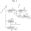
- Fig. 4 is a block diagram showing a modulation and demodulation circuit 40 of an IC card used in an IC card system which represents a third embodiment of the present invention.
- the load impedance of the loop antenna 4 is changed by changing the power supply load.
- the same components as those described above with reference to Fig. 1 are indicated by the same reference numerals and the description for them will not be repeated.
- a rectification circuit 41 rectifies a response signal output from the loop antenna 4 to produce electric power for the IC card 2.
- a stabilization circuit 42 stabilizes the output voltage of the rectification circuit 41 and supplies the stabilized output to the signal processing circuit, the demodulator 22 and other components.
- a level adjuster 43 corrects the signal level of response data sequence D (C ⁇ R) to a predetermined signal level and outputs the corrected signal.
- a bandpass filter (BPF) 44 performs band limitation of the output signal of the level adjuster 43 and then outputs the signal to the output terminal of the rectification circuit 41 through a capacitor 45.
- the level adjuster 43 and the bandpass filter 44 thereby change the power supply load according to the logical level of response data sequence D (C ⁇ R).
- the load impedance of the loop antenna 4 is thereby changed to send out the response signal.
- the power supply load is changed according to the logical level of response data sequence D (C ⁇ R), so that data exchange can be performed by a system arranged as simply as the load switching system without using a semiconductor device having a particularly high withstand voltage for sending out response data D (C ⁇ R).
- the circuit components forming the IC card 2 can easily by combined into an integrated circuit. Also, damage to the IC card when a high voltage is applied to the IC card by static electricity or the like can be reduced in comparison with the conventional art.
- the power supply voltage output from the rectification circuit 41 has superposed pulsating components of the carrier.
- the signal level of the pulsating components increases.
- such pulsating components are suppressed by the capacitor 45 and the bandpass filter 44, so that application of an excessively high voltage to the output terminal of the level adjuster 43 can be reliably avoided.
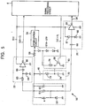
- Fig. 5 is a block diagram showing a modulation and demodulation circuit 50 of an IC card used in an IC card system which represents a fourth embodiment of the present invention.
- the same components as those described above with reference to Fig. 4 are indicated by the same reference numerals and the description for them will not be repeated.
- the read/writer forms a transmission signal by ASK modulation and sends out the formed signal.
- a capacitor 51 is connected in parallel with loop antenna 4.
- the loop antenna 4 and the capacitor 51 form a parallel resonance circuit for resonance with a carrier.
- the loop antenna 4 is thus arranged to receive a transmission signal selectively and efficiently and to radiate a response signal efficiently.
- a diode 52 having its cathode grounded is connected to one terminal of the loop antenna 4, and the other terminal of the loop antenna 4 is grounded by a capacitor 53.
- the loop antenna 4 is maintained by a rectification circuit formed of the diode 52 and the capacitor 53 as a detection circuit at a dc level obtained by rectifying the carrier.
- the terminal voltage of the loop antenna 4 maintained in this manner is changed according to a transmission signal and a response signal.
- a stabilization circuit 54 is supplied with the terminal voltage of the loop antenna 4 via a resistor 56, and produces power for operating the IC card 2 from the power of a transmission signal received by the loop antenna 4. At this time, the stabilization circuit 54 grounds the power input by a clamp circuit formed by series connection of six diodes 57A to 57F, thereby reliably avoiding damage caused by an excessively large input voltage.
- a carrier extractor 20 removes the dc component from the terminal voltage of the loop antenna 4 by a capacitor 58, performs binary recognition in reference to the zero level with a comparison circuit 59 operating by operating power supply VCC, and thereby produces clock signal CK having the same frequency as the carrier and phase-synchronized with the carrier.
- the carrier extractor 20 also has an amplitude limitation circuit formed of diodes 61 and 60 connected to the input terminal to reliably avoid an excessively large amplitude input.
- a demodulator 22 performs band limitation of the terminal voltage of the loop antenna 4 with a low-pass filter formed of a resistor 63 and a capacitor 64, then removes the dc component with a capacitor 65, and inputs the voltage to a comparison circuit 66.
- the comparison circuit 66 operates by operating power supply VCC and performs binary recognition of the input voltage in reference to the zero level.
- the demodulator 22 obtains and outputs transmitted data sequence D (R ⁇ C) by this demodulation.
- an excessively large amplitude input to the comparison circuit 66 is reliably avoided by inputting the terminal voltage of the loop antenna to the comparator 66 after band limitation has been performed by the low-pass filter formed of resistor 63 and capacitor 64 and after the dc component has been removed by capacitor 65.
- a level adjuster 43 is formed of a FET 69 which forms a switching circuit and which operates by response data sequence D (C ⁇ R), and a resistor 70 for supplying power to the FET 69.
- the level adjuster 43 corrects the signal level of response data sequence D (C ⁇ R) to the signal level determined by the terminal voltage of the resistor 70, and outputs the corrected signal.
- the resistor 70 is connected to the anode of the diode 57A closest to the resistor 56 in the group of diodes 57A to 57F forming the clamp circuit to supply power, thereby correcting the signal level of response data sequence D (C ⁇ R) to the signal level determined by the other diodes 57B to 57F and outputting the corrected response data sequence D (C ⁇ R).
- a low-pass filter 72 is formed of a resistor 73 and a capacitor 74.
- the low-pass filter 72 performs band limitation of the output signal from the level adjuster 43 and then outputs the signal to one terminal of the loop antenna 4 via a capacitor 45.
- the same advantages as those of the third embodiment can also be achieved by performing band limitation of the output signal from the level adjuster 43 through the low-pass filter 72.
- the carrier extractor may alternatively be formed by a comparison circuit.
- the carrier extractor may alternatively be formed by a PLL circuit.
- the embodiments have been described with respect to the case where a transmission signal is formed by modulation to a depth of 10 %, but the present invention is not limited to this. If the power of the sidebands is not restricted by law, or in a like situation, the transmission signal may be formed by a depth of modulation smaller than 1 to achieve the same advantages as the above-described embodiments.
- the embodiments have been described with respect to the case where the reference signal is sent out by being PSK-modulated, but the present invention is not limited to this.
- the reference signal may be sent out by being modulated by an ASK modulation method such that it is selectively sent out from the antenna according to the response data sequence.
- the present invention can find various applications in which the frequency of main carrier is set to, for example, 13.56 MHz, a frequency in a microwave band or any other frequencies.
- an IC card capable of performing data exchange without a semiconductor device having a sufficiently large withstand voltage while being arranged as simply as the load switching system, and an IC card system using the an IC card can be obtained.
- This performance can be achieved by forming a reference signal having the same frequency as a carrier of a transmission signal and phase-synchronized with the carrier and forming a response signal by modulating the reference signal, or changing the load on the power supply circuit according to the response data sequence.
Landscapes
- Engineering & Computer Science (AREA)
- Physics & Mathematics (AREA)
- General Physics & Mathematics (AREA)
- Theoretical Computer Science (AREA)
- Artificial Intelligence (AREA)
- Computer Vision & Pattern Recognition (AREA)
- Computer Networks & Wireless Communication (AREA)
- Computer Hardware Design (AREA)
- Microelectronics & Electronic Packaging (AREA)
- Near-Field Transmission Systems (AREA)
- Radar Systems Or Details Thereof (AREA)
Applications Claiming Priority (2)
| Application Number | Priority Date | Filing Date | Title |
|---|---|---|---|
| JP2829398 | 1998-02-10 | ||
| JP10028293A JPH11234163A (ja) | 1998-02-10 | 1998-02-10 | Icカード及びicカードシステム |
Publications (2)
| Publication Number | Publication Date |
|---|---|
| EP0936574A2 true EP0936574A2 (de) | 1999-08-18 |
| EP0936574A3 EP0936574A3 (de) | 2000-05-17 |
Family
ID=12244581
Family Applications (1)
| Application Number | Title | Priority Date | Filing Date |
|---|---|---|---|
| EP99102543A Withdrawn EP0936574A3 (de) | 1998-02-10 | 1999-02-10 | Ic-Karte und Ic-Kartensystem |
Country Status (5)
| Country | Link |
|---|---|
| US (1) | US6193164B1 (de) |
| EP (1) | EP0936574A3 (de) |
| JP (1) | JPH11234163A (de) |
| AU (1) | AU763002B2 (de) |
| SG (1) | SG85104A1 (de) |
Cited By (1)
| Publication number | Priority date | Publication date | Assignee | Title |
|---|---|---|---|---|
| EP1986136A1 (de) | 2007-04-26 | 2008-10-29 | EM Microelectronic-Marin SA | Transponderschaltung mit doppelter Taktableitungseinheit |
Families Citing this family (12)
| Publication number | Priority date | Publication date | Assignee | Title |
|---|---|---|---|---|
| JP3922501B2 (ja) * | 1998-12-10 | 2007-05-30 | ソニー株式会社 | 電源装置及びカード状記憶媒体 |
| ES2381940T3 (es) * | 2000-07-26 | 2012-06-01 | Bridgestone Americas Tire Operations, Llc | Sistema electrónico de gestión de neumáticos |
| JP2003085506A (ja) * | 2001-09-12 | 2003-03-20 | Yoshikawa Rf System Kk | データキャリアにおける過電圧防止回路 |
| JP2006277178A (ja) * | 2005-03-29 | 2006-10-12 | Aruze Corp | ゲーム用カード |
| JP2006271596A (ja) * | 2005-03-29 | 2006-10-12 | Aruze Corp | ゲーム用カード |
| US20080143192A1 (en) * | 2006-12-14 | 2008-06-19 | Sample Alanson P | Dynamic radio frequency power harvesting |
| JP2008246104A (ja) * | 2007-03-30 | 2008-10-16 | Angel Shoji Kk | Rfidを内蔵したゲームカードおよびその製造方法 |
| JP5155642B2 (ja) * | 2007-11-28 | 2013-03-06 | ルネサスエレクトロニクス株式会社 | Idタグ |
| FR2931601B1 (fr) * | 2008-05-26 | 2010-04-23 | Commissariat Energie Atomique | Dispositif, systeme et procede de communication radiofrequence |
| DE102009052936B8 (de) | 2009-11-12 | 2012-05-10 | Andrew Wireless Systems Gmbh | Master-Einheit, Remote-Einheit sowie Multiband-Übertragungssystem |
| US10237000B1 (en) * | 2018-05-08 | 2019-03-19 | Nxp B.V. | Phase compensation in an NFC system |
| CN110176266B (zh) * | 2019-05-30 | 2021-03-02 | 苏州汇成芯通物联网科技有限公司 | 超高频射频芯片的nvm快速编码系统 |
Family Cites Families (7)
| Publication number | Priority date | Publication date | Assignee | Title |
|---|---|---|---|---|
| US4546241A (en) | 1982-12-10 | 1985-10-08 | Walton Charles A | Electronic proximity identification system |
| GB8408538D0 (en) | 1984-04-03 | 1984-05-16 | Senelco Ltd | Transmitter-responder systems |
| JP2612190B2 (ja) | 1988-08-31 | 1997-05-21 | 山武ハネウエル株式会社 | 応答装置と質問装置からなる全二重通信装置 |
| FR2648593B1 (fr) | 1989-06-14 | 1992-08-21 | Raimbault Pierre | Procede et dispositif de comptabilisation et de controle d'articles |
| US5418353A (en) | 1991-07-23 | 1995-05-23 | Hitachi Maxell, Ltd. | Non-contact, electromagnetically coupled transmission and receiving system for IC cards |
| US5517194A (en) | 1994-02-10 | 1996-05-14 | Racom Systems, Inc. | Passive RF transponder and method |
| JPH07264091A (ja) | 1994-03-18 | 1995-10-13 | Toshiba Corp | 無線カード用通信装置 |
-
1998
- 1998-02-10 JP JP10028293A patent/JPH11234163A/ja active Pending
-
1999
- 1999-02-02 US US09/243,671 patent/US6193164B1/en not_active Expired - Fee Related
- 1999-02-03 AU AU14711/99A patent/AU763002B2/en not_active Ceased
- 1999-02-04 SG SG9900369A patent/SG85104A1/en unknown
- 1999-02-10 EP EP99102543A patent/EP0936574A3/de not_active Withdrawn
Cited By (2)
| Publication number | Priority date | Publication date | Assignee | Title |
|---|---|---|---|---|
| EP1986136A1 (de) | 2007-04-26 | 2008-10-29 | EM Microelectronic-Marin SA | Transponderschaltung mit doppelter Taktableitungseinheit |
| US8195100B2 (en) | 2007-04-26 | 2012-06-05 | Em Microelectronic-Marin Sa | Transponder circuit with double clock extractor unit |
Also Published As
| Publication number | Publication date |
|---|---|
| AU763002B2 (en) | 2003-07-10 |
| AU1471199A (en) | 1999-08-26 |
| EP0936574A3 (de) | 2000-05-17 |
| SG85104A1 (en) | 2001-12-19 |
| US6193164B1 (en) | 2001-02-27 |
| JPH11234163A (ja) | 1999-08-27 |
Similar Documents
| Publication | Publication Date | Title |
|---|---|---|
| US5889273A (en) | Wireless communication data storing medium for receiving a plurality of carriers of proximate frequencies and a transmission/receiving method | |
| CA1336724C (en) | Full duplex transponder system | |
| US6193164B1 (en) | IC card and IC card system | |
| US6507607B1 (en) | Apparatus and method for recovering a clock signal for use in a portable data carrier | |
| De Vita et al. | Design criteria for the RF section of UHF and microwave passive RFID transponders | |
| US8797163B2 (en) | Transponder unit | |
| EP2057589B1 (de) | Etikette, leser und rfid system | |
| US5847662A (en) | Radio card communication apparatus | |
| US7221908B2 (en) | Radio communication apparatus | |
| EP0936571A2 (de) | Chipkarte und ihr Verarbeiter und System | |
| US7177621B2 (en) | Wireless communication medium and method for operating the same | |
| CN103714375A (zh) | 有源标签及其射频前端芯片 | |
| US10103782B2 (en) | Method for detecting the eventual presence of an object by a contactless reader, and corresponding reader | |
| US8183981B2 (en) | Passive tag with oscillator circuit and frequency identification system utilizing the same | |
| WO2020052285A1 (zh) | 一种射频识别电路及非接触式ic卡防盗器 | |
| JP2006180491A (ja) | 自律電源供給のない電磁トランスポンダ | |
| JP4123483B2 (ja) | 通信システム、通信方法、データ処理装置、およびデータ処理方法 | |
| JP4560744B2 (ja) | 通信システム、通信方法、データ処理装置、およびデータ処理方法 | |
| JPH11266176A (ja) | 受動型トランスポンダ装置およびその動作方法 | |
| JP2000259788A (ja) | 非接触icカードシステムおよび非接触icカードの外部読み書き装置 | |
| EP1415264B1 (de) | Lesegerät für berührungslose chipkarten, wobei entlang einer übertragungsleitung von der antenne zum empfänger die modulierung wechselt zwischen amplituden- und phasenmodulation | |
| JP2000151458A (ja) | 電磁誘導型トランスポンダ方式 | |
| JPH09161029A (ja) | 非接触icカードのデータアクセス装置 | |
| JPH0969144A (ja) | Icカードおよびicカードのアクセス装置/アクセス方法 | |
| WO2009113015A2 (en) | Data processing system |
Legal Events
| Date | Code | Title | Description |
|---|---|---|---|
| PUAI | Public reference made under article 153(3) epc to a published international application that has entered the european phase |
Free format text: ORIGINAL CODE: 0009012 |
|
| AK | Designated contracting states |
Kind code of ref document: A2 Designated state(s): DE FR GB IT |
|
| AX | Request for extension of the european patent |
Free format text: AL;LT;LV;MK;RO;SI |
|
| PUAL | Search report despatched |
Free format text: ORIGINAL CODE: 0009013 |
|
| AK | Designated contracting states |
Kind code of ref document: A3 Designated state(s): AT BE CH CY DE DK ES FI FR GB GR IE IT LI LU MC NL PT SE |
|
| AX | Request for extension of the european patent |
Free format text: AL;LT;LV;MK;RO;SI |
|
| 17P | Request for examination filed |
Effective date: 20001116 |
|
| AKX | Designation fees paid |
Free format text: DE FR GB IT |
|
| STAA | Information on the status of an ep patent application or granted ep patent |
Free format text: STATUS: THE APPLICATION HAS BEEN WITHDRAWN |
|
| 18W | Application withdrawn |
Withdrawal date: 20021004 |