EP0938048A1 - Verfahren zur seriellen Datenübertragung und synchrone und serielle Busschnittstelle zur Durchführung dieses Verfahrens - Google Patents
Verfahren zur seriellen Datenübertragung und synchrone und serielle Busschnittstelle zur Durchführung dieses Verfahrens Download PDFInfo
- Publication number
- EP0938048A1 EP0938048A1 EP99400345A EP99400345A EP0938048A1 EP 0938048 A1 EP0938048 A1 EP 0938048A1 EP 99400345 A EP99400345 A EP 99400345A EP 99400345 A EP99400345 A EP 99400345A EP 0938048 A1 EP0938048 A1 EP 0938048A1
- Authority
- EP
- European Patent Office
- Prior art keywords
- cycle
- transfer
- address
- shift register
- read
- Prior art date
- Legal status (The legal status is an assumption and is not a legal conclusion. Google has not performed a legal analysis and makes no representation as to the accuracy of the status listed.)
- Granted
Links
Images




Classifications
-
- G—PHYSICS
- G06—COMPUTING OR CALCULATING; COUNTING
- G06F—ELECTRIC DIGITAL DATA PROCESSING
- G06F13/00—Interconnection of, or transfer of information or other signals between, memories, input/output devices or central processing units
- G06F13/38—Information transfer, e.g. on bus
- G06F13/42—Bus transfer protocol, e.g. handshake; Synchronisation
- G06F13/4282—Bus transfer protocol, e.g. handshake; Synchronisation on a serial bus, e.g. I2C bus, SPI bus
- G06F13/4291—Bus transfer protocol, e.g. handshake; Synchronisation on a serial bus, e.g. I2C bus, SPI bus using a clocked protocol
Definitions
- the present invention relates to the field of transmission of serial digital data. It relates more particularly to a bus synchronous and its transmission protocol in master / slave mode between a main unit (master) and a peripheral unit (slave).
- I 2 C bus An example of such a bus, used in various categories of device, is the so-called I 2 C bus described in European patent 0 051 332.
- a number of clock cycles are necessary for the microprocessor or microcontroller constituting the unit. main to recover a byte of data (58 clock cycles in the case of the circuit marketed by the company PHILIPS under the reference PCD 3316 using such a bus).
- An object of the present invention is to propose a new synchronous serial bus protocol for faster access to some data in the peripheral unit.
- the transfer protocol is very simple, so that it allows quick access. It is based on the detection of the activation pulse, or "strobe", on the data line by the peripheral unit. The main unit distinguishes the different transfer modes by the position of this pulse activation during the cycle and / or by means of selection bits presented on the data line before the activation pulse and / or by decoding address bits.
- Very fast access to certain memory locations of the peripheral unit is made possible by the direct transfer mode, being since the main unit does not have address bits in this mode, and that the desired information is selected beforehand.
- the location where the transmitted data bits are obtained in direct transfer mode can be a predetermined fixed location, which simplifies the structure of the unit's bus interface as much as possible device and therefore minimize its cost.
- It can also be a location whose address is obtained from information supplied by the main unit during a cycle of previous writing.
- direct read cycles can be executed by the main unit to read different types of information in the peripheral unit.
- the number of bits thus read can also be a parameter set by the main unit during an earlier write cycle.
- the direct reading mode can in particular be used in the rapid handling of certain interruptions by the main unit.
- Another advantage of the proposed bus is that it can share its line data and its clock line with those of a bus operating on a other protocol for data exchange between the main unit and others entities.
- Figure 1 schematically shows an apparatus whose general operation is controlled by a main unit constituted by a microprocessor 10.
- the microprocessor 10 supervises a certain number of units (not shown) of the apparatus via a serial bus 11 of known type, such as for example an I 2 C bus comprising an SDA data line and a SCL clock line (see EP-B-0 051 332).
- Another peripheral unit 12 is supervised by the microprocessor 10 using a serial bus 13 operating in accordance with the invention.
- the device can be a telephone set, the microprocessor 10 of which supervises, using the I 2 C bus 11, units such as a keyboard, a display screen and various interfaces, unit 12 is a component dedicated to the observation of the telephone line and the processing of certain data relating to advanced services offered by network operators.
- the cost of the components must be the as low as possible, and it is particularly desirable to be able to limit as much as possible the number of input / output pins of the microprocessor.
- the bus 13 used for exchanges between units 10 and 12 uses the general bus 11 data and clock lines, which are also noted BDA and BCL. The protocol which will be described below avoids ambiguities on these lines.
- Bus 13 also includes an INT interrupt line allowing the peripheral unit 12 to report certain events to the microprocessor 10 by sending a request for interruption.
- the bus interface provided between the operational circuits 15 of the peripheral unit 12 and the bus 13, comprises an input / output module 16 and a module 17 for processing interruptions.
- the module 17 receives from the circuits 15 respective interrupt signals IRQ 1 -IRQ n relating to a set of n events whose detection triggers the sending on the line INT of an interrupt request.
- the module 17 manages the storage, in a state register of the module 16, of n bits corresponding to the states of the signals IRQ 1 -IRQ n .
- the microprocessor 10 reads the status register in order to know the origin of the interrupt and to determine the interrupt program to be executed.
- the set of events associated with the interrupt signals IRQ 1 -IRQ n includes for example the detection of a ring on the line, the detection of the presence of the voltage and the detection of various signals that the network transmits over the telephone line as part of specific services.
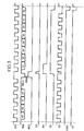
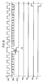
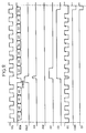
- the first two lines of Figures 2 to 4 show how the microprocessor 10 controls the BCL, BDA lines of bus 13 to trigger data transfers from or to the peripheral unit 12.
- the use of bus 13 is signaled by an activation pulse (strobe) presented during a transfer cycle on the BDA data line while the BCL clock line is at a given logic level.
- this logical level is level 1
- m 4 bits A3-A0 form an address write for storing the previous byte.
- the pulse activation is preceded by m + 1 synchronization pulses on the line BCL clock, m + 1 bits being transmitted as before by the microprocessor on the BDA data line.
- the activation pulse is transmitted by the microprocessor at the start of the cycle.
- the clock frequency being 500 kHz
- microprocessor 10 When it is not performing a transfer cycle on the bus 11/13, microprocessor 10 maintains the SDA / BDA clock line at logic level 1.
- the structure of the input / output module 16 of the peripheral unit 12 is for example in accordance with the diagram in FIG. 5.
- the reference 18 designates a grouping of M 2 2 m registers of n bits in which the microprocessor 10 can order writes in cycles such as that shown in FIG. 2, the grouping register 18 where such writting takes place being chosen using the write address A3-A0.
- the reference 19 designates a grouping of M ⁇ 2 m registers of n bits in which the microprocessor 10 can control data readings in reading cycles with addressing such as that represented in FIG. 3, the register of the grouping 19 where a such reading takes place being chosen using the reading address A3-A0.
- These read registers 19 include the state register used for managing the interrupts.
- the module 16 includes a shift register consisting of m + 1 flip-flops D in cascade 20 0 -20 m clocked by the rising edges of the signal present on the clock line BCL.
- the data input of this shift register that is to say the input D of the first flip-flop 20 0 , is connected to the data line BDA.
- the module 16 includes a second shift register consisting of n flip-flops D in cascade 20 m + 1 -20 m + n clocked by the rising edges of a DC signal delivered by an EXCLUSIVE OR gate 21.
- the input D of the flip-flop 20 i is connected to the output Q of the flip - flop 20 i-1 .
- Gate 21 has an input connected to the clock line BCL. Its other input receives a binary selection signal CD.
- the mode selection bit RW is present at the output Q of the flip-flop 20 0
- the m address bits A3-A0 are present at the outputs Q of the flip-flops 20 1 -20 m .
- An auxiliary register of m bits consists of m flip-flops D 22 1 -22 m .
- the input D of the flip-flop 22 i is connected to the output Q of the flip-flop 20 i .
- the outputs Q of the flip-flops 22 1 -22 m supply the m address bits delivered to the group of write registers 18 and to the group of read registers 19. So that this auxiliary register 22 1 -22 m receives the address A3 -A0 at the moment of detection of the activation pulse in a write or read cycle with addressing, flip-flops D 22 1 -22 m are clocked by the rising edges of a HOLD signal delivered by a detector d activation pulses 24.
- This detector 24 (FIG. 6) comprises two flip-flops D 25,26 of which the Q outputs are reset to logic level 0 on each falling edge occurring on the BCL clock line.
- the BCL line is connected to input D of the flip-flop 25 which is clocked by the falling edges occurring on the line BDA data, and whose Q output delivers the aforementioned HOLD signal.
- This signal is also addressed to the input D of the flip-flop 26 clocked by the fronts amounts occurring on the BDA data line, and whose Q output delivers a STRI detection signal.
- This STRI signal has a level pulse logic 1 which begins at the end of each activation pulse and ends when the BCL line returns to 0.
- An AND gate 28 combines the signal STRI with the logical complement of the bit RW obtained on the output Q of the flip-flop 20 0 to produce the write command signal WR addressed to the group of write registers 18.
- This signal WR (FIG. 2) controls the transfer in parallel of the n bits D7-D0 present on the outputs Q of the flip-flops 20 m + i -20 m + n in the register of the group 18 whose location is designated by the m address bits A3- A0 obtained on the outputs Q of flip-flops 22 1 -22 m .
- Another AND gate 29 receives the signal STRI and the selection bit RW obtained on the output Q of the flip-flop 20 0 to produce a signal RR having the same appearance in the read cycles (FIGS. 3 and 4).
- microprocessor 10 For reading cycles with addressing and direct read cycles, it is expected that a value of the address of reading is excluded by microprocessor 10 for reading cycles with addressing. As an example, this can be the value for which all the bits are at 1.
- This signal F has a falling edge at the end of each transfer cycle I 2 C, as shown in the left part of FIG. 4.
- This signal F is for example supplied by the inverting output Q of a D flip-flop 27 of the activation pulse detector 24 (FIG. 6).
- This flip-flop 27 is reset to level 0 at each falling edge occurring on the clock line BCL.
- the line BCL is connected to the input D of the flip-flop 27 which is clocked by the rising edges occurring on the data line BDA.
- the CP preset signal is formatted such that the microprocessor 10 can decide at any time to execute a cycle of direct reading.
- the AND gates 28, 29 are supplemented by a detection logic 33 connected to the outputs Q of the flip-flops of the auxiliary register 22 1 -22 m .
- This detection logic 33 which consists simply of an AND gate with m inputs in the case where the excluded address value is 11 ... 1, delivers a selection bit FRM which is at 1 when the excluded address is detected and 0 otherwise.
- the means 30 for managing the read cycles include in in addition to an address switch 34 controlled by the FRM bit, a module for timing 35 and an address management module 36.
- the module 35 delivers the read command signal RD supplied to the group of registers 19. This signal RD is produced in response to the pulse of the signal RR delivered by the gate AND 29, and corresponds to this prolonged pulse during a cycle of BCL clock, as shown in Figures 3 and 4.
- a three-state door 40 forms an output switch of the input / output module 16, with its input connected to the output Q of the last flip-flop 20 m + n of the second shift register, and its output connected to the line of BDA data.
- the parameters p (number of bits transferred in a direct read cycle), a (start address) and ⁇ (possible offset) can be fixed, as in the example previously described. They can also be parameters programmable by the microprocessor 10. In this case, the modules 35, 36 and 38, which use these parameters p , a and respectivement respectively, obtain them from one of the writing registers of the grouping. 18. To modify any of these parameters, the microprocessor 10 can simply execute a write cycle in the register or registers in question, whose addresses it knows.
- the direct transfer cycles are not limited to read cycles. Direct write cycles are also possible.
- the mode selection bit RW is not transmitted by the microprocessor. The distinction between the read cycles and the write cycles is made on the basis of a decoding of the addresses present in the auxiliary register 22 1 -22 m when the activation pulse is detected.
- the input-output module shown in Figure 7 has many common elements with that of Figure 5, which are designated by the same reference numerals.
- the first shift register the input of which is connected to the data line BDA of the bus 13, has one less flip-flop since the bit RW no longer needs to be taken into account.
- the scales 20 1 -20 m remain and are coupled in the same way to the scales 22 1 -22 m of the auxiliary register.
- the parallel output on m bits of the auxiliary register is connected to a logic for detecting the types of cycle 50, which also receives the STRI signal delivered by the activation pulse detector 24.
- the logic 50 operates a decoding of the addresses contained in the auxiliary register 22 1 -22 m when it receives a pulse from the STRI signal.
- This decoding obeys pre-established rules.
- these rules may consist in that (i) the addresses of the form 1 xx ... x (each x being 0 or 1) are used by the microprocessor in reading cycles with addressing, (ii) addresses of the form 0 xx ... x are used in write cycles with addressing, (iii) address 111 ...
- a decoding table (possibly programmable by the microprocessor 10) in the logic 50 more generally allows any combination of sizes of memory accessible in read and / or write.
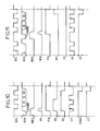
- logic 50 When a read cycle (direct or with addressing) is detected, logic 50 produces a logic level 1 pulse on the RR signal playing the same role as that described in the previous embodiment example (see Figures 9 and 10). When a write cycle (direct or with addressing) is detected, logic 50 similarly produces a level pulse logic 1 on the WW signal, as shown in Figures 8 and 11. In each direct transfer cycle, the logic 50 also activates an FM signal, playing a role similar to that of the FRM signal in the exemplary embodiment previous (it notably controls the address switch 34 which delivers address A for reading or writing, and possibly the module permutation 38).
- the detection logic 50 could still produce control signals C1, C2, ... in response to the detection of certain particular addresses in the auxiliary register 22 1 -22 m .
- This type of decoding optionally makes it possible to transmit commands to certain elements of the peripheral unit 12 without having to explicitly transfer data on the BDA line.
- FM, RR and WW signals delivered by the detection logic 50 are addressed to the transfer timing module 52 which is part of the means 30 for managing transfer cycles and playing a role similar to that of module 35 described with reference to FIG. 5.
- This module 52 produces the RD read and WR write control signals addressed to groupings of registers 19.18. Production of RD, CD and EORC signals by the module 52 is identical to that previously described ( Figures 9 and 10).
- the production of the write command signal WR takes account of the fact that, in the variant considered, the written data D7-D0 or d1-d0 are transmitted on the data line BDA by the microprocessor 10 after the activation pulse .
- the serial input of this register constituted by the input D of the flip-flop 20 m + 1 is directly connected to the BDA data line, as shown in FIG. 7.
- the input D of the flip-flop 20 m + 1 is connected either to the output Q of the flip-flop 20 m or else to the BDA data line according to the position of a switch.
- This switch could for example be controlled by a control bit C1 or C2 delivered by the detection logic 50 in response to a coded instruction from the microprocessor 10, which allows the microprocessor 10 to dynamically decide whether it transmits the data before or after the activation pulse in the write cycles.
- the microprocessor 10 presents a bit at 0 on the data line BDA at the same time as it executes a clock cycle on the line BCL just before transmitting the activation pulse in direct write cycles. This makes it possible to load a bit at 0 in flip-flops 20 1 and 22 1 in order to change the default address 111 ... 1 characterizing the direct reading cycles to the address 011 ... 1 characterizing the writing cycles direct, to allow adequate decoding by the detection logic 50.
- the control signal RD or WR is reactivated periodically as in previous example, and the address counter 36 is incremented by the output of an OR gate 54 receiving the signals RD and WR.
- the microprocessor can thus access several registers during the same direct transfer cycle.
Landscapes
- Engineering & Computer Science (AREA)
- Theoretical Computer Science (AREA)
- Physics & Mathematics (AREA)
- General Engineering & Computer Science (AREA)
- General Physics & Mathematics (AREA)
- Information Transfer Systems (AREA)
Applications Claiming Priority (2)
| Application Number | Priority Date | Filing Date | Title |
|---|---|---|---|
| FR9801831A FR2775091B1 (fr) | 1998-02-16 | 1998-02-16 | Procede de transfert de donnees en serie, et interface de bus serie synchrone mettant en oeuvre un tel procede |
| FR9801831 | 1998-02-16 |
Publications (2)
| Publication Number | Publication Date |
|---|---|
| EP0938048A1 true EP0938048A1 (de) | 1999-08-25 |
| EP0938048B1 EP0938048B1 (de) | 2004-08-18 |
Family
ID=9523002
Family Applications (1)
| Application Number | Title | Priority Date | Filing Date |
|---|---|---|---|
| EP99400345A Expired - Lifetime EP0938048B1 (de) | 1998-02-16 | 1999-02-12 | Verfahren zur seriellen Datenübertragung und synchrone und serielle Busschnittstelle zur Durchführung dieses Verfahrens |
Country Status (6)
| Country | Link |
|---|---|
| US (1) | US6182175B1 (de) |
| EP (1) | EP0938048B1 (de) |
| JP (1) | JPH11272609A (de) |
| CA (1) | CA2261840A1 (de) |
| DE (1) | DE69919426T2 (de) |
| FR (1) | FR2775091B1 (de) |
Cited By (1)
| Publication number | Priority date | Publication date | Assignee | Title |
|---|---|---|---|---|
| US9501446B2 (en) | 2010-05-27 | 2016-11-22 | Robert Bosch Gmbh | Control unit for the exchange of data with a peripheral unit, peripheral unit, and method for data exchange |
Families Citing this family (11)
| Publication number | Priority date | Publication date | Assignee | Title |
|---|---|---|---|---|
| TW468110B (en) * | 1998-05-04 | 2001-12-11 | Koninkl Philips Electronics Nv | Electronic apparatus with a bus |
| JP2005078523A (ja) * | 2003-09-02 | 2005-03-24 | Matsushita Electric Ind Co Ltd | シリアル転送装置 |
| DE102004057286A1 (de) * | 2004-11-26 | 2006-06-01 | Hasberg, Günter, Dr. | Elektronisches Steuerungssystem für die Automatisierungstechnik |
| US7869525B2 (en) * | 2005-08-01 | 2011-01-11 | Ati Technologies, Inc. | Dynamic bus inversion method and system |
| CN101300773A (zh) * | 2005-11-03 | 2008-11-05 | Nxp股份有限公司 | 数据接口及寻求同步的方法 |
| CN104350700B (zh) * | 2012-05-29 | 2017-05-31 | 飞思卡尔半导体公司 | 用于串行通信设备的时钟 |
| TW201418933A (zh) * | 2012-11-13 | 2014-05-16 | Accton Technology Corp | 時脈訊號之控制裝置及控制方法 |
| US20170017584A1 (en) * | 2015-07-15 | 2017-01-19 | Microchip Technology Incorporated | SPI Interface With Less-Than-8-Bit Bytes And Variable Packet Size |
| TW201915818A (zh) * | 2017-10-05 | 2019-04-16 | 香港商印芯科技股份有限公司 | 光學識別模組 |
| CN117708032B (zh) * | 2023-12-14 | 2024-10-25 | 苏州纳芯微电子股份有限公司 | 一种多通道同步并行i2c通信方法、系统、电子设备 |
| CN121077845A (zh) * | 2024-12-19 | 2025-12-05 | 北京中科腾越科技发展有限公司 | 两线串行移位通信协议实现方法及装置 |
Citations (3)
| Publication number | Priority date | Publication date | Assignee | Title |
|---|---|---|---|---|
| EP0159941A2 (de) * | 1984-04-10 | 1985-10-30 | Telemecanique | Serieller Verbindungsbus für Datenverabeitungssystem und Verfahren zum Informationsaustausch |
| EP0498494A1 (de) * | 1991-02-04 | 1992-08-12 | Koninklijke Philips Electronics N.V. | Datenkommunikationssystem auf einer Serienbusbasis und Uberwachungsstation zur Verwendung mit einem derartigen System |
| US5434862A (en) * | 1992-08-12 | 1995-07-18 | U.S. Philips Corporation | Multistation communication bus system, and a master station and a slave station for use in such system |
Family Cites Families (4)
| Publication number | Priority date | Publication date | Assignee | Title |
|---|---|---|---|---|
| NL8005976A (nl) | 1980-10-31 | 1982-05-17 | Philips Nv | Tweedraads-bussysteem met een kloklijndraad en een datalijndraad voor het onderling verbinden van een aantal stations. |
| US5671421A (en) * | 1994-12-07 | 1997-09-23 | Intel Corporation | Serial interrupt bus protocol |
| US5928345A (en) * | 1996-09-30 | 1999-07-27 | Rosemont Inc. | Field instrument with data bus communications protocol |
| US5758073A (en) * | 1996-12-02 | 1998-05-26 | Tritech Microelectronics International, Ltd. | Serial interface between DSP and analog front-end device |
-
1998
- 1998-02-16 FR FR9801831A patent/FR2775091B1/fr not_active Expired - Fee Related
-
1999
- 1999-02-12 DE DE69919426T patent/DE69919426T2/de not_active Expired - Fee Related
- 1999-02-12 US US09/249,147 patent/US6182175B1/en not_active Expired - Fee Related
- 1999-02-12 EP EP99400345A patent/EP0938048B1/de not_active Expired - Lifetime
- 1999-02-15 CA CA002261840A patent/CA2261840A1/en not_active Abandoned
- 1999-02-16 JP JP11037257A patent/JPH11272609A/ja active Pending
Patent Citations (3)
| Publication number | Priority date | Publication date | Assignee | Title |
|---|---|---|---|---|
| EP0159941A2 (de) * | 1984-04-10 | 1985-10-30 | Telemecanique | Serieller Verbindungsbus für Datenverabeitungssystem und Verfahren zum Informationsaustausch |
| EP0498494A1 (de) * | 1991-02-04 | 1992-08-12 | Koninklijke Philips Electronics N.V. | Datenkommunikationssystem auf einer Serienbusbasis und Uberwachungsstation zur Verwendung mit einem derartigen System |
| US5434862A (en) * | 1992-08-12 | 1995-07-18 | U.S. Philips Corporation | Multistation communication bus system, and a master station and a slave station for use in such system |
Cited By (1)
| Publication number | Priority date | Publication date | Assignee | Title |
|---|---|---|---|---|
| US9501446B2 (en) | 2010-05-27 | 2016-11-22 | Robert Bosch Gmbh | Control unit for the exchange of data with a peripheral unit, peripheral unit, and method for data exchange |
Also Published As
| Publication number | Publication date |
|---|---|
| CA2261840A1 (en) | 1999-08-16 |
| DE69919426D1 (de) | 2004-09-23 |
| EP0938048B1 (de) | 2004-08-18 |
| FR2775091B1 (fr) | 2000-04-28 |
| FR2775091A1 (fr) | 1999-08-20 |
| DE69919426T2 (de) | 2005-09-01 |
| JPH11272609A (ja) | 1999-10-08 |
| US6182175B1 (en) | 2001-01-30 |
Similar Documents
| Publication | Publication Date | Title |
|---|---|---|
| EP0938048B1 (de) | Verfahren zur seriellen Datenübertragung und synchrone und serielle Busschnittstelle zur Durchführung dieses Verfahrens | |
| EP0156724B1 (de) | Aufzeichnungsverfahren für einen Plattenspeicher und Plattenspeichersystem | |
| EP0113307B1 (de) | Anpassungseinrichtung für digitale Informationsblöcke fester Länge | |
| FR2827684A1 (fr) | Controleur de memoire presentant une capacite d'ecriture 1x/mx | |
| FR2594242A1 (fr) | Procede et appareil d'acces direct en memoire | |
| FR2471652A1 (fr) | Procede et systeme d'entree/sortie de donnees | |
| FR2528195A1 (fr) | Systeme de communication entre ordinateurs | |
| FR2513410A1 (fr) | Microprocesseur et procede pour imbriquer les acces en memoire de ce microprocesseur | |
| FR2503898A1 (fr) | Procede et dispositif d'allocation d'une ressource dans un systeme comportant des unites de traitement de donnees autonomes | |
| EP0635786B1 (de) | Einrichtung zur Speicherung von Daten | |
| EP1556766B1 (de) | Überwachung eines microprozessorprogramms durch das senden von zeitörtlichen nachrichten | |
| FR2686991A1 (fr) | Procede, systeme et processeur de communication entre une pluralite de sous-ensembles d'un equipement. | |
| WO2002052414A1 (fr) | Architecture electronique parallele comportant une pluralite d'unites de traitement connectees a un bus de communication, et adressables par leurs fonctionnalites | |
| EP1570356B1 (de) | Überwachungsvorrichtung mit einem optimierten pufferspeicher | |
| EP0557197B1 (de) | Zugriffszeitteilungssystem auf einen Speicher, der einem Prozessor und anderen Anwendungen gemeinsam ist | |
| FR2607648A1 (fr) | Procede et dispositif de transmission rapide de donnees entre un emetteur et un recepteur par liaison serie standard | |
| WO2003034246A2 (fr) | Dispositif de transmission de donnees asynchrones comprenant des moyens de controle de deviation d'horloge | |
| EP0655691B1 (de) | Prozessorschnittstellenschaltung zum Austausch von seriellen digitalen Daten mit einem Peripheriegerät | |
| EP0512882A1 (de) | Erkennungsverfahren und Steuerungsanordnung einer zu einem Empfänger gesendeten digitalen Nachrichtenform | |
| EP1554653B1 (de) | Übertragung von wiederholungsdigitalnachrichten zwischen einer überwachungsschaltung eines mikroprozessors und eines analysewerkzeugs | |
| FR2846822A1 (fr) | Reseau local industriel ou domestique | |
| FR2582423A1 (fr) | Memoire tampon a interposer entre deux systemes synchrones a vitesses differentes | |
| EP1576476A1 (de) | Überwachungschaltung eines mikroprozessors und analysewerkzeug und seine ein- und ausgänge | |
| FR2767590A1 (fr) | Dispositif d'enregistrement de messages numeriques embarquable sur aeronef | |
| FR2748833A1 (fr) | Systeme de memorisation d'informations pour la surveillance, en temps reel, d'un calculateur numerique |
Legal Events
| Date | Code | Title | Description |
|---|---|---|---|
| PUAI | Public reference made under article 153(3) epc to a published international application that has entered the european phase |
Free format text: ORIGINAL CODE: 0009012 |
|
| AK | Designated contracting states |
Kind code of ref document: A1 Designated state(s): DE ES FI GB IT SE |
|
| AX | Request for extension of the european patent |
Free format text: AL;LT;LV;MK;RO;SI |
|
| 17P | Request for examination filed |
Effective date: 20000208 |
|
| AKX | Designation fees paid |
Free format text: DE ES FI GB IT SE |
|
| RAP1 | Party data changed (applicant data changed or rights of an application transferred) |
Owner name: NORTEL NETWORKS FRANCE |
|
| GRAP | Despatch of communication of intention to grant a patent |
Free format text: ORIGINAL CODE: EPIDOSNIGR1 |
|
| GRAS | Grant fee paid |
Free format text: ORIGINAL CODE: EPIDOSNIGR3 |
|
| GRAA | (expected) grant |
Free format text: ORIGINAL CODE: 0009210 |
|
| AK | Designated contracting states |
Kind code of ref document: B1 Designated state(s): DE ES FI GB IT SE |
|
| PG25 | Lapsed in a contracting state [announced via postgrant information from national office to epo] |
Ref country code: IT Free format text: LAPSE BECAUSE OF FAILURE TO SUBMIT A TRANSLATION OF THE DESCRIPTION OR TO PAY THE FEE WITHIN THE PRESCRIBED TIME-LIMIT;WARNING: LAPSES OF ITALIAN PATENTS WITH EFFECTIVE DATE BEFORE 2007 MAY HAVE OCCURRED AT ANY TIME BEFORE 2007. THE CORRECT EFFECTIVE DATE MAY BE DIFFERENT FROM THE ONE RECORDED. Effective date: 20040818 Ref country code: FI Free format text: LAPSE BECAUSE OF FAILURE TO SUBMIT A TRANSLATION OF THE DESCRIPTION OR TO PAY THE FEE WITHIN THE PRESCRIBED TIME-LIMIT Effective date: 20040818 |
|
| REG | Reference to a national code |
Ref country code: GB Ref legal event code: FG4D Free format text: NOT ENGLISH |
|
| REF | Corresponds to: |
Ref document number: 69919426 Country of ref document: DE Date of ref document: 20040923 Kind code of ref document: P |
|
| PG25 | Lapsed in a contracting state [announced via postgrant information from national office to epo] |
Ref country code: SE Free format text: LAPSE BECAUSE OF FAILURE TO SUBMIT A TRANSLATION OF THE DESCRIPTION OR TO PAY THE FEE WITHIN THE PRESCRIBED TIME-LIMIT Effective date: 20041118 |
|
| PG25 | Lapsed in a contracting state [announced via postgrant information from national office to epo] |
Ref country code: ES Free format text: LAPSE BECAUSE OF FAILURE TO SUBMIT A TRANSLATION OF THE DESCRIPTION OR TO PAY THE FEE WITHIN THE PRESCRIBED TIME-LIMIT Effective date: 20041129 |
|
| PGFP | Annual fee paid to national office [announced via postgrant information from national office to epo] |
Ref country code: DE Payment date: 20050228 Year of fee payment: 7 |
|
| PLBE | No opposition filed within time limit |
Free format text: ORIGINAL CODE: 0009261 |
|
| STAA | Information on the status of an ep patent application or granted ep patent |
Free format text: STATUS: NO OPPOSITION FILED WITHIN TIME LIMIT |
|
| 26N | No opposition filed |
Effective date: 20050519 |
|
| PG25 | Lapsed in a contracting state [announced via postgrant information from national office to epo] |
Ref country code: DE Free format text: LAPSE BECAUSE OF NON-PAYMENT OF DUE FEES Effective date: 20060901 |
|
| PGFP | Annual fee paid to national office [announced via postgrant information from national office to epo] |
Ref country code: GB Payment date: 20130207 Year of fee payment: 15 |
|
| GBPC | Gb: european patent ceased through non-payment of renewal fee |
Effective date: 20140212 |
|
| PG25 | Lapsed in a contracting state [announced via postgrant information from national office to epo] |
Ref country code: GB Free format text: LAPSE BECAUSE OF NON-PAYMENT OF DUE FEES Effective date: 20140212 |