EP0939470A2 - Circuit de contrÔle de la longueur d'onde d'un signal laser - Google Patents
Circuit de contrÔle de la longueur d'onde d'un signal laser Download PDFInfo
- Publication number
- EP0939470A2 EP0939470A2 EP99301478A EP99301478A EP0939470A2 EP 0939470 A2 EP0939470 A2 EP 0939470A2 EP 99301478 A EP99301478 A EP 99301478A EP 99301478 A EP99301478 A EP 99301478A EP 0939470 A2 EP0939470 A2 EP 0939470A2
- Authority
- EP
- European Patent Office
- Prior art keywords
- wavelength
- signal
- laser
- laser signal
- circuit
- Prior art date
- Legal status (The legal status is an assumption and is not a legal conclusion. Google has not performed a legal analysis and makes no representation as to the accuracy of the status listed.)
- Granted
Links
Images


Classifications
-
- H—ELECTRICITY
- H01—ELECTRIC ELEMENTS
- H01S—DEVICES USING THE PROCESS OF LIGHT AMPLIFICATION BY STIMULATED EMISSION OF RADIATION [LASER] TO AMPLIFY OR GENERATE LIGHT; DEVICES USING STIMULATED EMISSION OF ELECTROMAGNETIC RADIATION IN WAVE RANGES OTHER THAN OPTICAL
- H01S5/00—Semiconductor lasers
- H01S5/06—Arrangements for controlling the laser output parameters, e.g. by operating on the active medium
- H01S5/068—Stabilisation of laser output parameters
- H01S5/0683—Stabilisation of laser output parameters by monitoring the optical output parameters
- H01S5/0687—Stabilising the frequency of the laser
-
- H—ELECTRICITY
- H01—ELECTRIC ELEMENTS
- H01S—DEVICES USING THE PROCESS OF LIGHT AMPLIFICATION BY STIMULATED EMISSION OF RADIATION [LASER] TO AMPLIFY OR GENERATE LIGHT; DEVICES USING STIMULATED EMISSION OF ELECTROMAGNETIC RADIATION IN WAVE RANGES OTHER THAN OPTICAL
- H01S5/00—Semiconductor lasers
- H01S5/06—Arrangements for controlling the laser output parameters, e.g. by operating on the active medium
- H01S5/068—Stabilisation of laser output parameters
- H01S5/06804—Stabilisation of laser output parameters by monitoring an external parameter, e.g. temperature
-
- H—ELECTRICITY
- H01—ELECTRIC ELEMENTS
- H01S—DEVICES USING THE PROCESS OF LIGHT AMPLIFICATION BY STIMULATED EMISSION OF RADIATION [LASER] TO AMPLIFY OR GENERATE LIGHT; DEVICES USING STIMULATED EMISSION OF ELECTROMAGNETIC RADIATION IN WAVE RANGES OTHER THAN OPTICAL
- H01S5/00—Semiconductor lasers
- H01S5/06—Arrangements for controlling the laser output parameters, e.g. by operating on the active medium
- H01S5/068—Stabilisation of laser output parameters
- H01S5/0683—Stabilisation of laser output parameters by monitoring the optical output parameters
- H01S5/06837—Stabilising otherwise than by an applied electric field or current, e.g. by controlling the temperature
Definitions
- This invention relates to a circuit for controlling the wavelength of laser light.
- a wavelength controlling circuit for a laser signal has the function of providing a rough adjustment of the oscillation wavelength of laser light.
- a previously proposed method of stabilizing the oscillation frequency of a laser signal of an optical transmitter included controlling the temperature of a laser module.
- a block schematic diagram shown in Fig. 1 of the accompanying drawings illustrates an arrangement which has been previously proposed in the specification of Japanese Patent Laid-Open No. 302948/1995.
- a wavelength stabilization apparatus disclosed in Fig. 1 includes a temperature sensor 20 and a Peltier element 22 arranged in proximity to a semiconductor laser 14, and a temperature controller 26 which drives the Peltier element 22 in response to an output of the temperature sensor 20. Further, there is included a polarizing beam splitter 28, a 1/4 wavelength plate 32, an etalon 34 and a photodiode 36, in order, in front of a light source unit 12, and a current controller 38 which supplies input current to the semiconductor laser 14 in response to an output from the photodiode 36 to stabilize the wavelength of the light to be emitted.
- Fig. 2 of the accompanying drawings there is shown a block schematic diagram which illustrates a laser wavelength controlling apparatus based on that disclosed in the specification of Japanese Patent Laid-Open No. 37334/1996.
- a laser diode 42 and a Peltier effect element 41 which controls the temperature of the laser diode 42, arranged in an LD module 43.
- Laser light 45 generated by the LD module 43 is introduced into an optical narrow band high-pass filter 46 and optical narrow band low-pass filter 51, and the transmission of light through them is detected by photodiodes 48, 53, respectively.
- Filters 46, and 51 transmit light components at wavelengths displaced a little by an equal wavelength to the longer wavelength side and the shorter wavelength side from a desired oscillation centre wavelength of the laser light. Accordingly, if the Peltier effect element 41 is controlled by a temperature adjustment circuit 58 so that the light components detected by the photodiodes 48, 53 may be equal to each other, the laser light can be set to the desired oscillation centre frequency.
- the first mentioned previously proposed former wavelength stabilization apparatus has a problem in that, even if the temperature is controlled at a fixed value, the wavelength suffers from drift resulting from the secular degradation of the semiconductor laser or the temperature sensor.
- the second mentioned previously proposed laser wavelength controlling apparatus although it provides an improvement in countering the drift of the wavelength as a result of the secular degradation of the laser diode or the temperature sensor, it is not easy to set to an intended wavelength.
- wavelength controlling circuit for a laser signal to be described below, by way of example in illustration of the invention are that it enables a laser signal to be set to a target wavelength more readily upon the wavelength control of the laser signal and that it minimises the problem of drift.
- a laser diode module including a semiconductor laser diode, a temperature detection element and a temperature adjustment element, wavelength controlling means including an optical band-pass filter used as a wavelength discrimination element for controlling the wavelength of a laser signal within a range ot fine adjustment within which the wavelength can be discriminated by the optical band-pass filter, and temperature controlling means for adjusting roughly, when the wavelength of the laser signal is outside the range within which the wavelength can be discriminated with a wavelength discrimination characteristic by the optical band-pass filter, the wavelength of the laser signal so that the wavelength may be included in the range within which discrimination is allowed.
- wavelength controlling means including an optical band-pass filter used as a wavelength discrimination element for controlling the wavelength of a laser signal within a range ot fine adjustment within which the wavelength can be discriminated by the optical band-pass filter
- temperature controlling means for adjusting roughly, when the wavelength of the laser signal is outside the range within which the wavelength can be discriminated with a wavelength discrimination characteristic by the optical band-pass filter, the wavelength of the laser signal so that the wavelength may
- a laser diode including a semiconductor laser diode, a temperature detection element and a temperature adjustment element, monitoring means including an element which branches a part of a laser signal output from the semiconductor laser diode, and a wavelength discrimination element for monitoring the wavelength of the laser signal, first adjustment means for generating a signal for finely adjusting the wavelength of the laser signal in response to an output from the monitoring means, second adjustment means for generating a signal for roughly adjusting the wavelength of the laser signal in response to a result of a monitoring of the temperature which is monitored by the temperature detection element of the laser diode module, switching means for discriminating, in response to the result of the temperature monitoring of the laser diode module, that a predetermined wavelength is reached and for performing switching from the second adjustment means to the first adjustment means, and driving means for driving the temperature adjustment element of the laser diode module with the adjustment signals from the first and second adjustment means.
- a laser diode including a semiconductor laser diode, a temperature detection element and a temperature adjustment element, an element for branching a part of a laser signal output from the semiconductor laser diode, a wavelength monitoring circuit including a beam splitter for splitting the branched laser signal into two laser signals, an optical band-pass filter having a different optical wavelength transmission factor for receiving one of the split laser signals, a first optical detector for receiving the laser signal transmitted through the optical band-pass filter, and a second optical detector for receiving the other of the split laser signals, the wavelength monitoring circuit monitoring a range within which the wavelength of the laser signal can be discriminated by the optical band-pass filter, a first controlling circuit for generating a signal for finely adjusting the wavelength of the laser signal, the first controlling circuit including a divider for dividing an output from the second optical detector of the wavelength monitoring circuit by an output from the first optical detector, and a first amplifier for amplifying a difference voltage between an output signal from
- wavelength drift resulting from the secular degradation of a semiconductor laser, or from the secular change of a thermistor is minimised as a result of the method of directly detecting and feeding back the wavelength of a laser signal, and the use of a wavelength monitor module which makes use of a transmission characteristic of an optical filter.
- the wavelength can be set initially to a value within a control allowing range and wavelength control may be achieved with a high degree of reliability while minimising the likelihood of a malfunction.
- FIG. 3 there is shown an output beam from a laser diode module 3 branched into two beams by a light branching coupler 8, one of the two beams being generated as a laser signal and the other beam being applied to a waveform monitoring circuit 4.
- the applied laser signal beam is branched into two beams by a beam splitter 41, and one of the beams is received by an optical detector 44, while the other beam is received by an optical detector 43 through an optical bandpass filter 42, which exhibits a different transmission factor for a different wavelength of light.
- An output from the optical detector 43 and an output from the optical detector 44 are applied to a divider 11 provided in a controlling circuit 1, and the divider 11 divides the output from the optical detector 43 by the output from the optical detector 44 to provide a division value.
- An output signal from the divider 11 is applied to an amplifier 12, by which a difference voltage between it and a reference voltage 13 is amplified, and the amplified difference voltage is generated as an output signal from the controlling circuit 1.
- the laser diode module 3 includes a semiconductor laser 31, a thermistor 32 having a resistance value, which varies depending upon the temperature, and a Peltier element 33, which heats/cools depending upon the direction of current therethrough.
- One of two terminals of the thermistor 32 is grounded, while the other terminal is connected to a temperature monitoring circuit 21 provided in the controlling circuit 2, so that a voltage signal proportional to the temperature is detected by the temperature monitoring circuit 21.
- An output from the temperature monitoring circuit 21 is applied to an amplifier 22 and a comparison circuit 6.
- the amplifier 22 amplifies a difference between the output from the temperature monitoring circuit 21 and the reference voltage 23 and generates an amplified difference as an output signal from the controlling circuit 2.
- Output signals from the controlling circuit 1 and the controlling circuit 2 are applied to an analog switch 5.
- an output from a comparison circuit 6 is connected to the analog switch 5, and in response to an output voltage signal from the temperature monitoring circuit 21, that is, the temperature of the laser diode module 3, one of the controlling circuit 1 and the controlling circuit 2 is selected by the analog switch 5 and its output is applied to a driving circuit 7.
- the driving circuit 7 supplies current to the Peltier element 33 in the laser diode module 3 to heat or cool the laser diode module 3.
- a laser diode MQW-DFB-LD having a wavelength of 1.55 ⁇ m is used for the laser diode module 3
- a fusion type fiber coupler having a branching ratio of 10:1 is used for the light branching coupler 8.
- a beam splitter having a branching ratio of 1:1 is used for the beam splitter 41
- a dielectric multilayer interference filter having a transmission center wavelength of 1,555 nm and having a full width at half maximum of 1 nm is used for the optical band-pass filter 42
- an indium-gallium-arsenide (InGaAs) photodiode having a binding quantum coefficient of 70 % is used for each of the optical detectors 43, 44.
- InGaAs indium-gallium-arsenide
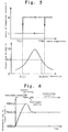
- Fig. 4 illustrates the result of the measurement of a wavelength discrimination characteristic of the waveform monitoring circuit 4 of Fig. 3.
- the graph represents a division value (1 v corresponds to the ratio 1) when an output from the optical detector 43 is divided by an output from the optical detector 44 for a wavelength of a laser signal of laser diode module 3, and indicates that a wavelength discrimination characteristic, which does not rely upon the applied power, is obtained. Since generally the oscillation wavelength of a semiconductor laser has a temperature dependency of approximately 0.1 nm/°C, the oscillation wavelength can be controlled if the wavelength discrimination curve of Fig.
- the wavelength 4 is used to control the temperature of the laser so that the division value may be fixed. For example, if the slope of the wavelength discrimination curve on the longer wavelength side is set so that the division value may be 0.5 v, that is, the reference voltage 13 of amplifier 12 is set to 0.5 v, then the wavelength is controlled to 1,555.5 nm.
- the wavelength discrimination characteristic exhibits a higher detection sensitivity with respect to the variation of the wavelength as the full width at half maximum of the optical band-pass filter 42 decreases. However, as the full width at half maximum decreases, the range within which the wavelength can be monitored decreases. If it is intended to use the wavelength discrimination characteristic for control, when control is to be started, the wavelength of the laser diode module 3 must be initially set to a value in the proximity of the slope of the wavelength discrimination curve which is used for the control.
- the arrangement being described is characterized in that the initial setting of the wavelength of a laser diode to a value in the proximity of the slope of the wavelength discrimination curve used for wavelength control is realized.
- the operation of the initial setting of the wavelength is described on the premise that, in the present arrangement, the slope of the wavelength discrimination curve of Fig. 4 on the longer wavelength side is used to control the wavelength to 1,555.5 nm as described above.
- the wavelength of the laser diode module 3 when the power supply to the present circuit is made available may possibly be on the shorter wavelength side or on the longer wavelength side of the slope of the wavelength discrimination curve of Fig. 4 depending upon the ambient temperature. If the wavelength of the laser diode module 3 is on the shorter wavelength side of the slope, it is necessary initially to set the wavelength of the laser diode module 3 to the longer wavelength side of the slope. A detailed procedure therefor will be described below.
- the oscillation frequency of the semiconductor laser has a temperature dependency of approximately 0.1 nm/°C as described above, and the temperature and the oscillation frequency of the laser diode chip have a substantially proportional relationship to each other. Therefore, by monitoring the temperature of the laser diode module 3, an approximate oscillation frequency of the laser diode module 3 can be deduced from the temperature.
- the temperature of the laser diode module 3 is detected by the temperature monitoring circuit 21 and it is determined from the temperature whether the oscillation frequency is on the shorter wavelength side or the longer wavelength slope of the discrimination curve of Fig. 4, and if the oscillation frequency is on the shorter wavelength side, then the controlling circuit 2 is selected so that temperature control by the temperature monitoring circuit 21 is performed.
- the reference voltage 23 is set to a value which corresponds to a sufficiently longer wavelength than the longer wavelength side slope of the wavelength discrimination curve of Fig. 4. Consequently, current flows through the Peltier element 33 in a heating direction, and the temperature of laser diode module 3 rises and the wavelength of the laser diode module 3 is displaced to the longer wavelength side of the slope. Thereafter, the selection is switched from the controlling circuit 2 to the controlling circuit 1 so that control according to the wavelength discrimination characteristic of the optical band-pass filter is performed to lock the oscillation frequency to 1,555.5 nm.
- the controlling circuit 1 is selected so that the oscillation frequency is locked to 1,555.5 nm by the control according to which wavelength discrimination characteristic is used.
- the switching between the controlling circuits 1, 2 is performed by the analog switch 5.
- the switching control of the analog switch 5 is performed by the comparison circuit 6.
- the comparison circuit 6 receives a voltage proportional to the result of monitoring by the temperature monitoring circuit 21 and generates an activation signal with a predetermined threshold voltage to switch the analog switch 5.
- the comparison circuit 6 is a function generator of a variable threshold voltage having a hysteresis characteristic.
- the threshold value of the comparison circuit 6 has a hysteresis width.
- the hysteresis width is set such that, as seen in Fig.
- a temperature T(H) of the laser at which switching from the controlling circuit 2 to the controlling circuit 1 should be performed is set to the longer wavelength side with respect to a temperature corresponding to a wavelength to be locked, and the laser temperature T(L) at which switching from the controlling circuit 1 to the controlling circuit 2 should be performed is set to the shorter wavelength side with respect to a center wavelength of the discrimination curve. Consequently, after the output from the comparison circuit 6 changes over to "High” once, before the output from the comparison circuit 6 changes over to "tow", the oscillation frequency of the laser diode module 3 is locked by the controlling circuit 1.
- FIG. 6 A detailed procedure for the operation in which, when a power supply is made available, the wavelength of the laser diode module 3 is on the shorter wavelength side of the slope is illustrated in Fig. 6.
- the analog switch 5 is connected to the controlling circuit 2 side and a current flows through the Peltier element 33 in a heating direction, the wavelength of laser diode module 3 is pulled up to the longer wavelength side.
- the output from the comparison circuit 6 changes over to "High", and the analog switch 5 is switched to the controlling circuit 1 side.
- the wavelength of the laser diode module 3 is pulled in to the locking wavelength side by the wavelength discrimination characteristic of the controlling circuit 1 and is locked to the wavelength of 1,555.5 nm.
Landscapes
- Physics & Mathematics (AREA)
- Condensed Matter Physics & Semiconductors (AREA)
- General Physics & Mathematics (AREA)
- Electromagnetism (AREA)
- Optics & Photonics (AREA)
- Semiconductor Lasers (AREA)
Applications Claiming Priority (2)
| Application Number | Priority Date | Filing Date | Title |
|---|---|---|---|
| JP4780798 | 1998-02-27 | ||
| JP10047807A JPH11251673A (ja) | 1998-02-27 | 1998-02-27 | レーザ信号の波長制御回路 |
Publications (3)
| Publication Number | Publication Date |
|---|---|
| EP0939470A2 true EP0939470A2 (fr) | 1999-09-01 |
| EP0939470A3 EP0939470A3 (fr) | 2001-04-25 |
| EP0939470B1 EP0939470B1 (fr) | 2008-12-24 |
Family
ID=12785647
Family Applications (1)
| Application Number | Title | Priority Date | Filing Date |
|---|---|---|---|
| EP99301478A Expired - Lifetime EP0939470B1 (fr) | 1998-02-27 | 1999-02-26 | Circuit de contrôle de la longueur d'onde d'un signal laser |
Country Status (3)
| Country | Link |
|---|---|
| US (1) | US6529534B1 (fr) |
| EP (1) | EP0939470B1 (fr) |
| JP (1) | JPH11251673A (fr) |
Cited By (8)
| Publication number | Priority date | Publication date | Assignee | Title |
|---|---|---|---|---|
| US6120190A (en) * | 1997-11-26 | 2000-09-19 | Lasertron, Inc. | Spatially variable bandpass filter monitoring and feedback control of laser wavelength especially in wavelength division multiplexing communication systems |
| WO2000052789A3 (fr) * | 1999-03-01 | 2001-01-11 | Univ California | Source laser accordable a surveillance integree de la longueur d'ondes, et mode de mise en oeuvre |
| WO2001073904A1 (fr) * | 2000-03-25 | 2001-10-04 | Marconi Communications Limited | Source de rayonnement stabilisee |
| EP1241750A1 (fr) * | 2001-03-14 | 2002-09-18 | OpNext Japan, Inc. | Circuit de stabilisation de longueur d'ondes, émetteur optique et système de transmission optique |
| US6487027B2 (en) * | 2000-04-21 | 2002-11-26 | Fujitsu Quantum Devices Limited | Optical semiconductor module having a capability of temperature regulation |
| WO2003087898A1 (fr) * | 2002-04-15 | 2003-10-23 | Mitsubishi Denki Kabushiki Kaisha | Filtre de longueur d'onde et appareil de suivi de longueur d'onde |
| GB2402544A (en) * | 2003-06-03 | 2004-12-08 | Agilent Technologies Inc | Electromagnetic Radiation Emission Apparatus |
| EP3022514A4 (fr) * | 2013-07-15 | 2017-01-18 | Optiflow, Inc. | Viseur |
Families Citing this family (21)
| Publication number | Priority date | Publication date | Assignee | Title |
|---|---|---|---|---|
| WO2002075935A2 (fr) * | 2001-03-15 | 2002-09-26 | Iolon, Inc. | Appareil de syntonisation et de verrouillage des frequences, et procede de mise en oeuvre de l'appareil |
| JP2002319736A (ja) * | 2001-04-23 | 2002-10-31 | Furukawa Electric Co Ltd:The | レーザ光の波長調整装置 |
| EP1265325A1 (fr) * | 2001-06-08 | 2002-12-11 | Alcatel | Dispositif optique comportant un étalon termiquement stable |
| US7941056B2 (en) | 2001-08-30 | 2011-05-10 | Micron Technology, Inc. | Optical interconnect in high-speed memory systems |
| JP2003163407A (ja) * | 2001-11-28 | 2003-06-06 | Fujitsu Ltd | 光半導体装置 |
| US6785308B2 (en) * | 2002-03-28 | 2004-08-31 | Nortel Networks Limited | Spectral conditioning system and method |
| JP2003318481A (ja) | 2002-04-25 | 2003-11-07 | Sumitomo Electric Ind Ltd | レーザ制御回路およびレーザモジュール |
| JP3766347B2 (ja) * | 2002-05-16 | 2006-04-12 | 東芝電子エンジニアリング株式会社 | 光送信用デバイス |
| US6904067B2 (en) * | 2002-10-03 | 2005-06-07 | Intel Corporation | Back facet wavelength locker tuning and assembly method |
| JP2004221267A (ja) * | 2003-01-14 | 2004-08-05 | Nippon Telegr & Teleph Corp <Ntt> | 高速波長可変分布帰還型半導体レーザアレイ及び分布帰還型半導体レーザ |
| JP2006173213A (ja) * | 2004-12-13 | 2006-06-29 | Advantest Corp | 温度安定化装置及び発振装置 |
| US7693420B2 (en) * | 2005-08-09 | 2010-04-06 | The Boeing Company | Thermal drift compensation system and method for optical networks |
| US7975493B2 (en) * | 2006-02-10 | 2011-07-12 | Finisar Corporation | Thermoelectric cooler with inrush current control |
| JP2006324636A (ja) * | 2006-03-03 | 2006-11-30 | Yamatake Corp | レーザ発振波長検出方法、制御方法および装置 |
| GB2454693A (en) * | 2007-11-15 | 2009-05-20 | Bookham Technology Plc | Optical amplifiers |
| JP2010232336A (ja) * | 2009-03-26 | 2010-10-14 | Fujitsu Optical Components Ltd | 光源制御装置および光源装置 |
| JP2010258350A (ja) * | 2009-04-28 | 2010-11-11 | Sanyo Electric Co Ltd | 発光装置、情報取得装置および物体検出装置 |
| JP6319718B2 (ja) * | 2013-11-29 | 2018-05-09 | 住友電工デバイス・イノベーション株式会社 | 波長可変レーザの制御方法 |
| CN104300360B (zh) * | 2014-10-16 | 2018-04-20 | 浙江大学 | 一种改善超辐射发光二极管光源波长稳定性的装置和方法 |
| DE102018209995A1 (de) | 2018-06-20 | 2019-12-24 | Robert Bosch Gmbh | Stabilisiertes LiDAR-System und Verfahren zur Stabilisierung |
| DE102018128630B4 (de) | 2018-11-15 | 2025-04-03 | Sick Ag | Sensoren und Verfahren zur Erfassung von Objekten |
Family Cites Families (17)
| Publication number | Priority date | Publication date | Assignee | Title |
|---|---|---|---|---|
| JPH0728077B2 (ja) | 1986-04-16 | 1995-03-29 | 株式会社トプコン | 半導体レ−ザ−の発振周波数・発振出力安定化装置 |
| JPS63143888A (ja) | 1986-12-08 | 1988-06-16 | Yokogawa Electric Corp | レ−ザ発生装置の制御方法 |
| GB2224389B (en) * | 1988-10-20 | 1993-04-21 | Mitsubishi Electric Corp | Laser device with wavelength stabilization control and method of operating the same |
| JP3490476B2 (ja) | 1993-04-20 | 2004-01-26 | オリンパス株式会社 | 波長安定化装置 |
| US5438579A (en) * | 1992-12-18 | 1995-08-01 | Olympus Optical Co., Ltd. | Wavelength stabilizing apparatus |
| JPH07249817A (ja) | 1994-03-09 | 1995-09-26 | Toshiba Corp | 波長安定化光源 |
| JPH0818145A (ja) | 1994-04-28 | 1996-01-19 | Olympus Optical Co Ltd | 波長安定化装置 |
| JPH07302948A (ja) | 1994-05-02 | 1995-11-14 | Olympus Optical Co Ltd | 波長安定化装置 |
| JP3006822B2 (ja) | 1994-07-22 | 2000-02-07 | 日本電気株式会社 | レーザ波長制御装置 |
| JP2626593B2 (ja) | 1994-11-14 | 1997-07-02 | 日本電気株式会社 | 電子冷却付レーザーモジュールの駆動回路 |
| JPH08237203A (ja) * | 1995-02-23 | 1996-09-13 | Fujitsu Ltd | 光フィルタアレイ、光送信機及び光送信システム |
| JP3681447B2 (ja) * | 1995-10-25 | 2005-08-10 | 富士通株式会社 | 光波長安定化システム |
| JPH09219554A (ja) | 1996-02-08 | 1997-08-19 | Nippon Telegr & Teleph Corp <Ntt> | 半導体レーザダイオードの光出力制御装置 |
| JP2871623B2 (ja) | 1996-07-11 | 1999-03-17 | 日本電気株式会社 | 半導体レーザ装置 |
| JPH10164018A (ja) * | 1996-11-26 | 1998-06-19 | Fujitsu Ltd | 光送信機並びに該光送信機を有する端局装置及び光通信システム |
| JP4124845B2 (ja) * | 1997-10-24 | 2008-07-23 | 日本オプネクスト株式会社 | 光波長安定制御装置 |
| JP3139435B2 (ja) * | 1998-01-05 | 2001-02-26 | 日本電気株式会社 | レーザダイオード光波長制御装置 |
-
1998
- 1998-02-27 JP JP10047807A patent/JPH11251673A/ja active Pending
-
1999
- 1999-02-11 US US09/249,240 patent/US6529534B1/en not_active Expired - Fee Related
- 1999-02-26 EP EP99301478A patent/EP0939470B1/fr not_active Expired - Lifetime
Cited By (11)
| Publication number | Priority date | Publication date | Assignee | Title |
|---|---|---|---|---|
| US6120190A (en) * | 1997-11-26 | 2000-09-19 | Lasertron, Inc. | Spatially variable bandpass filter monitoring and feedback control of laser wavelength especially in wavelength division multiplexing communication systems |
| US6371662B1 (en) | 1997-11-26 | 2002-04-16 | Corning Lasertron, Inc. | Spatially variable filter laser wavelength monitoring/control |
| WO2000052789A3 (fr) * | 1999-03-01 | 2001-01-11 | Univ California | Source laser accordable a surveillance integree de la longueur d'ondes, et mode de mise en oeuvre |
| WO2001073904A1 (fr) * | 2000-03-25 | 2001-10-04 | Marconi Communications Limited | Source de rayonnement stabilisee |
| US6933485B2 (en) | 2000-03-25 | 2005-08-23 | Marconi Lik Intellectual Property Ltd. | Stabilizing power and wavelength of output radiation from a stabilized radiation source in optical communications systems |
| US6487027B2 (en) * | 2000-04-21 | 2002-11-26 | Fujitsu Quantum Devices Limited | Optical semiconductor module having a capability of temperature regulation |
| EP1241750A1 (fr) * | 2001-03-14 | 2002-09-18 | OpNext Japan, Inc. | Circuit de stabilisation de longueur d'ondes, émetteur optique et système de transmission optique |
| US6693932B2 (en) | 2001-03-14 | 2004-02-17 | Opnext Japan, Inc. | Optical wavelength stabilization circuit, optical transmitter and optical transmission system |
| WO2003087898A1 (fr) * | 2002-04-15 | 2003-10-23 | Mitsubishi Denki Kabushiki Kaisha | Filtre de longueur d'onde et appareil de suivi de longueur d'onde |
| GB2402544A (en) * | 2003-06-03 | 2004-12-08 | Agilent Technologies Inc | Electromagnetic Radiation Emission Apparatus |
| EP3022514A4 (fr) * | 2013-07-15 | 2017-01-18 | Optiflow, Inc. | Viseur |
Also Published As
| Publication number | Publication date |
|---|---|
| JPH11251673A (ja) | 1999-09-17 |
| EP0939470B1 (fr) | 2008-12-24 |
| EP0939470A3 (fr) | 2001-04-25 |
| US6529534B1 (en) | 2003-03-04 |
Similar Documents
| Publication | Publication Date | Title |
|---|---|---|
| EP0939470B1 (fr) | Circuit de contrôle de la longueur d'onde d'un signal laser | |
| US6101200A (en) | Laser module allowing simultaneous wavelength and power control | |
| EP1215832B1 (fr) | Emetteur optique à longueur d'onde variable avec contrôle d'émission, et système de communication optique correspondant | |
| EP0732786B1 (fr) | Méthode et dispositif pour l'amplification optique | |
| US4309671A (en) | Control apparatus | |
| US6008935A (en) | Optical amplifier and optical amplifier gain control method and apparatus | |
| US20090003843A1 (en) | Optical transmitter and method for control the same | |
| US20030030876A1 (en) | Optical transmitter, optical receiver and light wavelength multiplexing system | |
| US6518563B1 (en) | Detecting aging of optical components | |
| EP1269589B1 (fr) | Source de rayonnement stabilisee | |
| US6965622B1 (en) | Wavelength locking scheme and algorithm for ultra-high density WDM system | |
| JP4222469B2 (ja) | 波長モニタ及び半導体レーザモジュール | |
| JP4336091B2 (ja) | 光モジュール、光送信器及びwdm光送信装置 | |
| JP2546151B2 (ja) | レーザダイオード発光波長制御装置 | |
| JP3180746B2 (ja) | 光増幅装置並びに光増幅器利得制御方法及び装置 | |
| JP2002537662A (ja) | 同調可能なレーザーの波長をロックし、モードをモニタする方法 | |
| US20090047014A1 (en) | Optical transmitting module and a method to sense a fluctuation of light emitted from the same | |
| US6449077B1 (en) | Method and apparatus for electrically switching a wavelength control system | |
| EP1608088A1 (fr) | Méthode et appareil pour transmettre un signal optique | |
| JP2694803B2 (ja) | 光半導体レーザ装置の波長安定化方式 | |
| KR100236832B1 (ko) | 파장분할다중 방식에서 파장 안정화부를 가지는 송신장치 및 구현방법 | |
| JP3006822B2 (ja) | レーザ波長制御装置 | |
| JPH0834328B2 (ja) | Ld発光波長制御装置 | |
| JP2003283043A (ja) | 発振モードモニタ装置および半導体レーザ装置 | |
| US6441940B1 (en) | Wavelength stabilization of light emitting components |
Legal Events
| Date | Code | Title | Description |
|---|---|---|---|
| PUAI | Public reference made under article 153(3) epc to a published international application that has entered the european phase |
Free format text: ORIGINAL CODE: 0009012 |
|
| AK | Designated contracting states |
Kind code of ref document: A2 Designated state(s): FR GB |
|
| AX | Request for extension of the european patent |
Free format text: AL;LT;LV;MK;RO;SI |
|
| PUAL | Search report despatched |
Free format text: ORIGINAL CODE: 0009013 |
|
| AK | Designated contracting states |
Kind code of ref document: A3 Designated state(s): AT BE CH CY DE DK ES FI FR GB GR IE IT LI LU MC NL PT SE |
|
| AX | Request for extension of the european patent |
Free format text: AL;LT;LV;MK;RO;SI |
|
| 17P | Request for examination filed |
Effective date: 20010321 |
|
| 17Q | First examination report despatched |
Effective date: 20011102 |
|
| AKX | Designation fees paid |
Free format text: FR GB |
|
| REG | Reference to a national code |
Ref country code: DE Ref legal event code: 8566 |
|
| GRAP | Despatch of communication of intention to grant a patent |
Free format text: ORIGINAL CODE: EPIDOSNIGR1 |
|
| RIC1 | Information provided on ipc code assigned before grant |
Ipc: H01S 5/0683 20060101AFI20080711BHEP |
|
| GRAS | Grant fee paid |
Free format text: ORIGINAL CODE: EPIDOSNIGR3 |
|
| GRAA | (expected) grant |
Free format text: ORIGINAL CODE: 0009210 |
|
| AK | Designated contracting states |
Kind code of ref document: B1 Designated state(s): FR GB |
|
| REG | Reference to a national code |
Ref country code: GB Ref legal event code: FG4D |
|
| PLBE | No opposition filed within time limit |
Free format text: ORIGINAL CODE: 0009261 |
|
| STAA | Information on the status of an ep patent application or granted ep patent |
Free format text: STATUS: NO OPPOSITION FILED WITHIN TIME LIMIT |
|
| 26N | No opposition filed |
Effective date: 20090925 |
|
| PGFP | Annual fee paid to national office [announced via postgrant information from national office to epo] |
Ref country code: FR Payment date: 20100223 Year of fee payment: 12 |
|
| PGFP | Annual fee paid to national office [announced via postgrant information from national office to epo] |
Ref country code: GB Payment date: 20100202 Year of fee payment: 12 |
|
| GBPC | Gb: european patent ceased through non-payment of renewal fee |
Effective date: 20110226 |
|
| REG | Reference to a national code |
Ref country code: FR Ref legal event code: ST Effective date: 20111102 |
|
| PG25 | Lapsed in a contracting state [announced via postgrant information from national office to epo] |
Ref country code: FR Free format text: LAPSE BECAUSE OF NON-PAYMENT OF DUE FEES Effective date: 20110228 |
|
| PG25 | Lapsed in a contracting state [announced via postgrant information from national office to epo] |
Ref country code: GB Free format text: LAPSE BECAUSE OF NON-PAYMENT OF DUE FEES Effective date: 20110226 |