EP0940797B1 - Anzeigevorrichtung mit aktiver matrix - Google Patents
Anzeigevorrichtung mit aktiver matrix Download PDFInfo
- Publication number
- EP0940797B1 EP0940797B1 EP98938919A EP98938919A EP0940797B1 EP 0940797 B1 EP0940797 B1 EP 0940797B1 EP 98938919 A EP98938919 A EP 98938919A EP 98938919 A EP98938919 A EP 98938919A EP 0940797 B1 EP0940797 B1 EP 0940797B1
- Authority
- EP
- European Patent Office
- Prior art keywords
- film
- insulating layer
- bank
- active matrix
- display device
- Prior art date
- Legal status (The legal status is an assumption and is not a legal conclusion. Google has not performed a legal analysis and makes no representation as to the accuracy of the status listed.)
- Expired - Lifetime
Links
- 239000011159 matrix material Substances 0.000 title claims description 104
- 239000010408 film Substances 0.000 claims description 304
- 239000010409 thin film Substances 0.000 claims description 47
- 238000000034 method Methods 0.000 claims description 35
- 229910010272 inorganic material Inorganic materials 0.000 claims description 32
- 239000011147 inorganic material Substances 0.000 claims description 32
- 230000008569 process Effects 0.000 claims description 31
- 239000000758 substrate Substances 0.000 claims description 27
- 239000011368 organic material Substances 0.000 claims description 21
- 230000002093 peripheral effect Effects 0.000 claims description 9
- 230000000740 bleeding effect Effects 0.000 claims description 7
- 239000010410 layer Substances 0.000 description 345
- 230000015572 biosynthetic process Effects 0.000 description 24
- 230000003071 parasitic effect Effects 0.000 description 22
- 239000003990 capacitor Substances 0.000 description 19
- 230000003247 decreasing effect Effects 0.000 description 19
- 238000010586 diagram Methods 0.000 description 14
- VYPSYNLAJGMNEJ-UHFFFAOYSA-N Silicium dioxide Chemical compound O=[Si]=O VYPSYNLAJGMNEJ-UHFFFAOYSA-N 0.000 description 13
- 229920001721 polyimide Polymers 0.000 description 13
- 229910052814 silicon oxide Inorganic materials 0.000 description 13
- 239000000243 solution Substances 0.000 description 13
- 229910052581 Si3N4 Inorganic materials 0.000 description 12
- 239000011229 interlayer Substances 0.000 description 12
- HQVNEWCFYHHQES-UHFFFAOYSA-N silicon nitride Chemical compound N12[Si]34N5[Si]62N3[Si]51N64 HQVNEWCFYHHQES-UHFFFAOYSA-N 0.000 description 12
- 239000002243 precursor Substances 0.000 description 10
- 230000000694 effects Effects 0.000 description 9
- 238000005530 etching Methods 0.000 description 8
- 230000004048 modification Effects 0.000 description 8
- 238000012986 modification Methods 0.000 description 8
- 238000000059 patterning Methods 0.000 description 7
- 238000000623 plasma-assisted chemical vapour deposition Methods 0.000 description 7
- 230000006866 deterioration Effects 0.000 description 5
- BOTDANWDWHJENH-UHFFFAOYSA-N Tetraethyl orthosilicate Chemical compound CCO[Si](OCC)(OCC)OCC BOTDANWDWHJENH-UHFFFAOYSA-N 0.000 description 4
- 238000000151 deposition Methods 0.000 description 4
- 230000008021 deposition Effects 0.000 description 4
- 238000002347 injection Methods 0.000 description 4
- 239000007924 injection Substances 0.000 description 4
- 239000004973 liquid crystal related substance Substances 0.000 description 4
- 239000005871 repellent Substances 0.000 description 4
- 230000007547 defect Effects 0.000 description 3
- 238000007599 discharging Methods 0.000 description 3
- 239000011344 liquid material Substances 0.000 description 3
- 238000004020 luminiscence type Methods 0.000 description 3
- 239000002904 solvent Substances 0.000 description 3
- 229910052782 aluminium Inorganic materials 0.000 description 2
- XAGFODPZIPBFFR-UHFFFAOYSA-N aluminium Chemical compound [Al] XAGFODPZIPBFFR-UHFFFAOYSA-N 0.000 description 2
- 229910021417 amorphous silicon Inorganic materials 0.000 description 2
- QVGXLLKOCUKJST-UHFFFAOYSA-N atomic oxygen Chemical compound [O] QVGXLLKOCUKJST-UHFFFAOYSA-N 0.000 description 2
- 230000004888 barrier function Effects 0.000 description 2
- 238000000576 coating method Methods 0.000 description 2
- 230000000052 comparative effect Effects 0.000 description 2
- 230000000295 complement effect Effects 0.000 description 2
- 239000007789 gas Substances 0.000 description 2
- 238000010438 heat treatment Methods 0.000 description 2
- 238000004519 manufacturing process Methods 0.000 description 2
- 239000000463 material Substances 0.000 description 2
- 229910052751 metal Inorganic materials 0.000 description 2
- 239000002184 metal Substances 0.000 description 2
- 229910052760 oxygen Inorganic materials 0.000 description 2
- 239000001301 oxygen Substances 0.000 description 2
- 229920000553 poly(phenylenevinylene) Polymers 0.000 description 2
- -1 polyphenylene vinylene Polymers 0.000 description 2
- 230000001681 protective effect Effects 0.000 description 2
- 239000002356 single layer Substances 0.000 description 2
- 238000004544 sputter deposition Methods 0.000 description 2
- OYPRJOBELJOOCE-UHFFFAOYSA-N Calcium Chemical compound [Ca] OYPRJOBELJOOCE-UHFFFAOYSA-N 0.000 description 1
- WHXSMMKQMYFTQS-UHFFFAOYSA-N Lithium Chemical compound [Li] WHXSMMKQMYFTQS-UHFFFAOYSA-N 0.000 description 1
- ZOKXTWBITQBERF-UHFFFAOYSA-N Molybdenum Chemical compound [Mo] ZOKXTWBITQBERF-UHFFFAOYSA-N 0.000 description 1
- XUIMIQQOPSSXEZ-UHFFFAOYSA-N Silicon Chemical compound [Si] XUIMIQQOPSSXEZ-UHFFFAOYSA-N 0.000 description 1
- RTAQQCXQSZGOHL-UHFFFAOYSA-N Titanium Chemical compound [Ti] RTAQQCXQSZGOHL-UHFFFAOYSA-N 0.000 description 1
- 238000009825 accumulation Methods 0.000 description 1
- 229910052791 calcium Inorganic materials 0.000 description 1
- 239000011575 calcium Substances 0.000 description 1
- 238000002425 crystallisation Methods 0.000 description 1
- 230000008025 crystallization Effects 0.000 description 1
- 238000005265 energy consumption Methods 0.000 description 1
- 239000012535 impurity Substances 0.000 description 1
- AMGQUBHHOARCQH-UHFFFAOYSA-N indium;oxotin Chemical compound [In].[Sn]=O AMGQUBHHOARCQH-UHFFFAOYSA-N 0.000 description 1
- 238000009434 installation Methods 0.000 description 1
- 238000009413 insulation Methods 0.000 description 1
- 230000001788 irregular Effects 0.000 description 1
- 238000005224 laser annealing Methods 0.000 description 1
- 229910052744 lithium Inorganic materials 0.000 description 1
- 229910052750 molybdenum Inorganic materials 0.000 description 1
- 239000011733 molybdenum Substances 0.000 description 1
- 229910052698 phosphorus Inorganic materials 0.000 description 1
- 239000011574 phosphorus Substances 0.000 description 1
- 229910021420 polycrystalline silicon Inorganic materials 0.000 description 1
- 229920005591 polysilicon Polymers 0.000 description 1
- 230000002035 prolonged effect Effects 0.000 description 1
- 230000009467 reduction Effects 0.000 description 1
- 229910052710 silicon Inorganic materials 0.000 description 1
- 239000010703 silicon Substances 0.000 description 1
- 239000007790 solid phase Substances 0.000 description 1
- 238000003860 storage Methods 0.000 description 1
- 229910052715 tantalum Inorganic materials 0.000 description 1
- GUVRBAGPIYLISA-UHFFFAOYSA-N tantalum atom Chemical compound [Ta] GUVRBAGPIYLISA-UHFFFAOYSA-N 0.000 description 1
- 229910052719 titanium Inorganic materials 0.000 description 1
- 239000010936 titanium Substances 0.000 description 1
- WFKWXMTUELFFGS-UHFFFAOYSA-N tungsten Chemical compound [W] WFKWXMTUELFFGS-UHFFFAOYSA-N 0.000 description 1
- 229910052721 tungsten Inorganic materials 0.000 description 1
- 239000010937 tungsten Substances 0.000 description 1
Images








Classifications
-
- H—ELECTRICITY
- H10—SEMICONDUCTOR DEVICES; ELECTRIC SOLID-STATE DEVICES NOT OTHERWISE PROVIDED FOR
- H10K—ORGANIC ELECTRIC SOLID-STATE DEVICES
- H10K59/00—Integrated devices, or assemblies of multiple devices, comprising at least one organic light-emitting element covered by group H10K50/00
- H10K59/10—OLED displays
- H10K59/12—Active-matrix OLED [AMOLED] displays
- H10K59/122—Pixel-defining structures or layers, e.g. banks
-
- G—PHYSICS
- G09—EDUCATION; CRYPTOGRAPHY; DISPLAY; ADVERTISING; SEALS
- G09F—DISPLAYING; ADVERTISING; SIGNS; LABELS OR NAME-PLATES; SEALS
- G09F9/00—Indicating arrangements for variable information in which the information is built-up on a support by selection or combination of individual elements
- G09F9/30—Indicating arrangements for variable information in which the information is built-up on a support by selection or combination of individual elements in which the desired character or characters are formed by combining individual elements
-
- H—ELECTRICITY
- H10—SEMICONDUCTOR DEVICES; ELECTRIC SOLID-STATE DEVICES NOT OTHERWISE PROVIDED FOR
- H10K—ORGANIC ELECTRIC SOLID-STATE DEVICES
- H10K50/00—Organic light-emitting devices
- H10K50/80—Constructional details
- H10K50/805—Electrodes
-
- H—ELECTRICITY
- H10—SEMICONDUCTOR DEVICES; ELECTRIC SOLID-STATE DEVICES NOT OTHERWISE PROVIDED FOR
- H10K—ORGANIC ELECTRIC SOLID-STATE DEVICES
- H10K59/00—Integrated devices, or assemblies of multiple devices, comprising at least one organic light-emitting element covered by group H10K50/00
- H10K59/10—OLED displays
- H10K59/12—Active-matrix OLED [AMOLED] displays
- H10K59/131—Interconnections, e.g. wiring lines or terminals
-
- H—ELECTRICITY
- H10—SEMICONDUCTOR DEVICES; ELECTRIC SOLID-STATE DEVICES NOT OTHERWISE PROVIDED FOR
- H10K—ORGANIC ELECTRIC SOLID-STATE DEVICES
- H10K59/00—Integrated devices, or assemblies of multiple devices, comprising at least one organic light-emitting element covered by group H10K50/00
- H10K59/80—Constructional details
- H10K59/805—Electrodes
-
- H—ELECTRICITY
- H10—SEMICONDUCTOR DEVICES; ELECTRIC SOLID-STATE DEVICES NOT OTHERWISE PROVIDED FOR
- H10K—ORGANIC ELECTRIC SOLID-STATE DEVICES
- H10K50/00—Organic light-emitting devices
- H10K50/80—Constructional details
- H10K50/86—Arrangements for improving contrast, e.g. preventing reflection of ambient light
- H10K50/865—Arrangements for improving contrast, e.g. preventing reflection of ambient light comprising light absorbing layers, e.g. light-blocking layers
-
- H—ELECTRICITY
- H10—SEMICONDUCTOR DEVICES; ELECTRIC SOLID-STATE DEVICES NOT OTHERWISE PROVIDED FOR
- H10K—ORGANIC ELECTRIC SOLID-STATE DEVICES
- H10K59/00—Integrated devices, or assemblies of multiple devices, comprising at least one organic light-emitting element covered by group H10K50/00
- H10K59/30—Devices specially adapted for multicolour light emission
- H10K59/35—Devices specially adapted for multicolour light emission comprising red-green-blue [RGB] subpixels
-
- H—ELECTRICITY
- H10—SEMICONDUCTOR DEVICES; ELECTRIC SOLID-STATE DEVICES NOT OTHERWISE PROVIDED FOR
- H10K—ORGANIC ELECTRIC SOLID-STATE DEVICES
- H10K59/00—Integrated devices, or assemblies of multiple devices, comprising at least one organic light-emitting element covered by group H10K50/00
- H10K59/80—Constructional details
- H10K59/8791—Arrangements for improving contrast, e.g. preventing reflection of ambient light
- H10K59/8792—Arrangements for improving contrast, e.g. preventing reflection of ambient light comprising light absorbing layers, e.g. black layers
-
- H—ELECTRICITY
- H10—SEMICONDUCTOR DEVICES; ELECTRIC SOLID-STATE DEVICES NOT OTHERWISE PROVIDED FOR
- H10K—ORGANIC ELECTRIC SOLID-STATE DEVICES
- H10K71/00—Manufacture or treatment specially adapted for the organic devices covered by this subclass
- H10K71/10—Deposition of organic active material
- H10K71/12—Deposition of organic active material using liquid deposition, e.g. spin coating
- H10K71/13—Deposition of organic active material using liquid deposition, e.g. spin coating using printing techniques, e.g. ink-jet printing or screen printing
- H10K71/135—Deposition of organic active material using liquid deposition, e.g. spin coating using printing techniques, e.g. ink-jet printing or screen printing using ink-jet printing
Definitions
- the present invention relates to active matrix display devices which control thin film luminescent devices, such as electroluminescent (EL) devices emitting light by a driving current flowing in an organic semiconductive film, and light-emitting diode (LED) devices using thin film transistors (hereinafter referred to as TFTs).
- thin film luminescent devices such as electroluminescent (EL) devices emitting light by a driving current flowing in an organic semiconductive film, and light-emitting diode (LED) devices using thin film transistors (hereinafter referred to as TFTs).
- Active matrix display devices using current-control-type luminescent devices such as EL devices or LED devices have been proposed. Since luminescent devices used in such types of display devices have self-luminescent functions; these have advantages, such as no installation of a backlight being necessary, whereas backlights are essential for liquid crystal display devices, and a wider viewing angle.
- TFT-EL thin-film-transistor-electroluminescent
- Fig. 22 is a block diagram of an active matrix display device using charge-injection-type organic EL devices.
- a plurality of scanning lines gate a plurality of data lines sig extending in the direction perpendicular to the direction of the scanning lines gate , a plurality of common feed lines com along the data lines sig , and a plurality of pixels 7 in a matrix formed by the data lines sig and the scanning lines gate are formed on a transparent substrate 10.
- a data line driving circuit 3 and a scanning line driving circuit 4 are provided for the data lines sig and the scanning lines gate , respectively.
- Each pixel 7 is provided with a conduction control circuit 50 for supplying scanning signals from a scanning line gate , and a thin film luminescent device 40 emitting light based on image signals supplied from a data line sig through the conduction control circuit 50.
- the conduction control circuit 50 has a first TFT 20 for supplying scanning signals from the scanning line gate to a gate electrode; a holding capacitor cap for holding image signals supplied from the data line sig through the first TFT 20; and a second TFT 30 for supplying the image signals held in the holding capacitor cap to the gate electrode.
- the second TFT 30 and the thin film luminescent device 40 are connected in series between an opposite electrode op (described below) and a common feed line com .
- the thin film luminescent device 40 emits light by a driving current from the common feed line com when the second TFT 30 is an ON mode, and this emitting mode is maintained by a holding capacitor cap for a predetermined time.
- the first TFT 20 and the second TFT 30 are formed of islands of a semiconductive film in each pixel 7.
- the first TFT 20 is provided with a gate electrode 21 as a part of a scanning line gate.
- one source-drain region is electrically connected to a data line sig through a contact hole in a first insulating interlayer 51, and the other region is connected to a drain electrode 22.
- the drain electrode 22 extends towards the region of the second TFT 30, and this extension is electrically connected to a gate electrode 31 of the second TFT 30 through a contact hole in the first insulating interlayer 51.
- One source-drain region of the second TFT 30 is electrically connected to a relay electrode 35 through a contact hole of the first insulating interlayer 51, and the relay electrode 35 is electrically connected to a pixel electrode 41 of the thin film luminescent device 40 through a contact hole in a second insulating interlayer 52.
- Each pixel electrode 41 is independently formed in each pixel 7, as shown in Figs. 23, 24(B), and 24(C).
- An organic semiconductive film 43 and an opposite electrode op are formed above the pixel electrode 41 in that order.
- the organic semiconductive film 43 is formed in each pixel 7, a stripe film may be formed over a plurality of pixels 7.
- the opposite electrode op is formed not only in a display section 11 including pixels 7, but also over the entire surface of the transparent substrate 10.
- the other source-drain region of the second TFT 30 is electrically connected to the common feed line com through a contact hole in the first insulating interlayer 51.
- An extension 39 of the common feed line com faces an extension 36 of the gate electrode 31 in the second TFT 30 separated by the first insulating interlayer 51 as a dielectric film to form a holding capacitor cap .
- the second insulating interlayer 52 is disposed between the opposite electrode op facing the pixel electrode 41 and the data line sig on the same transparent substrate 10, unlike liquid crystal active matrix display devices; hence, a large capacitance is formed in the data line sig and the data line driving circuit 3 is heavily loaded.
- the present inventors propose a reduction in parasitic capacitance in the data line sig by providing a thick insulating film (a bank layer bank; the region shaded with lines slanting downward to the left at a wide pitch) between the opposite electrode op and the data line sig. Furthermore, the present inventors propose that the region for forming the organic semiconductive film 43 be surrounded with the insulating film (bank layer bank ) to contain any solution discharged from an ink-jet head and to prevent bleeding of the solution towards the sides during formation of the organic semiconductive film 43.
- the entire bank layer bank is formed of a thick inorganic material in adoption of such a configuration, a problem of a prolonged film forming time arises.
- the thick inorganic film is patterned, the pixel electrode 41 may be damaged due to overetching.
- the bank layer bank is formed of an organic material, such as a resist, the organic semiconductive film 43 may deteriorate at the boundary between the organic semiconductive film 43 and the bank layer bank by the effects of the solvent components contained in the organic material in the bank layer bank .
- the opposite electrode op formed above the bank layer bank readily breaks on the step difference bb. Such breakage of the opposite electrode op due to the step difference bb causes insulation of the opposite electrode op from the neighboring opposite electrodes op to form point or linear defects in the display.
- the opposite electrode op breaks along the outer periphery of the bank layer bank which covers the surfaces of the data line driving circuit 3 and the scanning line driving circuit 4, the opposite electrode op in the display section 11 is completely insulated from a terminal 12 and thus no image is displayed.
- an active matrix display device comprising a display region including a plurality of scanning lines on a substrate, a plurality of data lines extending in the direction perpendicular to the direction of the scanning lines, and a plurality of pixels arranged in a matrix delimited by the data lines and the scanning lines; each of the pixels being provided with a thin film luminescent device having a conduction control circuit containing a thin film transistor for supplying a scanning signal to a gate electrode through one of the scanning lines, a pixel electrode, an organic semiconductive film deposited above the pixel electrode, and an opposite electrode deposited above the organic semiconductive film; the thin film luminescent device emitting light based on an image signal supplied from the data line through the conduction control circuit; wherein the region for forming the organic semiconductive film is divided by an insulating film which is thicker than the organic semiconductive film; and the insulating film comprises a lower insulating layer which is formed of an inorganic material and is thicker
- the data line will form large parasitic capacitance if the opposite electrode is formed on the entire surface of the display section to face the data line; however, a thick insulating film is provided between the data line and the opposite electrode in the present invention to prevent formation of the parasitic capacitance in the data line.
- a load on the data line driving circuit is reduced, and low energy consumption and high-speed display operation are achieved.
- the thick insulating film is formed of only an inorganic material, a long film deposition time is required, resulting in low productivity.
- the lower insulating layer in contact with the organic semiconductive film of the thin film luminescent device is formed of an inorganic material, and an upper insulating layer composed of an organic material such as a resist is formed thereon. Since the upper insulating layer composed of an organic material facilitates formation of a thick film and so results in improved productivity.
- the upper insulating layer does not come into contact with the organic semiconductive film, but the lower insulating layer composed of an inorganic material does come into contact with the organic semiconductive film; hence, the organic semiconductive film is protected from deterioration affected by the upper insulating layer. Accordingly, the thin film luminescent device does not have any decreased luminescent efficiency or reliability.
- the upper insulating layer be deposited in an inner region of the lower insulating layer so as to have a width narrower than that of the upper insulating layer.
- Such a two-step configuration prevents contact of the upper insulating layer composed of an organic material with the organic semiconductive film; hence deterioration of the organic semiconductive film can be more securely prevented.
- both the lower insulating layer and the upper insulating layer may be formed of inorganic materials.
- Another aspect of the present invention is an active matrix display device comprising a display region including a plurality of scanning lines on a substrate, a plurality of data lines extending in the direction perpendicular to the direction of the scanning lines, and a plurality of pixels arranged in a matrix delimited by the data lines and the scanning lines; each of the pixels being provided with a thin film luminescent device having a conduction control circuit containing a thin film transistor for supplying a scanning signal to a gate electrode through one of the scanning lines, a pixel electrode, an organic semiconductive film deposited above the pixel electrode, and an opposite electrode deposited above the organic semiconductive film; the thin film luminescent device emitting light based on an image signal supplied from the data line through the conduction control circuit; wherein the region for forming the organic semiconductive film is divided by an insulating film which is thicker than the organic semiconductive film; and the insulating
- the upper insulating layer is patterned. Since the lower insulating layer functions as an etching stopper, the pixel electrodes will not be damaged by slight overetching. After the patterning, the lower insulating layer is patterned. Since only one layer of the lower insulating layer is etched, the etching is readily controlled so that overetching, which would damage the pixel electrodes, does not occur.
- the conduction control circuit be provided with a first TFT for supplying the scanning signal to the gate electrode and a second TFT of which the gate electrode is connected to the data line through the first TFT, and that the second TFT and the thin film luminescent device be connected in series between a common feed line formed in addition to the data line and the scanning line for supplying a drive current and the opposite electrode.
- the conduction control circuit can be composed of a TFT and a holding capacitor
- the conduction control circuit of each pixel is preferably composed of two TFTs and two holding capacitors for improving display quality.
- the insulating film be used as a bank layer which prevents bleeding of a discharged solution when the organic semiconductive film is formed by an ink-jet process in a region delimited by the insulating film.
- the insulating film preferably has a thickness of 1 ⁇ m or more.
- a region overlapping the area for forming the conduction control circuit in the region for forming the pixel electrode be covered with the insulating film. That is, it is preferable that within the region for forming the pixel electrode, the thick insulating film be opened only at the flat section not having the conduction control circuit and the organic semiconductive film be formed only at the interior thereof.
- the thick insulating film be opened only at the flat section not having the conduction control circuit and the organic semiconductive film be formed only at the interior thereof.
- Such a configuration can prevent display irregularities due to an irregular thickness of the organic semiconductive film.
- a thinner section of the organic semiconductive film causes a concentration of the driving current of the thin film luminescent device and decreased reliability; however, this configuration can prevent such a problem.
- the organic semiconductive film emits light due to a driving current between a pixel electrode and the opposite electrode in the region overlapping the conduction control circuit, the light is shaded by the conduction control circuit and does not contribute to display.
- the driving current not contributing to display by the shading effect of the conduction control circuit is an unavailable current.
- the thick insulating film is formed at the section, in which such an unavailable current is expected, to prevent formation of the unavailable current.
- a current in the common feed line can be reduced.
- a luminescent area can be increased, improving display characteristics, such as luminance and contrast.
- the corners delimited by the insulating film may be rounded so that the organic semiconductive film has a rounded planar shape.
- the organic semiconductive film having such a shape avoids the concentration of the driving current at the corners, hence defects, such as insufficient voltage resistance, can be prevented at the corners.
- the lower insulating layer of the insulating film is formed so as to cover the area for forming the conduction control circuit in the region for forming the pixel electrode, the data line, the common feed line, and the scanning line, whereas the upper insulating layer is formed so as to form a striped pattern along the data line, and the organic semiconductive film is formed in the region delimited by the striped pattern of the upper insulating layer by, for example, an ink-jet process.
- the conduction control circuit is covered with the lower insulating layer so that only the organic semiconductive film formed at the flat section of the pixel electrode contributes to luminescence. That is, the thin film luminescent device is formed only at the flat section of the pixel electrode.
- the resulting organic semiconductive film has a constant thickness and does not display irregularities. Since the lower insulating layer prevents a driving current in the section not contributing to display, an unavailable current in the common feed line can be prevented.
- the section in which the lower insulating layer overlaps the upper insulating layer can be used as a bank layer for preventing bleeding of a discharged solution when the organic semiconductive film is formed by an ink-jet process.
- the overlapping section of the lower insulating layer and the upper insulating layer preferably has a thickness of 1 ⁇ m or more.
- the insulating film have a first discontinuities portion so that opposite electrodes of adjacent pixels are connected to each other at flat sections formed by the first discontinuities portion.
- the thick insulating film in the present invention may form a large step which causes breakage of the opposite electrode formed thereon; however, the first discontinuities portion formed at predetermined positions of the thick insulating film are planarized. Since the opposite electrodes of individual regions are electrically connected to each other at the flat sections corresponding to the first discontinuities portion, the opposite electrodes are protected from breakage even if breakage occurs at the step due to the insulating film. Since breakage of the opposite electrode formed above the insulating film does not occur when a thick insulating film is formed around the organic semiconductive film to suppress the parasitic capacitance, display quality and reliability of the active matrix display device can be improved.
- the first discontinuities portion are preferably formed between the adjacent pixels in the direction of the extending data line, between the adjacent pixels in the direction of the extending scanning line, or between the adjacent pixels in these directions.
- the first discontinuity may be formed on at least one end of the extending direction.
- the periphery of the display section be provided with a data line driving circuit for supplying data signals through the data lines, and a scanning line driving circuit for supplying scanning signals through the scanning lines, that the insulating film be also formed above the scanning line driving circuit and the data line driving circuit, and that the insulating film have a second discontinuity at a position between the region for forming the scanning line driving circuit and the region for forming the data line driving circuit so that the opposite electrodes at the display section and at the peripheral section of the substrate are connected through the flat section.
- the opposite electrode at the display section is connected to the opposite electrode at the periphery of the substrate via the flat section, and thus electrical connection between these opposite electrodes can be ensured.
- both the lower insulating layer and the upper insulating layer may have the discontinuity, or only the upper insulating layer between the upper insulating layer and the lower insulating layer may have the discontinuity.
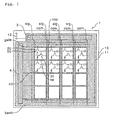
- Fig. 1 is a schematic block diagram of an overall layout of an active matrix display device in accordance with the present invention.
- Fig. 2 is a plan view of one of the pixels extracted included therein.
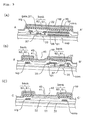
- Figs. 3(A), 3(B) and 3(C) are cross-sectional views taken from line A-A', B-B', and C-C', respectively, in Fig. 2.
- the central portion of a transparent substrate 10 as a base is used as a display section 11.
- a data line driving circuit 3 for outputting image signals is provided on the ends of data lines sig
- a scanning line driving circuit 4 for outputting scanning signals is provided on the ends of scanning lines gate.
- an n-TFT and a p-TFT form a complementary TFT
- many complementary TFTs form a shift resistor circuit, a level shifter circuit, and an analog switch circuit.
- a plurality of scanning lines gate, a plurality of data lines sig extending perpendicular to the extending direction of the scanning lines gate , and a plurality of pixels 7 formed in a matrix by the data lines sig and the scanning lines gate are provided on the transparent substrate 10.
- Each pixel 7 is provided with a conduction control circuit 50 for supplying scanning signals through a scanning line gate , and a thin film luminescent device 40 emitting light on the basis of image signals supplied from a data line sig through the conduction control circuit 50.
- the conduction control circuit 50 includes a first TFT 20 for supplying a scanning signal to a gate electrode through a scanning line gate, a holding capacitor cap for holding an image signal supplied from a data line sig through the first TFT 20, and a second TFT 30 for supplying the image signal held in the holding capacitor cap to the gate electrode.
- the second TFT 30 and the thin film luminescent device 40 are connected in series between an opposite electrode op and a common feed line com .
- the holding capacitor cap may be formed between the opposite electrode op and the scanning line gate , in addition to between the opposite electrode op and the common feed line com .
- the first TFT 20 and the second TFT 30 are formed using islands of semiconductive films (silicon films).
- a gate electrode 21 is formed as a part of the scanning line gate.
- one of the source and drain regions is electrically connected to the data line sig via a contact hole in a first insulating film 51, whereas the other is electrically connected to a drain electrode 22.
- the drain electrode 22 extends towards the region of the second TFT 30, and the extended section is electrically connected to a gate electrode 31 of the second TFT 30 via a contact hole in the first insulating film 51.
- One of the source and drain regions of the second TFT 30 is electrically connected to a relay electrode 35 simultaneously formed with the data line sig via a contact hole in the first insulating film 51, and the relay electrode 35 is electrically connected to a transparent pixel electrode 41 composed of an indium tin oxide (ITO) film in the thin film luminescent device 40 via a contact hole in a second insulating film 52.
- ITO indium tin oxide
- pixel electrodes 41 are independently formed in individual pixels 7.
- An organic semiconductive film 43 composed of polyphenylene vinylene (PPV) or the like and an opposite electrode op composed of a metal film such as lithium-containing aluminum or calcium are deposited above each pixel electrode 41, in that order, to form a thin film luminescent device 40.
- a stripe organic semiconductive film 43 will be formed over a plurality of pixels 7 in some cases, as will be described below.
- the opposite electrode op is formed over the entire display section 11, other than the periphery of the region in which terminals 12 are formed.
- the terminals 12 include a terminal electrically connected to the opposite electrode op formed using a conduction (not shown in the drawing) which is simultaneously formed with the opposite electrode op .
- the configuration of the thin film luminescent device 40 may be a configuration provided with a positive hole injection layer having an increased luminescent efficiency (hole injection efficiency), or a configuration provided with a positive hole injection layer and an electron injection layer.
- the other of the source and drain regions of the second TFT 30 is electrically connected to the common feed line com via a contact hole of the first insulating film 51.
- the extension 39 of the common feed line com faces the extension 36 of the gate electrode 31 separated by the first insulating film 51 as a dielectric film to form a holding capacitor cap.
- a capacitor line formed parallel to the scanning line gate may be used for the formation of the holding capacitor cap.
- the holding capacitor cap may be formed of the drain region of the first TFT 20 and the gate electrode 31 of the second TFT 30.
- the luminescent device 40 emits light as an electroluminescent device or an LED device.
- an insulating film (a bank layer bank, the region shaded with lines slanting downward to the left or double slanting lines at a wide pitch) which is thicker than the organic semiconductive film 41 is provided along the data line sig and the scanning line gate, and the opposite electrode op is formed above the bank layer bank. Since the second insulating film 52 and the thick bank layer bank are disposed between the data line sig and the opposite electrode op, the parasitic capacitance formed in the data line sig is significantly reduced. Thus, the load on the driving circuits 3 and 4 can be reduced, resulting in lower electrical power consumption and improved display operation.
- the bank layer bank consists of a lower insulating layer 61 which is formed of an inorganic material such as a silicon oxide film or a silicon nitride film and is thicker than the organic semiconductive film 41, and an upper insulating layer 62 which is formed on the lower insulating layer 61 and is composed of an organic material such as a resist or a polyimide film.
- the thicknesses of the organic semiconductive film 41, the lower insulating layer 61, and the upper insulating layer 62 are in ranges of 0.05 ⁇ m to 0.2 ⁇ m, 0.2 ⁇ m to 1.0 ⁇ m, and 1 ⁇ m to 2 ⁇ m, respectively.
- the upper insulating layer 62 is formed of a resist or a polyimide film which facilitates formation of a thick film; hence, only the lower insulating layer 61 can be formed of an inorganic material. Since the entire bank layer bank is not formed of an inorganic material, the formation of the inorganic film by, for example, a PECVD process does not require a long time. Thus, productivity of the active matrix display device 1 is increased.
- the organic semiconductive film 41 comes into contact with the inorganic lower insulating layer 61, but not with the organic upper insulating layer 62.
- the organic semiconductive film 41 is, therefore, not damaged by the effects of the organic upper insulating layer 62, and the thin film luminescent device 40 does not have decreased luminescent efficiency nor decreased reliability.
- the bank layer bank is also formed in the peripheral region of the transparent substrate 10 (the exterior region of the display section 11); hence the data line driving circuit 3 and the scanning line driving circuit 4 are covered with the bank layer bank .
- the opposite electrode op must be formed at least in the display section 11, but is unnecessary in the driving circuit region. Since the opposite electrode op is generally formed by a mask sputtering process, an inaccurate alignment such as overlap of the opposite electrode op and the driving circuits may occur.
- the bank layer bank is disposed between the lead layer of the driving circuits and the opposite electrode op ; hence formation of parasitic capacitance in the driving circuits 3 and 4 is prevented even if the opposite electrode op overlaps the driving circuits. As a result, the load on the driving circuits 3 and 4 is reduced, consumption of electrical power is reduced, and high-speed display operation is achieved.
- the bank layer bank is also formed in the area, which overlaps the relay electrode 35 of the conduction control circuit 50, in the region for forming the pixel electrode 41.
- the organic semiconductive film 43 is, therefore, not formed in the area overlapping the relay electrode 35. Since the organic semiconductive film 43 is formed only at the flat section in the region for forming the pixel electrode 41, the resulting organic semiconductive film 43 has a constant thickness so that irregularities of display do not occur. If the organic semiconductive film 43 has a part having a lesser thickness, the driving current for the thin film luminescent device 40 is concentrated therein, resulting in decreased reliability of the thin film luminescent device 40. The uniform thickness in this embodiment does not cause such a problem.
- the organic semiconductive film 43 emits light by a driving current between the relay electrode 35 and the opposite electrode op ; however, the relay electrode 35 and the opposite electrode op inhibit emission of the light to the exterior, and the light does not contribute to display.
- the driving current flowing in the section which does not contribute to display is an unavailable current in view of the display.
- the bank layer bank is formed at the position in which an unavailable current will flow so as to prevent an unavailable current flowing in the common feed line com .
- the width of the common feed line com can be reduced.
- the luminescent area which contributes to improved display performance, such as luminance and contrast, can be increased.
- the bank layer bank When the bank layer bank is formed of a black resist, the bank layer bank functions as a black matrix which improves the quality of display, such as contrast.
- the opposite electrode op is formed on the entire pixel 7 at the front face of the transparent substrate 10; hence light reflected by the opposite electrode op causes decreased contrast.
- the bank layer bank for preventing the formation of the parasitic capacitance is formed of a black resist, the bank layer bank also functions as a black matrix which shades the light reflected by the opposite electrode op and contributes to high contrast.
- the layer can prevent bleeding of a discharged solution outside when the organic semiconductive film 43 is formed by discharging a liquid material (discharging solution) through an ink-jet head in the production process of the active matrix display device.
- the steps for making the first TFT 20 and the second TFT 30 on the transparent substrate 10 are substantially the same as the steps for making the active matrix substrate of the active matrix liquid crystal display device; hence only the outline thereof will be briefly described with reference to Figs. 3(A), 3(B), and 3(C).
- an underlying protective film (not shown in the drawing) composed of a silicon oxide film with a thickness of approximately 2,000 to 5,000 angstroms is formed, if necessary, on a transparent substrate 10 by a plasma enhanced CVD using tetraethoxysilane (TEOS) and gaseous oxygen as formation gases.
- TEOS tetraethoxysilane
- a semiconductive film composed of an amorphous silicon film with a thickness of approximately 300 to 700 angstroms is formed on the underlying protective film by a plasma enhanced CVD.
- the amorphous silicon semiconductive film is subjected to a crystallization step, such as a laser annealing step or a solid phase deposition step so that the semiconductive film is crystallized to form a polysilicon film.
- the semiconductive film is patterned to form islands of semiconductive films, and then a gate insulating film 57 composed of a silicon oxide or silicon nitride film with a thickness of approximately 600 to 1,500 angstroms is formed thereon by a plasma enhanced CVD using tetraethoxysilane (TEOS), gaseous oxygen and the like as formation gases.
- TEOS tetraethoxysilane
- a conductive film composed of a metal film, such as aluminum, tantalum, molybdenum, titanium, or tungsten, is formed by a sputtering process, and is patterned to form gate electrodes 21 and 31 and an extension 36 of the gate electrode 31 (a gate electrode forming step). This step also forms a scanning line gate .
- a metal film such as aluminum, tantalum, molybdenum, titanium, or tungsten
- a high concentration of phosphorus ions are implanted to form source and drain regions by self-alignment with respect to the gate electrodes 21 and 31.
- the section which is not doped with the impurity functions as a channel region.
- a data line sig After forming a first insulating interlayer 51 and then forming contact holes, a data line sig , a drain electrode 22, a common feed line com , an extension 39 of the common feed line com , and a relay electrode 35 are formed. As a result, a first TFT 20, a second TFT 30, and a holding capacitor cap are formed.
- a second insulating interlayer 52 is formed and a contact hole is formed at the position corresponding to the relay electrode 35 of the insulating interlayer.
- An ITO film is formed on the entire second insulating interlayer 52 and is patterned, and then a pixel electrode 41 which is electrically connected to the source and drain regions of the second TFT 30 via the contact hole is formed in each pixel 7.
- An inorganic film (for forming a lower insulating layer 61) is formed on the front face of the second insulating film 52 by a PECVD process, and then a resist (upper insulating layer 62) is formed along the scanning line gate and the data line sig.
- the inorganic film is patterned through the resist as a mask to form a lower insulating layer 61. Since the lower insulating layer 61 is thin, overetching does not occur when the lower insulating layer 61 is formed by such a patterning process. Thus, the pixel electrode 41 is not damaged.
- the inorganic film forms the lower insulating layer 61 along the scanning line gate and the data line sig.
- a double-layered bank layer bank including the lower insulating layer 61 and the upper insulating layer 62 is formed.
- the resist section remaining along the data line sig has a large width so as to cover the common feed line com .
- a region for forming the organic semiconductive film 43 in the luminescent device 40 is surrounded with the bank layer bank .
- Organic semiconductive films 43 corresponding to R, G, and B are formed in regions in a matrix delimited by the bank layer bank by an ink-jet process.
- a liquid material (a precursor or a discharging solution) for forming the organic semiconductive film 43 is discharged in the inner region of the bank layer bank through an ink-jet head and fixed in the inner region of the bank layer bank to form the organic semiconductive film 43.
- the upper insulating layer 62 of the bank layer bank is composed of a resist or a polyimide film, it has water-repellent properties.
- the precursor of the organic semiconductive film 43 contains a hydrophilic solution; hence, the region for forming the organic semiconductive film 43 is surely defined by the bank layer bank . Since the solution does not bleed out of the adjacent pixels 7, the organic semiconductive film 43 can be formed only in the predetermined region.
- the bank layer must have a thickness of approximately 1 ⁇ m to 3 ⁇ m.
- the solvent in the precursor is removed by heat treatment at 100°C to 150°C.
- the thickness of the organic semiconductive film 43 in the inner region of the bank layer bank is fixed in a range of approximately 0.05 ⁇ m to 0.2 ⁇ m. The organic semiconductive film 43 no longer is in contact with the upper insulating layer 62.
- the bank layer bank When the bank layer bank has a height of 1' ⁇ m or more, the bank layer bank sufficiently functions as a barrier even if the bank layer bank does not have water-repellent properties.
- Such a thick bank layer bank can define the region for forming the organic semiconductive film 43 when the film is formed by a coating process in place of the ink-jet process.
- an opposite electrode op is formed on substantially the entire transparent substrate 10.
- organic semiconductive films 43 can be formed at predetermined positions corresponding to R, G, and B by an ink-jet process; hence a full color active matrix display device 1 can be made with high productivity.
- TFTs are also formed in the data line driving circuit 3 and the scanning line driving circuit 4 shown in Fig. 1, these TFTs can be formed by completely or partly employing the above steps for forming the TFT in the pixel 7.
- the TFTs in the driving circuits are also formed in the same interlayer in which TFTs for pixels 7 are formed.
- combinations of an n-type and an n-type, of a p-type and a p-type, and of an n-type and a p-type are allowable. Since all the combinations of TFTs can be produced by any well-known method, description thereof will be omitted.
- Figs. 4(A), 4(B) and 4(C) are cross-sectional views of an active matrix display device in accordance with this embodiment at positions corresponding to line A-A', B-B', and C-C', respectively, in Fig. 2.
- This embodiment has a basic configuration which is substantially the same as that of the first embodiment; hence, the same symbols are assigned for the same parts, without detailed description thereof. Since the region for forming the bank layer bank in the active matrix display device of this embodiment is the same as that in the first embodiment, Figs. 1 and 2 are also referred to in the following description.
- an insulating film (a bank layer bank , the region shaded with lines slanting downward to the left or double slanting lines at a wide pitch) which is thicker than an organic semiconductive film 41 is provided along the data line sig and a scanning line gate , and an opposite electrode op is formed above the bank layer bank .
- the bank layer bank consists of an inorganic lower insulating layer 61 such as a silicon oxide or silicon nitride film which is thicker than the organic semiconductive film 41, and an upper organic insulating film 62 such as a resist or a polyimide film formed on the lower insulating layer 61.
- an inorganic lower insulating layer 61 such as a silicon oxide or silicon nitride film which is thicker than the organic semiconductive film 41
- an upper organic insulating film 62 such as a resist or a polyimide film formed on the lower insulating layer 61.
- the upper organic insulating film 62 has a smaller width than that of the lower inorganic insulating film 61 and is formed on the inner region of the lower insulating layer 61.
- the overlapping width of the upper insulating layer 62 and the pixel electrode 41 is in a range of 1 ⁇ m to 3 ⁇ m
- a gap between an edge of the lower insulating layer 61 and the corresponding edge of the upper insulating layer 62 is in a range of 1 ⁇ m to 5 ⁇ m.
- the bank layer bank has a double-layered configuration in which the underlying insulating film 61 and the upper insulating layer 62 having different widths are deposited.
- the upper insulating layer 62 is formed of a resist or a polyimide film, which facilitates formation of a thick film, in such a double-layered configuration, and only the lower insulating layer 61 is composed of an inorganic material.
- the process, such as a PECVD process, for forming the inorganic film does not require a long deposition time, unlike the process for forming a thick bank layer bank which is entirely composed of an inorganic material.
- the active matrix display device 1 can be manufactured with high productivity.
- the organic semiconductive film 41 comes into contact with the lower insulating layer 61, but not with the upper insulating layer 62. Furthermore, the upper insulating layer 62 is formed on the inner portion of the lower insulating layer 61 to avoid the contact of the organic semiconductive film 43 with the upper insulating layer 62. Thus, the upper organic insulating film 62 does not cause deterioration of the organic semiconductive film 41 which would result in decreased luminescent efficiency and decreased reliability of the thin film luminescent device 40.
- Each pixel 7 is surrounded with the bank layer bank.
- Organic semiconductive films 43 can be formed in predetermined positions corresponding to R, G, and B by an ink-jet process; hence, a full color active matrix display device 1 can be manufactured with high productivity, as in the first embodiment.
- an inorganic film for forming a lower insulating layer 61
- the lower insulating layer 61 is formed along the scanning line gate and the data line sig , and then a resist used for the patterning is removed.
- a resist or a polyimide film with a thickness which is smaller than that of the lower insulating layer 61 is formed thereon as the upper insulating layer 62. Since the lower insulating layer 61 is thin, overetching does not occur when the lower insulating layer 61 is formed by patterning. Thus, the pixel electrode 41 is not damaged.
- An active matrix display device 1 in this embodiment has the same configuration as that in the second embodiment, but a material for the bank layer bank is different. Thus, the same symbols are assigned for the same parts, without detailed description thereof. Figs. 1, 2, and 4 are also referred to in the following description, as in the second embodiment.
- an insulating film (a bank layer bank , the region shaded with lines slanting downward to the left or double slanting lines at a wide pitch) which is thicker than an organic semiconductive film 41 is provided along the data line sig and a scanning line gate , and an opposite electrode op is formed above the bank layer bank .
- the bank layer bank consists of an inorganic lower insulating layer 61 such as a silicon nitride film which is thicker than the organic semiconductive film 41, and an upper inorganic insulating film 62 such as a silicon oxide film formed on the lower insulating layer 61. Since the organic semiconductive film 43 does not come into contact with any other organic material in such a double-layered configuration, it will not be deteriorate by the effects of the other organic material. Thus, a decrease in luminescent efficiency and reliability does not occur in the thin film luminescent device 40.
- the upper organic insulating film 62 has a smaller width than that of the lower inorganic insulating film 61 and is formed on the inner region of the lower insulating layer 61.
- the bank layer bank has a double-layered configuration in which the underlying insulating film 61 and the upper insulating layer 62 having different widths are deposited.
- inorganic films for forming the lower insulating layer 61 and the upper insulating layer 62 are formed in that order, and the upper insulating layer 62 is patterned. Since the lower insulating layer 61 functions as an etching stopper, slight overetching will not damage the pixel electrode 41. After the patterning, the lower insulating layer 61 is patterned. Since a single layer of the lower insulating layer 61 is etched, the etching is readily controlled and overetching which would damage the pixel electrode 41 does not occur.
- Each pixel 7 is, therefore, surrounded with the bank layer bank .
- Organic semiconductive films 43 can be formed in predetermined positions corresponding to R, G, and B by an ink-jet process; hence, a full color active matrix display device 1 can be manufactured with high productivity, as in the first embodiment.
- the bank layer bank delimits pixels 7 in a matrix.
- the bank layer bank may be formed along only the data line sig .
- Organic semiconductive film 43 having a striped pattern, corresponding to R, G, and B, can be formed in striped regions delimited by the bank layer bank by an ink-jet process; hence a full color active matrix display device 1 can be made with high productivity.
- the corners delimited by the bank layer bank are edged in the above embodiments, it may be rounded so that the organic semiconductive film 43 has a rounded planar shape.
- the organic semiconductive film 43 having such a shape avoids the concentration of the driving current at the corners, hence defects, such as insufficient voltage resistance, can be prevented at the corners.
- An active matrix display device 1 in this embodiment has a basic configuration like that in the first, second or third embodiment; hence, Fig. 1 is referred to for the description, and the same symbols are assigned for the same parts, without detailed description thereof.
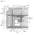
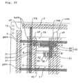
- Fig. 5 is a plan view of a pixel taken from an active matrix display device of this embodiment.
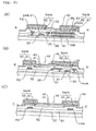
- Figs. 6(A), 6(B) and 6(C) are cross-sectional views taken from line A-A', B-B', and C-C', respectively, in Fig. 5.
- an upper insulating layer 62 partly overlaps a lower insulating layer 61 in this embodiment so that these films have different functions.
- a plurality of scanning lines gate a plurality of data lines sig extending perpendicular to the extending direction of the scanning lines gate , a plurality of common feed lines com formed parallel to the data lines sig , and a plurality of pixels 7 formed in a matrix by the data lines sig and the scanning lines gate are provided.
- a lower insulating layer 61 (a region shaded by double lines slanting down toward the left) is formed so as to cover an area overlapping the portion for forming a conduction control circuit 50 in the region for forming a pixel electrode 41; the data line sig ; the common feed line com ; and the scanning line gate .
- the upper insulating layer 62 (a region shaded by lines at a wide pitch and slanting down toward the left) is formed only on areas along the data lines sig in the region for forming the lower insulating layer 61 so as to form a striped pattern.
- Organic semiconductive films 43 are formed in the striped areas delimited by the upper insulating layer 62.
- the overlapping section of the lower insulating layer 61 and the upper insulating layer 62 is used as a bank layer bank to prevent bleeding of the discharged solution.
- the overlapping section of the lower insulating layer 61 and the upper insulating layer 62 has a thickness of 1 ⁇ m or more.
- the second insulating film 52 and the thick bank layer bank are disposed between the data lines sig and the opposite electrode op in such a configuration, parasitic capacitance forming in the data line sig is significantly reduced.
- the load on the driving circuits 3 and 4 can be reduced, resulting in lower electrical power consumption and improved display operation.
- the striped organic semiconductive films 43 are formed, an area overlapping the portion for forming a conduction control circuit 50 in the region for forming the pixel electrode 41, and a scanning line gate are covered with the upper insulating layer 62.
- organic semiconductive film 43 formed only on the flat section in the pixel electrode 41 contributes to luminescence.
- the thin film luminescent device 40 is formed only in the flat section of the pixel electrode 41.
- the organic semiconductive film 43 has a constant thickness and does not cause irregularities of display and concentration of a driving current. Since the lower insulating layer 61 inhibits a current flow in the section which does not contribute to display, an unavailable current does not flow in the common feed line com .
- the underlying insulating film 61 is formed of an inorganic material such as a silicon oxide film or a silicon nitride film which is thicker than the organic semiconductive film 41 and when the upper insulating layer 62 is composed of an organic material such as a resist or a polyimide film, only the lower insulating layer 61 is composed of the inorganic material.
- the process, such as a PECVD process, for forming the inorganic film does not require a long deposition time, unlike the process for forming a thick bank layer bank which is entirely composed of an inorganic material.
- the active matrix display device 1 can be manufactured with high productivity.
- the organic semiconductive film 41 comes into contact with the lower insulating layer 61, but not with the upper organic insulating film 62.
- the upper organic insulating film 62 does not cause deterioration of the organic semiconductive film 41 which results in decreased luminescent efficiency and decreased reliability of the thin film luminescent device 40.
- the organic semiconductive film 43 does not come into contact with an organic material and thus is not deteriorated by the effects of the organic material. Thus, a decrease in the luminescent efficiency and reliability does not occur in the thin film luminescent device 40.
- the lower insulating layer 61 functions as an etching stopper when the upper insulating layer 62 is patterned, as described in the third embodiment.
- Fig. 7 is a schematic block diagram of an overall layout of an active matrix display device.
- Fig. 8 is a plan view of a pixel extracted therefrom.
- Figs. 9(A), 9(B) and 9(C) are cross-sectional views taken from line A-A', B-B', and C-C', respectively, in Fig. 8.
- This embodiment has a basic configuration which is substantially the same as that of the first embodiment; hence, the same symbols are assigned for the same parts, without detailed description thereof.
- an insulating film (a bank layer bank , the region shaded with lines slanting downward to the left or double slanting lines at a wide pitch) which is thicker than an organic semiconductive film 41 is provided along the data line sig and a scanning line gate , and an opposite electrode op is formed above the bank layer bank . Since the second insulating film 52 and the thick bank layer bank are disposed between the data lines sig and the opposite electrode op , parasitic capacitance forming in the data line sig is significantly reduced. Thus, the load on the driving circuits 3 and 4 can be reduced, resulting in lower electrical power consumption and improved display operation.
- the bank layer bank consists of a lower insulating layer 61 which is formed of an inorganic material such as a silicon oxide film or a silicon nitride film and is thicker than the organic semiconductive film 41, and an upper insulating layer 62 which is formed on the lower insulating layer 61 and is composed of an organic material such as a resist or a polyimide film.
- the thicknesses of the organic semiconductive film 41, the lower insulating layer 61, and the upper insulating layer 62 are in ranges of 0.05 ⁇ m to 0.2 ⁇ m, 0.2 ⁇ m to 1.0 ⁇ m, and 1 ⁇ m to 2 ⁇ m, respectively.
- the organic semiconductive film 41 comes into contact with the inorganic lower insulating layer 61, but not with the organic upper insulating layer 62.
- the organic semiconductive film 41 is, therefore, not damaged by the effects of the organic upper insulating layer 62, and the thin film luminescent device 40, as in the first embodiment, does not have decreased luminescent efficiency nor decreased reliability.
- discontinuities portion off are provided for both the lower insulating layer 61 and the upper insulating layer 62 of the bank layer bank along the data lines sig between adjacent pixels 7.
- discontinuities portion off are also provided for both the lower insulating layer 61 and the upper insulating layer 62 of the bank layer bank along the scanning lines gate between adjacent pixels 7.
- discontinuities portion off are provided for both the lower insulating layer 61 and the upper insulating layer 62 of the bank layer bank at the ends of each data line sig and each scanning line gate .
- the thick bank layer bank is not provided at each discontinuity off , the discontinuity off does not have a large step and is flat. Thus, the opposite electrode op formed at this section does not cause disconnection.
- the opposite electrodes op of adjacent pixels 7 are securely connected through the flat section not having a step of the bank layer bank . Accordingly, a thick insulating film (a bank layer bank ) can be formed around a pixel 7 to suppress the parasitic capacitance, without disconnection of the opposite electrodes op formed on the thick insulating film (bank layer bank ).
- the data line driving circuit 3 and the scanning line driving circuit 4 are covered with the bank layer bank (the region is indicated by shading).
- the opposite electrode op provided above the region for forming these driving circuits is separated by the bank layer bank from the lead layer of these driving circuits. Since formation of the parasitic capacitance in the driving circuits can be prevented, the load on the driving circuits 3 and 4 can be reduced, resulting in lower electrical power consumption and improved display operation.
- a discontinuity off (second discontinuity) is provided for both the lower insulating layer 61 and the upper insulating layer 62 of the bank layer bank between the region for forming the scanning line driving circuit 4 and the region for the data line driving circuit 3.
- the opposite electrode op at the side of the display section 11 and the opposite electrode op at the peripheral side of the substrate are connected through the discontinuity off of the bank layer bank , and the discontinuity off is also a flat section not having a step. Since the opposite electrode op formed at the discontinuity off does not cause disconnection, the opposite electrodes op of the display section 11 and the opposite electrode op of the peripheral section of the substrate are securely connected through the discontinuity off of the bank layer bank . Thus, terminals 12 connected to the opposite electrode op of the peripheral section of the substrate are securely connected to the opposite electrode op of the display section 11.
- the bank layer bank is also formed in an area in which the region for forming the pixel electrode 41 overlaps the relay electrode 35 of the conduction control circuit 50 in this embodiment, no unavailable current flows. Accordingly, the width of the common feed line com can be reduced.
- the bank layer bank is formed on the front face of the second insulating film 52 along the scanning lines gate and the data lines sig , as in the first embodiment. Discontinuities portion off are formed at predetermined positions of the bank layer bank .
- the bank layer bank formed along the data lines sig has a larger width so that it can cover the common feed line com . As a result, the region for forming the organic semiconductive film 43 in the thin film luminescent device 40 is surrounded with the bank layer bank .
- Organic semiconductive films 43 corresponding to R, G, and B are formed in a region delimited as a matrix by the bank layer bank by an ink-jet process.
- a liquid material (a precursor) for forming the organic semiconductive film 43 is discharged into the inner region of the bank layer bank through an ink-jet head and is fixed in the inner region of the bank layer bank to form the organic semiconductive film 43.
- the upper insulating layer 62 of the bank layer bank is composed of a resist or a polyimide film, it has water-repellent properties.
- the precursor of the organic semiconductive film 43 contains a hydrophilic solution; hence, the region for forming the organic semiconductive film 43 is surely defined by the bank layer bank , and the solution does not bleed out of the adjacent pixels 7.
- the region for forming the organic semiconductive film 43 can be surely defined by the bank layer bank , and the solution does not bleed out into adjacent pixels 7. Accordingly, the organic semiconductive film 43 can be formed within a predetermined region.
- the bank layer Since the precursor discharged from the ink-jet head forms a convex surface with a thickness of approximately 2 ⁇ m to 4 ⁇ m by surface tension, the bank layer must have a thickness of approximately 1 ⁇ m to 3 ⁇ m. Although the precursor discharged from the ink-jet head comes into contact with the upper insulating layer 62 in this state, the solvent in the precursor is removed by heat treatment at 100°C to 150°C. Thus, the thickness of the organic semiconductive film 43 fixed in the inner region of the bank layer bank is in a range of approximately 0.05 ⁇ m to 0.2 ⁇ m. The organic semiconductive film 43 no longer is in contact with the upper insulating layer 62.
- the bank layer bank When the bank layer bank has a height of 1 ⁇ m or more, the bank layer bank sufficiently functions as a barrier even if the bank layer bank does not have water-repellent properties.
- Such a thick bank layer bank can define the region for forming the organic semiconductive film 43 when the film is formed by a coating process in place of the ink-jet process.
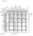
- Fig. 10 is a schematic block diagram of an overall layout of an active matrix display device.
- Fig. 11 is a plan view of a pixel taken from the device.
- Figs. 12(A), 12(B) and 12(C) are cross-sectional views taken from line A-A', B-B', and C-C', respectively, in Fig. 11.
- This embodiment has a basic configuration which is substantially the same as that of the first embodiment; hence, the same symbols are assigned for the same parts, without detailed description thereof.
- an insulating film (a bank layer bank , the region shaded with lines slanting downward to the left or double slanting lines at a wide pitch) which is thicker than an organic semiconductive film 43 is provided along the data line sig and a scanning line gate , and an opposite electrode op is formed above the bank layer bank . Since the second insulating film 52 and the thick bank layer bank are disposed between the data lines sig and the opposite electrode op , parasitic capacitance forming in the data line sig is significantly reduced. Thus, the load on the driving circuits 3 and 4 can be reduced, resulting in lower electrical power consumption and improved display operation.
- the bank layer bank consists of a lower insulating layer 61 which is formed of an inorganic material such as a silicon oxide film or a silicon nitride film and is thicker than the organic semiconductive film 43, and an upper insulating layer 62 which is formed on the lower insulating layer 61 and is composed of an organic material such as a resist or a polyimide film.
- the organic semiconductive film 43 comes into contact with the inorganic lower insulating layer 61, but not with the organic upper insulating layer 62.
- the organic semiconductive film 43 is, therefore, not damaged by the effects of the organic upper insulating layer 62, and the thin film luminescent device 40, as in the first embodiment, does not decreased luminescent efficiency nor decreased reliability.
- the bank layer bank is formed along the data line sig and the scanning line gate and each pixel 7 is surrounded with the bank layer bank .
- Organic semiconductive films 43 can be formed in predetermined positions corresponding to R, G, and B by an ink-jet process; hence, a full color active matrix display device 1 can be manufactured with high productivity.
- discontinuities portion off are provided for the bank layer bank along the scanning line gate between adjacent pixels 7.
- discontinuities portion off are also provided for the bank layer bank at the ends of each data line sig and each scanning line gate .
- a discontinuity off is provided for the bank layer bank between the region for forming the scanning line driving circuit 4 and the region for the data line driving circuit 3.
- Fig. 13 is a schematic block diagram of an overall layout of an active matrix display device.
- Fig. 14 is a plan view of a pixel taken from the device.
- Figs. 15(A) 15(B) and 15(C) are cross-sectional views taken from line A-A', B-B', and C-C', respectively, in Fig. 14.
- This embodiment has a basic configuration which is substantially the same as that of the first embodiment; hence, the same symbols are assigned for the same parts, without detailed description thereof.
- an insulating film (a bank layer bank , the region shaded with lines slanting downward to the left or double slanting lines at a wide pitch) which is thicker than an organic semiconductive film 43 is provided along the data line sig and a scanning line gate , and an opposite electrode op is formed above the bank layer bank . Since the second insulating film 52 and the thick bank layer bank are disposed between the data lines sig and the opposite electrode op , parasitic capacitance forming in the data line sig is significantly reduced. Thus, the load on the driving circuits 3 and 4 can be reduced, resulting in lower electrical power consumption and improved display operation.
- the bank layer bank consists of a lower insulating layer 61 which is formed of an inorganic material such as a silicon oxide film or a silicon nitride film and is thicker than the organic semiconductive film 43, and an upper insulating layer 62 which is formed on the lower insulating layer 61 and is composed of an organic material such as a resist or a polyimide film.
- the organic semiconductive film 43 comes into contact with the inorganic lower insulating layer 61, but not with the organic upper insulating layer 62.
- the organic semiconductive film 43 is, therefore, not damaged by the effects of the organic upper insulating layer 62, and the thin film luminescent device 40, as in the first embodiment, does not have decreased luminescent efficiency nor decreased reliability.
- the bank layer bank is formed along the data line sig and the scanning line gate and each pixel 7 is surrounded with the bank layer bank .
- Organic semiconductive films 43 can be formed in predetermined positions corresponding to R, G, and B by an ink-jet process; hence, a full color active matrix display device 1 can be manufactured with high productivity.
- discontinuities portion off are provided for the bank layer bank along the data line sig between adjacent pixels 7.
- discontinuities portion off are also provided for the bank layer bank at the ends of each data line sig and each scanning line gate .
- a discontinuity off is provided for the bank layer bank between the region for forming the scanning line driving circuit 4 and the region for the data line driving circuit 3.
- Fig. 16 is a schematic block diagram of an overall layout of an active matrix display device.
- Fig. 17 is a plan view of a pixel taken from the device.
- Figs. 18(A), 18(B), and 18(C) are cross-sectional views taken from line A-A', B-B', and C-C', respectively, in Fig. 17.
- This embodiment has a basic configuration which is substantially the same as that of the first and fifth embodiments; hence, the same symbols are assigned for the same parts, without detailed description thereof.
- an insulating film (a bank layer bank , the region shaded with lines slanting downward to the left or double slanting lines at a wide pitch) which is thicker than an organic semiconductive film 43 is provided along the data line sig and a scanning line gate , and an opposite electrode op is formed above the bank layer bank . Since the second insulating film 52 and the thick bank layer bank are disposed between the data lines sig and the opposite electrode op , parasitic capacitance forming in the data line sig is significantly reduced. Thus, the load on the driving circuits 3 and 4 can be reduced, resulting in lower electrical power consumption and improved display operation.
- the bank layer bank consists of a lower insulating layer 61 which is formed of an inorganic material such as a silicon oxide film or a silicon nitride film and is thicker than the organic semiconductive film 43, and an upper insulating layer 62 which is formed on the lower insulating layer 61 and is composed of an organic material such as a resist or a polyimide film.
- the bank layer bank is formed along the data line sig and the scanning line gate and each pixel 7 is surrounded with the bank layer bank .
- Organic semiconductive films 43 can be formed in predetermined positions corresponding to R, G, and B by an ink-jet process; hence, a full color active matrix display device 1 can be manufactured with high productivity.
- discontinuities portion off are provided for the bank layer bank along the data line sig between adjacent pixels 7.
- discontinuities portion off are also provided for the bank layer bank at the ends of each data line sig and each scanning line gate .
- a discontinuity off is provided for the bank layer bank between the region for forming the scanning line driving circuit 4 and the region for the data line driving circuit 3.
- these discontinuities portion off are provided for only the upper insulating layer 62 between the lower insulating layer 61 (a region shaded by double slashes) and the upper insulating layer 62 (a region shaded by lines slanting down to the left) of the bank layer bank , and thus the lower insulating layer 61 is formed at the discontinuities portion off .
- the lower insulating layer 61 is formed for the first and second discontinuities portion in this embodiment, the present invention is not limited to this embodiment.
- the lower insulating layer 61 may be formed for either the first discontinuities portion or the second discontinuity.
- the configuration of this embodiment in which the lower insulating layer 61 is formed at the discontinuities portion can be applied to the bank layer bank having a pattern described in any other embodiment.
- Fig. 19 is a schematic block diagram of an overall layout of an active matrix display device.
- Fig. 20 is a plan view of a pixel taken from the device.
- Figs. 21(A), 21(B) and 21(C) are cross-sectional views taken from line A-A', B-B', and C-C', respectively, in Fig. 20.
- This embodiment has a basic configuration which is substantially the same as that of the first and fifth embodiments; hence, the same symbols are assigned for the same parts, without detailed description thereof.
- an insulating film (a bank layer bank , the region shaded with lines slanting downward to the left or double slanting lines at a wide pitch) which is thicker than an organic semiconductive film 43 is provided along the data line sig and a scanning line gate , and an opposite electrode op is formed above the bank layer bank . Since the second insulating film 52 and the thick bank layer bank are disposed between the data lines sig and the opposite electrode op , parasitic capacitance forming in the data line sig is significantly reduced. Thus, the load on the driving circuits 3 and 4 can be reduced, resulting in lower electrical power consumption and improved display operation.
- the bank layer bank consists of a lower insulating layer 61 which is formed of an inorganic material such as a silicon oxide film or a silicon nitride film and is thicker than the organic semiconductive film 43, and an upper insulating layer 62 which is formed on the lower insulating layer 61 and is composed of an organic material such as a resist or a polyimide film.
- the organic semiconductive film 43 comes into contact with the inorganic lower insulating layer 61, but not with the organic upper insulating layer 62.
- the organic semiconductive film 43 is, therefore, not damaged by the effects of the organic upper insulating layer 62, and the thin film luminescent device 40 does not have decreased luminescent efficiency nor decreased reliability.
- organic semiconductive film 43 having a striped pattern, corresponding to R, G, and B, can be formed in striped regions delimited by the bank layer bank by an ink-jet process; hence a full color active matrix display device 1 can be made with high productivity.
- discontinuities portion off are provided for both the lower insulating layer 61 and the upper insulating layer 62 of the bank layer bank along the data lines sig at the ends of each data line sig.
- the opposite electrode op of each pixel 7 is connected to the opposite electrode op of the adjacent pixel 7 over the thick bank layer bank' in the direction of the scanning line gate .
- the opposite electrode op of each pixel 7 is connected to the opposite electrode op of the adjacent pixel 7 at the discontinuity off (the flat section not having a step due to the bank layer bank ) at the ends of the data line sig . Since the opposite electrode op of each pixel 7 is connected to the opposite electrode op of the adjacent pixel 7 at the flat section not having a step due to the bank layer bank , the opposite electrode op of each pixel 7 does not cause disconnection.
- the data line driving circuit 3 and the scanning line driving circuit 4 are covered with the bank layer bank .
- the opposite electrode op provided above the region for forming these driving circuits is separated by the bank layer bank from the lead layer of these driving circuits. Since formation of the parasitic capacitance in the driving circuits can be prevented, the load on the driving circuits 3 and 4 can be reduced, resulting in lower electrical power consumption and improved display operation.
- the bank layer bank which is formed above the scanning line driving circuit 4 and the data line driving circuit 3, has a discontinuity off (second discontinuity) between the region for forming the scanning line driving circuit 4 and the region for the data line driving circuit 3.
- the opposite electrodes are securely connected through the flat section not having a step due to the bank layer bank (the discontinuity off ) without disconnection.
- the configuration in which only the upper insulating layer 62 has discontinuities portion off of the bank layer bank may also be applied to the sixth embodiment.
- the concept of provision of discontinuities portion off in the bank layer bank for avoiding disconnection of the opposite electrodes op is also applicable to a bank layer bank composed of an inorganic material, as described in the third embodiment.
- the insulating film which is formed so as to surround the region for forming the organic semiconductive film consists of a lower insulating layer which is composed of an inorganic material and is thicker than the organic semiconductive film, and an upper insulating layer which is formed thereon and is composed of an organic material. Since a thick insulating film is disposed between the data line and the opposite electrode, formation of parasitic capacitance in the data line can be prevented. Thus, the load on the data line driving circuit can be reduced, resulting in lower electrical power consumption and improved display operation.
- the process has high productivity.
- the upper insulating layer does not come into contact with the organic semiconductive film, but the lower insulating layer composed of an inorganic material does come into contact with the organic semiconductive film; hence, the organic semiconductive film is protected from deterioration caused by the upper insulating layer. Accordingly, the thin film luminescent device does not have decreased luminescent efficiency or reliability.
- the insulating film formed so as to surround the region for forming the organic semiconductive film consists of a lower insulating layer composed of an inorganic material and an upper insulating layer which is formed on an inner region of the lower insulating layer and has a smaller width than that of the lower insulating layer.
- the thick insulating film disposed between the data line and the opposite electrode can prevent formation of parasitic capacitance in the data line.
- the load on the data line driving circuit can be reduced, resulting in lower electrical power consumption and improved display operation.
- the lower insulating layer functions as an etching stopper.
Landscapes
- Engineering & Computer Science (AREA)
- Microelectronics & Electronic Packaging (AREA)
- Physics & Mathematics (AREA)
- General Physics & Mathematics (AREA)
- Theoretical Computer Science (AREA)
- Optics & Photonics (AREA)
- Electroluminescent Light Sources (AREA)
- Devices For Indicating Variable Information By Combining Individual Elements (AREA)
Claims (19)
- Anzeigevorrichtung mit aktiver Matrix (1), umfassend einen Anzeigebereich mit einer Vielzahl von Abtastleitungen auf einem Substrat (10), einer Vielzahl von Datenleitungen, die sich in die Richtung senkrecht zu der Richtung der Abtastleitungen erstrecken, und einer Vielzahl von Pixeln (7), die in einer Matrix angeordnet sind, die durch die Datenleitungen und die Abtastleitungen begrenzt ist; wobei jedes der Pixel (7) mit einer Dünnfilmleuchtvorrichtung (40) versehen ist, die eine Leitungssteuerschaltung (50) aufweist, die einen Dünnfilmtransistor (20) zum Zuleiten eines Abtastsignals zu einer Gate-Elektrode (21) durch eine der Abtastleitungen enthält, sowie eine Pixelelektrode (41), einen organischen Halbleiterfilm (43), der über der Pixelelektrode (41) abgeschieden ist, und eine Gegenelektrode, die über dem organischen Halbleiterfilm (43) abgeschieden ist; wobei die Dünnfilmleuchtvorrichtung (40) Licht auf der Basis eines Bildsignals ausstrahlt, das von der Datenleitung durch die Leitungssteuerschaltung (50) zugeleitet wird; dadurch gekennzeichnet, dass
der Bereich zur Bildung des organischen Halbleiterfilms (43) durch einen Isolierfilm geteilt ist, der dicker als der organische Halbleiterfilm (43) ist; und
der Isolierfilm eine untere Isolierschicht umfasst, die aus einem anorganischen Material gebildet und dicker als der organische Halbleiterfilm (43) ist, und eine obere Isolierschicht, die auf der unteren Isolierschicht abgeschieden und aus einem organischen Material gebildet ist. - Anzeigevorrichtung mit aktiver Matrix (1) nach Anspruch 1, wobei die obere Isolierschicht in einem inneren Bereich der unteren Isolierschicht so abgeschieden ist, dass sie eine geringere Breite als die untere Isolierschicht hat.
- Anzeigevorrichtung mit aktiver Matrix, umfassend einen Anzeigebereich mit einer Vielzahl von Abtastleitungen auf einem Substrat, einer Vielzahl von Datenleitungen, die sich in die Richtung senkrecht zu der Richtung der Abtastleitungen erstrecken, und einer Vielzahl von Pixeln, die in einer Matrix angeordnet sind, die durch die Datenleitungen und die Abtastleitungen begrenzt ist; wobei jedes der Pixel mit einer Dünnfilmleuchtvorrichtung versehen ist, die eine Leitungssteuerschaltung aufweist, die einen Dünnfilmtransistor zum Zuleiten eines Abtastsignals zu einer Gate-Elektrode durch eine der Abtastleitungen enthält, sowie eine Pixelelektrode, einen organischen Halbleiterfilm, der über der Pixelelektrode abgeschieden ist, und eine Gegenelektrode, die über dem organischen Halbleiterfilm abgeschieden ist; wobei die Dünnfilmleuchtvorrichtung Licht auf der Basis eines Bildsignals ausstrahlt, das von der Datenleitung durch die Leitungssteuerschaltung zugeleitet wird; wobei
der Bereich zur Bildung des organischen Halbleiterfilms durch einen Isolierfilm geteilt ist, der dicker als der organische Halbleiterfilm ist; und
der Isolierfilm eine untere Isolierschicht umfasst, die aus einem anorganischen Material besteht, und eine obere Isolierschicht, die aus einem anorganischen Material besteht, die eine geringere Breite als die untere Isolierschicht hat. - Anzeigevorrichtung mit aktiver Matrix nach einem der Ansprüche 1 bis 3, wobei die Leitungssteuerschaltung mit einem ersten TFT zum Zuleiten des Abtastsignals zu der Gate-Elektrode versehen ist, sowie mit einem zweiten TFT, dessen Gate-Elektrode durch den ersten TFT an die Datenleitung angeschlossen ist; und
der zweite TFT und die Dünnfilmleuchtvorrichtung in Serie zwischen einer allgemeinen Zuleitung, die zusätzlich zu der Datenleitung und der Abtastleitung zum Zuleiten eines Antriebsstroms ausgebildet ist, und der Gegenelektrode angeschlossen sind. - Anzeigevorrichtung mit aktiver Matrix nach einem der Ansprüche 1 bis 4, wobei der Isolierfilm als Bankschicht verwendet wird, die ein Auslaufen einer abgegebenen Lösung verhindert, wenn der organische Halbleiterfilm durch ein Tintenstrahlverfahren in einem Bereich gebildet wird, der durch den Isolierfilm begrenzt ist.
- Anzeigevorrichtung mit aktiver Matrix nach Anspruch 5, wobei der Isolierfilm eine Dicke von 1 µm oder mehr hat.
- Anzeigevorrichtung mit aktiver Matrix nach einem der Ansprüche 1 bis 6, wobei ein Bereich, der die Fläche zur Bildung der Leitungssteuerschaltung in dem Bereich zur Bildung der Pixelelektrode überlappt, mit dem Isolierfilm bedeckt ist.
- Anzeigevorrichtung mit aktiver Matrix nach einem der Ansprüche 1 bis 7, wobei die Ecken, die durch den Isolierfilm begrenzt sind, abgerundet sind.
- Anzeigevorrichtung mit aktiver Matrix nach einem der Ansprüche 1 bis 4, wobei die untere Isolierschicht des Isolierfilms so gebildet ist, dass sie die Fläche zur Bildung der Leitungssteuerschaltung in dem Bereich zur Bildung der Pixelelektrode, der Datenleitung, der allgemeinen Zuleitung und der Abtastleitung überlappt, während die obere Isolierschicht so gebildet ist, dass sie ein gestreiftes Muster entlang der Datenleitung bildet; und
der organische Halbleiterfilm in dem Bereich gebildet ist, der durch das gestreifte Muster der oberen Isolierschicht begrenzt ist. - Anzeigevorrichtung mit aktiver Matrix nach Anspruch 9, wobei der überlappende Abschnitt, in dem die untere Isolierschicht die obere Isolierschicht überlappt, als Bankschicht verwendet wird, die ein Auslaufen einer abgegebenen Lösung verhindert, wenn der leuchtende Dünnfilm durch ein Tintenstrahlverfahren gebildet wird.
- Anzeigevorrichtung mit aktiver Matrix nach Anspruch 10, wobei der überlappende Abschnitt der unteren Isolierschicht und der oberen Isolierschicht eine Dicke von 1 µm oder mehr hat.
- Anzeigevorrichtung mit aktiver Matrix nach einem der Ansprüche 1 bis 11, wobei der Isolierfilm einen ersten Diskontinuitätenabschnitt aufweist, so dass Gegenelektroden benachbarter Pixel an flachen Abschnitten miteinander verbunden sind, die durch den ersten Diskontinuitätenabschnitt gebildet sind.
- Anzeigevorrichtung mit aktiver Matrix nach Anspruch 12, wobei der Isolierfilm entlang der Datenleitung und der Abtastleitung so gebildet ist, dass er den Bereich zur Bildung des organischen Halbleiterfilms umgibt, und der erste Diskontinuitätenabschnitt zwischen den benachbarten Pixeln in die Richtung der verlängerten Datenleitung und die Richtung der verlängerten Abtastleitung gebildet ist.
- Anzeigevorrichtung mit aktiver Matrix nach Anspruch 12, wobei der Isolierfilm entlang der Datenleitung und der Abtastleitung so gebildet ist, dass er den Bereich zur Bildung des organischen Halbleiterfilms umgibt, und der erste Diskontinuitätenabschnitt zwischen den benachbarten Pixeln in die Richtung der verlängerten Abtastleitung gebildet ist.
- Anzeigevorrichtung mit aktiver Matrix nach Anspruch 12, wobei der Isolierfilm entlang der Datenleitung und der Abtastleitung so gebildet ist, dass er den Bereich zur Bildung des organischen Halbleiterfilms umgibt, und der erste Diskontinuitätenabschnitt zwischen den benachbarten Pixeln in die Richtung der verlängerten Datenleitung gebildet ist.
- Anzeigevorrichtung mit aktiver Matrix nach Anspruch 12, wobei sich der Isolierfilm in einem gestreiften Muster entlang der Datenleitung erstreckt und die erste Diskontinuität auf mindestens einem Ende der Verlaufsrichtung gebildet ist.
- Anzeigevorrichtung mit aktiver Matrix nach Anspruch 12, wobei die Peripherie des Anzeigeabschnitts mit einer Datenleitungstreiberschaltung zum Zuleiten von Datensignalen durch die Datenleitungen versehen ist, und einer Abtastleitungstreiberschaltung zum Zuleiten von Abtastsignalen durch die Abtastleitungen,
der Isolierfilm auch über der Abtastleitungstreiberschaltung und der Datenleitungstreiberschaltung gebildet ist, und der Isolierfilm eine zweite Diskontinuität an einer Position zwischen dem Bereich zum Bilden der Abtastleitungstreiberschaltung und dem Bereich zum Bilden der Datenleitungstreiberschaltung aufweist, so dass die Gegenelektroden an dem Anzeigeabschnitt und an dem peripheren Abschnitt des Substrats durch den flachen Abschnitt verbunden sind, der keine Stufe aufweist, die durch den Isolierfilm gebildet wird. - Anzeigevorrichtung mit aktiver Matrix nach einem der Ansprüche 12 bis 17, wobei sowohl die untere Isolierschicht als auch die obere Isolierschicht den Diskontinuitätenabschnitt haben.
- Anzeigevorrichtung mit aktiver Matrix nach einem der Ansprüche 12 bis 17, wobei nur die obere Isolierschicht zwischen der unteren Isolierschicht und der oberen Isolierschicht den Diskontinuitätenabschnitt haben kann.
Priority Applications (1)
| Application Number | Priority Date | Filing Date | Title |
|---|---|---|---|
| EP04078120A EP1505648A3 (de) | 1997-08-21 | 1998-08-20 | Anzeigevorrichtung mit aktiver Matrix |
Applications Claiming Priority (3)
| Application Number | Priority Date | Filing Date | Title |
|---|---|---|---|
| JP22543497 | 1997-08-21 | ||
| JP22543497 | 1997-08-21 | ||
| PCT/JP1998/003699 WO1999010862A1 (en) | 1997-08-21 | 1998-08-20 | Active matrix display |
Related Child Applications (1)
| Application Number | Title | Priority Date | Filing Date |
|---|---|---|---|
| EP04078120A Division EP1505648A3 (de) | 1997-08-21 | 1998-08-20 | Anzeigevorrichtung mit aktiver Matrix |
Publications (3)
| Publication Number | Publication Date |
|---|---|
| EP0940797A1 EP0940797A1 (de) | 1999-09-08 |
| EP0940797A4 EP0940797A4 (de) | 2002-08-21 |
| EP0940797B1 true EP0940797B1 (de) | 2005-03-23 |
Family
ID=16829317
Family Applications (2)
| Application Number | Title | Priority Date | Filing Date |
|---|---|---|---|
| EP04078120A Ceased EP1505648A3 (de) | 1997-08-21 | 1998-08-20 | Anzeigevorrichtung mit aktiver Matrix |
| EP98938919A Expired - Lifetime EP0940797B1 (de) | 1997-08-21 | 1998-08-20 | Anzeigevorrichtung mit aktiver matrix |
Family Applications Before (1)
| Application Number | Title | Priority Date | Filing Date |
|---|---|---|---|
| EP04078120A Ceased EP1505648A3 (de) | 1997-08-21 | 1998-08-20 | Anzeigevorrichtung mit aktiver Matrix |
Country Status (8)
| Country | Link |
|---|---|
| US (5) | US6380672B1 (de) |
| EP (2) | EP1505648A3 (de) |
| JP (1) | JP3536301B2 (de) |
| KR (2) | KR100627091B1 (de) |
| CN (4) | CN1267871C (de) |
| DE (1) | DE69829458T2 (de) |
| TW (1) | TW388855B (de) |
| WO (1) | WO1999010862A1 (de) |
Families Citing this family (149)
| Publication number | Priority date | Publication date | Assignee | Title |
|---|---|---|---|---|
| JP3520396B2 (ja) * | 1997-07-02 | 2004-04-19 | セイコーエプソン株式会社 | アクティブマトリクス基板と表示装置 |
| EP1505648A3 (de) * | 1997-08-21 | 2005-08-10 | Seiko Epson Corporation | Anzeigevorrichtung mit aktiver Matrix |
| JP3580092B2 (ja) * | 1997-08-21 | 2004-10-20 | セイコーエプソン株式会社 | アクティブマトリクス型表示装置 |
| JP3804646B2 (ja) * | 1997-08-21 | 2006-08-02 | セイコーエプソン株式会社 | 表示装置 |
| JP3646510B2 (ja) * | 1998-03-18 | 2005-05-11 | セイコーエプソン株式会社 | 薄膜形成方法、表示装置およびカラーフィルタ |
| JP4298131B2 (ja) | 1999-05-14 | 2009-07-15 | 株式会社半導体エネルギー研究所 | 液晶表示装置の作製方法 |
| US7288420B1 (en) * | 1999-06-04 | 2007-10-30 | Semiconductor Energy Laboratory Co., Ltd. | Method for manufacturing an electro-optical device |
| TWI232595B (en) | 1999-06-04 | 2005-05-11 | Semiconductor Energy Lab | Electroluminescence display device and electronic device |
| JP2001052864A (ja) * | 1999-06-04 | 2001-02-23 | Semiconductor Energy Lab Co Ltd | 電気光学装置の作製方法 |
| JP4515349B2 (ja) * | 1999-06-04 | 2010-07-28 | 株式会社半導体エネルギー研究所 | 電気光学装置 |
| JP4075028B2 (ja) * | 1999-06-14 | 2008-04-16 | セイコーエプソン株式会社 | 回路基板、表示装置、および電子機器 |
| JP4627822B2 (ja) * | 1999-06-23 | 2011-02-09 | 株式会社半導体エネルギー研究所 | 表示装置 |
| TW556357B (en) * | 1999-06-28 | 2003-10-01 | Semiconductor Energy Lab | Method of manufacturing an electro-optical device |
| TW522453B (en) * | 1999-09-17 | 2003-03-01 | Semiconductor Energy Lab | Display device |
| TW480722B (en) * | 1999-10-12 | 2002-03-21 | Semiconductor Energy Lab | Manufacturing method of electro-optical device |
| JP2001126867A (ja) * | 1999-10-26 | 2001-05-11 | Seiko Epson Corp | 表示装置の製造方法 |
| US6587086B1 (en) * | 1999-10-26 | 2003-07-01 | Semiconductor Energy Laboratory Co., Ltd. | Electro-optical device |
| JP2001148291A (ja) * | 1999-11-19 | 2001-05-29 | Sony Corp | 表示装置及びその製造方法 |
| JP4906145B2 (ja) * | 1999-11-29 | 2012-03-28 | 株式会社半導体エネルギー研究所 | El表示装置 |
| JP4423767B2 (ja) * | 2000-08-22 | 2010-03-03 | ソニー株式会社 | 有機電界発光素子及びその製造方法 |
| TW522752B (en) * | 2000-10-20 | 2003-03-01 | Toshiba Corp | Self-luminous display panel and method of manufacturing the same |
| JP2002200936A (ja) | 2000-11-06 | 2002-07-16 | Semiconductor Energy Lab Co Ltd | 表示装置及び車両 |
| JP4308522B2 (ja) * | 2000-11-17 | 2009-08-05 | ティーピーオー ディスプレイズ コーポレイション | 有機エレクトロルミネセンス・デバイスおよびその製造方法 |
| CN100502030C (zh) * | 2000-11-27 | 2009-06-17 | 精工爱普生株式会社 | 有机电致发光装置及其电子装置 |
| SG111923A1 (en) * | 2000-12-21 | 2005-06-29 | Semiconductor Energy Lab | Light emitting device and method of manufacturing the same |
| JP2002208484A (ja) * | 2001-01-12 | 2002-07-26 | Tohoku Pioneer Corp | 有機elディスプレイ及びその製造方法 |
| CN101397649B (zh) * | 2001-02-01 | 2011-12-28 | 株式会社半导体能源研究所 | 能够将有机化合物沉积在衬底上的装置 |
| EP1362374B1 (de) * | 2001-02-16 | 2014-05-21 | Ignis Innovation Inc. | Organische leuchtdiodenanzeigevorrichtung mit abschirmelektroden |
| SG143945A1 (en) | 2001-02-19 | 2008-07-29 | Semiconductor Energy Lab | Light emitting device and method of manufacturing the same |
| US6992439B2 (en) * | 2001-02-22 | 2006-01-31 | Semiconductor Energy Laboratory Co., Ltd. | Display device with sealing structure for protecting organic light emitting element |
| JP3612494B2 (ja) * | 2001-03-28 | 2005-01-19 | 株式会社日立製作所 | 表示装置 |
| JP2002373781A (ja) * | 2001-03-29 | 2002-12-26 | Hitachi Ltd | 有機el表示体、及びカラーフィルターの製造装置 |
| DE10117663B4 (de) | 2001-04-09 | 2004-09-02 | Samsung SDI Co., Ltd., Suwon | Verfahren zur Herstellung von Matrixanordnungen auf Basis verschiedenartiger organischer leitfähiger Materialien |
| JP3810725B2 (ja) | 2001-09-21 | 2006-08-16 | 株式会社半導体エネルギー研究所 | 発光装置及び電子機器 |
| WO2003028105A2 (en) * | 2001-09-24 | 2003-04-03 | Koninklijke Philips Electronics N.V. | Assembly for a thin-film optical device, organic electroluminescent display device and method of manufaturing same |
| JP4305811B2 (ja) | 2001-10-15 | 2009-07-29 | 株式会社日立製作所 | 液晶表示装置、画像表示装置およびその製造方法 |
| US7456810B2 (en) * | 2001-10-26 | 2008-11-25 | Semiconductor Energy Laboratory Co., Ltd. | Light-emitting device and driving method thereof |
| JP4149168B2 (ja) | 2001-11-09 | 2008-09-10 | 株式会社半導体エネルギー研究所 | 発光装置 |
| CN101009322B (zh) * | 2001-11-09 | 2012-06-27 | 株式会社半导体能源研究所 | 发光器件 |
| US7042024B2 (en) * | 2001-11-09 | 2006-05-09 | Semiconductor Energy Laboratory Co., Ltd. | Light emitting apparatus and method for manufacturing the same |
| CN1245703C (zh) * | 2001-12-11 | 2006-03-15 | 精工爱普生株式会社 | 显示装置及其电子机器 |
| JP4314820B2 (ja) * | 2001-12-11 | 2009-08-19 | セイコーエプソン株式会社 | 表示装置及び電子機器 |
| JP3726803B2 (ja) * | 2001-12-17 | 2005-12-14 | セイコーエプソン株式会社 | 有機el表示装置及び電子機器 |
| CN1209662C (zh) * | 2001-12-17 | 2005-07-06 | 精工爱普生株式会社 | 显示装置及电子机器 |
| JP3705264B2 (ja) * | 2001-12-18 | 2005-10-12 | セイコーエプソン株式会社 | 表示装置及び電子機器 |
| KR100834344B1 (ko) * | 2001-12-29 | 2008-06-02 | 엘지디스플레이 주식회사 | 능동행렬 유기전기발광소자 및 그의 제조 방법 |
| US7109653B2 (en) * | 2002-01-15 | 2006-09-19 | Seiko Epson Corporation | Sealing structure with barrier membrane for electronic element, display device, electronic apparatus, and fabrication method for electronic element |
| JP3939666B2 (ja) * | 2002-01-18 | 2007-07-04 | 株式会社半導体エネルギー研究所 | 発光装置及び電子機器 |
| JP4490403B2 (ja) * | 2002-01-18 | 2010-06-23 | 株式会社半導体エネルギー研究所 | 発光装置 |
| TWI280532B (en) | 2002-01-18 | 2007-05-01 | Semiconductor Energy Lab | Light-emitting device |
| US7098069B2 (en) | 2002-01-24 | 2006-08-29 | Semiconductor Energy Laboratory Co., Ltd. | Light emitting device, method of preparing the same and device for fabricating the same |
| TWI286044B (en) | 2002-02-22 | 2007-08-21 | Semiconductor Energy Lab | Light-emitting device and method of manufacturing the same, and method of operating manufacturing apparatus |
| EP1343206B1 (de) * | 2002-03-07 | 2016-10-26 | Semiconductor Energy Laboratory Co., Ltd. | Lichtemittierende Vorrichtung, elektronische Vorrichtung, Beleuchtungsvorrichtung und Herstellungsverfahren der lichtemittierenden Vorrichtung |
| US7148508B2 (en) | 2002-03-20 | 2006-12-12 | Seiko Epson Corporation | Wiring substrate, electronic device, electro-optical device, and electronic apparatus |
| KR100537611B1 (ko) | 2002-04-10 | 2005-12-19 | 삼성에스디아이 주식회사 | 유기 전계 발광소자 및 그 제조방법 |
| US6984476B2 (en) | 2002-04-15 | 2006-01-10 | Sharp Kabushiki Kaisha | Radiation-sensitive resin composition, forming process for forming patterned insulation film, active matrix board and flat-panel display device equipped with the same, and process for producing flat-panel display device |
| JP4123832B2 (ja) * | 2002-05-31 | 2008-07-23 | セイコーエプソン株式会社 | 電気光学装置及び電子機器 |
| US6858464B2 (en) | 2002-06-19 | 2005-02-22 | Semiconductor Energy Laboratory Co., Ltd. | Method of manufacturing light emitting device |
| US7109650B2 (en) | 2002-07-08 | 2006-09-19 | Lg.Philips Lcd Co., Ltd. | Active matrix organic electroluminescent display device and method of fabricating the same |
| GB2391686B (en) * | 2002-07-31 | 2006-03-22 | Dainippon Printing Co Ltd | Electroluminescent display and process for producing the same |
| JP4234376B2 (ja) * | 2002-08-28 | 2009-03-04 | 東芝松下ディスプレイテクノロジー株式会社 | 表示装置及び電子機器 |
| JP3997888B2 (ja) * | 2002-10-25 | 2007-10-24 | セイコーエプソン株式会社 | 電気光学装置、電気光学装置の製造方法及び電子機器 |
| CN101694871B (zh) * | 2002-11-11 | 2012-12-05 | 株式会社半导体能源研究所 | 发光装置的制造方法 |
| KR100521272B1 (ko) * | 2002-12-20 | 2005-10-12 | 삼성에스디아이 주식회사 | 휘도가 개선된 유기전계 발광표시장치 |
| KR100528910B1 (ko) * | 2003-01-22 | 2005-11-15 | 삼성에스디아이 주식회사 | 고분자 유기 전계 발광 소자 |
| JP4344270B2 (ja) * | 2003-05-30 | 2009-10-14 | セイコーエプソン株式会社 | 液晶表示装置の製造方法 |
| JP2005005227A (ja) * | 2003-06-16 | 2005-01-06 | Hitachi Displays Ltd | 有機el発光表示装置 |
| US20040263072A1 (en) * | 2003-06-24 | 2004-12-30 | Joon-Young Park | Flat panel display |
| KR100938887B1 (ko) * | 2003-06-30 | 2010-01-27 | 엘지디스플레이 주식회사 | 액정표시장치용 어레이기판과 그 제조방법 |
| CN101393362B (zh) | 2003-07-14 | 2012-04-11 | 株式会社日立显示器 | 显示装置 |
| JP2005128040A (ja) * | 2003-10-21 | 2005-05-19 | Hitachi Displays Ltd | 表示装置 |
| KR100993826B1 (ko) | 2003-11-19 | 2010-11-12 | 삼성전자주식회사 | 표시장치 및 이의 제조 방법 |
| JP4815761B2 (ja) | 2003-11-27 | 2011-11-16 | セイコーエプソン株式会社 | 電気光学装置、電気光学装置の製造方法、電子機器 |
| US7495257B2 (en) * | 2003-12-26 | 2009-02-24 | Semiconductor Energy Laboratory Co., Ltd. | Light emitting device |
| US8212474B2 (en) * | 2004-01-08 | 2012-07-03 | Samsung Electronics Co., Ltd. | Display device, and method of manufacturing the display device |
| WO2005067352A1 (en) * | 2004-01-08 | 2005-07-21 | Samsung Electronics Co., Ltd. | Display device, and method of manufacturing the display device |
| KR100615211B1 (ko) * | 2004-02-26 | 2006-08-25 | 삼성에스디아이 주식회사 | 유기 전계 발광 표시장치 및 그 제조방법 |
| US7423373B2 (en) * | 2004-03-26 | 2008-09-09 | Semiconductor Energy Laboratory Co., Ltd. | Light emitting device and manufacturing method thereof |
| TWI467541B (zh) * | 2004-09-16 | 2015-01-01 | 半導體能源研究所股份有限公司 | 顯示裝置和其驅動方法 |
| KR100665941B1 (ko) * | 2004-09-17 | 2007-01-09 | 엘지.필립스 엘시디 주식회사 | 유기전계발광 소자 및 그의 제조방법 |
| US20060102910A1 (en) * | 2004-10-29 | 2006-05-18 | Semiconductor Energy Laboratory Co., Ltd. | Method for manufacturing light emitting device |
| US20060091397A1 (en) * | 2004-11-04 | 2006-05-04 | Kengo Akimoto | Display device and method for manufacturing the same |
| KR100696479B1 (ko) * | 2004-11-18 | 2007-03-19 | 삼성에스디아이 주식회사 | 평판표시장치 및 그의 제조방법 |
| JP2006156426A (ja) * | 2004-11-25 | 2006-06-15 | Seiko Epson Corp | 導電性パターンの形成方法 |
| US7288469B2 (en) * | 2004-12-03 | 2007-10-30 | Eastman Kodak Company | Methods and apparatuses for forming an article |
| CN101894917B (zh) | 2004-12-06 | 2012-08-29 | 株式会社半导体能源研究所 | 发光元件和使用该元件的发光装置 |
| US20060135049A1 (en) * | 2004-12-16 | 2006-06-22 | Petersen John G | Millwork sanding sponge |
| US7948171B2 (en) * | 2005-02-18 | 2011-05-24 | Semiconductor Energy Laboratory Co., Ltd. | Light emitting device |
| JP4539518B2 (ja) * | 2005-03-31 | 2010-09-08 | セイコーエプソン株式会社 | 電気光学装置及び電気光学装置の製造方法 |
| US7485023B2 (en) | 2005-03-31 | 2009-02-03 | Toppan Printing Co., Ltd. | Organic electroluminescent device having partition wall and a manufacturing method of the same by relief printing method |
| US7282735B2 (en) * | 2005-03-31 | 2007-10-16 | Xerox Corporation | TFT having a fluorocarbon-containing layer |
| GB0506899D0 (en) * | 2005-04-05 | 2005-05-11 | Plastic Logic Ltd | Multiple conductive layer TFT |
| KR100632662B1 (ko) * | 2005-04-18 | 2006-10-12 | 엘지전자 주식회사 | 유기 전계 발광 패널 |
| KR20060125303A (ko) * | 2005-06-02 | 2006-12-06 | 삼성전자주식회사 | 디스플레이장치 및 그 제조방법 |
| KR101219045B1 (ko) * | 2005-06-29 | 2013-01-07 | 삼성디스플레이 주식회사 | 디스플레이장치 및 그 제조방법 |
| JP2007012504A (ja) | 2005-07-01 | 2007-01-18 | Toppan Printing Co Ltd | 有機el素子の製造方法及び有機el素子 |
| JP5148086B2 (ja) | 2005-08-18 | 2013-02-20 | 三星電子株式会社 | 有機薄膜トランジスタ表示板 |
| JP4872288B2 (ja) | 2005-09-22 | 2012-02-08 | 凸版印刷株式会社 | 有機el素子及びその製造方法 |
| KR101197053B1 (ko) | 2005-09-30 | 2012-11-06 | 삼성디스플레이 주식회사 | 유기 박막 트랜지스터 표시판 및 그 제조 방법 |
| JP4640085B2 (ja) * | 2005-09-30 | 2011-03-02 | カシオ計算機株式会社 | 表示パネル |
| CN100465748C (zh) * | 2005-10-28 | 2009-03-04 | 中华映管股份有限公司 | 薄膜晶体管阵列基板及其制作方法 |
| KR101209038B1 (ko) * | 2005-11-18 | 2012-12-06 | 삼성디스플레이 주식회사 | 유기 발광 표시 장치 |
| KR100735320B1 (ko) * | 2005-12-27 | 2007-07-04 | 삼성전기주식회사 | 형광체막 형성방법 및 이를 이용한 발광다이오드 패키지제조방법 |
| US7696683B2 (en) | 2006-01-19 | 2010-04-13 | Toppan Printing Co., Ltd. | Organic electroluminescent element and the manufacturing method |
| US7546803B2 (en) | 2006-01-30 | 2009-06-16 | Toppan Printing Co., Ltd. | Letterpress printing machine |
| KR100746163B1 (ko) * | 2006-02-06 | 2007-08-06 | 삼성전자주식회사 | 디스플레이장치 및 그 제조방법 |
| JP4706845B2 (ja) | 2006-02-15 | 2011-06-22 | 凸版印刷株式会社 | 有機el素子の製造方法 |
| US7880382B2 (en) | 2006-03-08 | 2011-02-01 | Toppan Printing Co., Ltd. | Organic electroluminescence panel and manufacturing method of the same |
| US7687390B2 (en) | 2006-03-28 | 2010-03-30 | Toppan Printing Co., Ltd. | Manufacturing method of a transparent conductive film, a manufacturing method of a transparent electrode of an organic electroluminescence device, an organic electroluminescence device and the manufacturing method |
| JP2007273094A (ja) | 2006-03-30 | 2007-10-18 | Toppan Printing Co Ltd | 有機エレクトロルミネッセンス素子およびその製造方法 |
| JP4361549B2 (ja) * | 2006-06-09 | 2009-11-11 | 株式会社日立製作所 | 表示装置 |
| JP2008034269A (ja) * | 2006-07-31 | 2008-02-14 | Hitachi Displays Ltd | 表示装置 |
| KR20080014328A (ko) * | 2006-08-10 | 2008-02-14 | 삼성에스디아이 주식회사 | 유기 발광 표시 장치 및 그 제조 방법 |
| US8110831B2 (en) | 2007-02-23 | 2012-02-07 | Panasonic Corporation | Display device having a polycrystal phosphor layer sandwiched between the first and second electrodes |
| JP5161200B2 (ja) * | 2007-02-27 | 2013-03-13 | パナソニック株式会社 | 表示装置 |
| US9483977B2 (en) * | 2007-03-19 | 2016-11-01 | Lg Display Co., Ltd. | Light emitting display device and driving method thereof |
| JP5372337B2 (ja) | 2007-03-27 | 2013-12-18 | 住友化学株式会社 | 有機薄膜トランジスタ基板及びその製造方法、並びに、画像表示パネル及びその製造方法 |
| KR100927296B1 (ko) * | 2007-05-28 | 2009-11-18 | 파나소닉 주식회사 | 유기 el 디바이스 및 표시장치 |
| KR101103615B1 (ko) * | 2007-07-30 | 2012-01-09 | 쿄세라 코포레이션 | 화상 표시 장치 |
| JP2009169071A (ja) * | 2008-01-16 | 2009-07-30 | Sony Corp | 表示装置 |
| KR100889682B1 (ko) * | 2008-01-30 | 2009-03-19 | 삼성모바일디스플레이주식회사 | 유기전계발광표시장치 및 그의 제조방법 |
| US8101442B2 (en) * | 2008-03-05 | 2012-01-24 | Semiconductor Energy Laboratory Co., Ltd. | Method for manufacturing EL display device |
| US7786481B2 (en) * | 2008-08-26 | 2010-08-31 | Lg Display Co., Ltd. | Organic light emitting diode display and fabricating method thereof |
| US8242516B2 (en) * | 2008-08-29 | 2012-08-14 | Panasonic Corporation | Organic EL display panel and method of manufacturing the same |
| US8570252B2 (en) | 2008-12-18 | 2013-10-29 | Panasonic Corporation | Organic EL light emitting device |
| TWI607670B (zh) | 2009-01-08 | 2017-12-01 | 半導體能源研究所股份有限公司 | 發光裝置及電子裝置 |
| US20120098791A1 (en) * | 2009-06-30 | 2012-04-26 | Sharp Kabushiki Kaisha | Touch panels, method for fabricating touch panels, display devices, and method for fabricating display devices |
| WO2011045911A1 (ja) * | 2009-10-15 | 2011-04-21 | パナソニック株式会社 | 表示パネル装置及びその製造方法 |
| JP2011090910A (ja) * | 2009-10-22 | 2011-05-06 | Sumitomo Chemical Co Ltd | 有機el装置用基板およびそれを用いた有機el装置の製造方法 |
| KR101193184B1 (ko) * | 2009-11-26 | 2012-10-19 | 삼성디스플레이 주식회사 | 유기 발광 디스플레이 장치 및 이를 제조 하는 방법 |
| JP4752968B2 (ja) * | 2009-12-25 | 2011-08-17 | カシオ計算機株式会社 | 有機el発光装置 |
| JP5455126B2 (ja) | 2010-04-28 | 2014-03-26 | 株式会社ジャパンディスプレイ | タッチ検出機能付き表示装置、駆動方法、および電子機器 |
| TWI445170B (zh) * | 2010-12-03 | 2014-07-11 | Au Optronics Corp | 有機發光二極體畫素陣列 |
| JP5096641B1 (ja) * | 2011-09-05 | 2012-12-12 | パイオニア株式会社 | 有機elパネル及びその製造方法 |
| US8988332B2 (en) * | 2012-07-18 | 2015-03-24 | Shenzhen China Star Optoelectronics Technology Co., Ltd. | Pixel structure and corresponding liquid crystal display device |
| CN108054175A (zh) * | 2012-08-03 | 2018-05-18 | 株式会社半导体能源研究所 | 半导体装置 |
| JP6164402B2 (ja) * | 2013-03-27 | 2017-07-19 | セイコーエプソン株式会社 | 有機el装置の製造方法、および有機el装置 |
| JP6182985B2 (ja) * | 2013-06-05 | 2017-08-23 | セイコーエプソン株式会社 | 電気光学装置、電気光学装置の製造方法、電子機器 |
| KR102218573B1 (ko) | 2013-09-30 | 2021-02-23 | 삼성디스플레이 주식회사 | 표시 장치 및 표시 장치의 제조 방법 |
| KR102141208B1 (ko) * | 2014-06-30 | 2020-08-05 | 삼성디스플레이 주식회사 | 휴대용 전자장치 |
| KR20180077439A (ko) | 2016-12-29 | 2018-07-09 | 엘지디스플레이 주식회사 | 전계 발광 표시 장치 및 그 제조 방법 |
| KR102525822B1 (ko) | 2017-07-06 | 2023-04-26 | 삼성디스플레이 주식회사 | 표시 소자 및 그 제조 방법 |
| JP6993809B2 (ja) * | 2017-08-04 | 2022-01-14 | キヤノン株式会社 | 表示装置およびその製造方法ならびに電子機器 |
| KR102577043B1 (ko) * | 2017-12-11 | 2023-09-08 | 엘지디스플레이 주식회사 | 전계발광 표시장치 |
| KR102486552B1 (ko) | 2018-01-15 | 2023-01-10 | 삼성디스플레이 주식회사 | 표시 장치 및 표시 장치의 제조 방법 |
| CN110189624A (zh) * | 2018-02-23 | 2019-08-30 | 群创光电股份有限公司 | 显示设备 |
| US11264437B2 (en) | 2018-05-14 | 2022-03-01 | Samsung Display Co., Ltd. | Display devices |
| JP6985983B2 (ja) * | 2018-05-31 | 2021-12-22 | 株式会社ジャパンディスプレイ | 表示装置 |
| CN111326558B (zh) | 2020-02-27 | 2023-11-28 | 合肥京东方卓印科技有限公司 | 显示面板和电子装置 |
Family Cites Families (97)
| Publication number | Priority date | Publication date | Assignee | Title |
|---|---|---|---|---|
| US4042854A (en) * | 1975-11-21 | 1977-08-16 | Westinghouse Electric Corporation | Flat panel display device with integral thin film transistor control system |
| US4006383A (en) * | 1975-11-28 | 1977-02-01 | Westinghouse Electric Corporation | Electroluminescent display panel with enlarged active display areas |
| US4087792A (en) * | 1977-03-03 | 1978-05-02 | Westinghouse Electric Corp. | Electro-optic display system |
| JPS5958468A (ja) | 1982-09-29 | 1984-04-04 | 富士通株式会社 | 表示装置 |
| US4636038A (en) * | 1983-07-09 | 1987-01-13 | Canon Kabushiki Kaisha | Electric circuit member and liquid crystal display device using said member |
| JPH0762743B2 (ja) | 1983-07-09 | 1995-07-05 | キヤノン株式会社 | 液晶装置 |
| FR2629634B1 (fr) * | 1984-12-18 | 1990-10-12 | Thomson Csf | Tube a onde progressive comportant une ligne a retard du type en helice fixee a un fourreau par l'intermediaire de support dielectriques en nitrure de bore |
| US4738514A (en) * | 1986-01-16 | 1988-04-19 | Rca Corporation | Crystal variation compensation circuit for liquid crystal displays |
| US4820222A (en) * | 1986-12-31 | 1989-04-11 | Alphasil, Inc. | Method of manufacturing flat panel backplanes including improved testing and yields thereof and displays made thereby |
| JPH01186655A (ja) | 1988-01-14 | 1989-07-26 | Fujitsu Ltd | 半導体集積回路 |
| JPH088146B2 (ja) * | 1988-08-31 | 1996-01-29 | 松下電器産業株式会社 | カラーelディスプレイ装置とその製造方法 |
| US5892244A (en) * | 1989-01-10 | 1999-04-06 | Mitsubishi Denki Kabushiki Kaisha | Field effect transistor including πconjugate polymer and liquid crystal display including the field effect transistor |
| US5264758A (en) * | 1989-10-18 | 1993-11-23 | Noritake Co., Limited | Plasma display panel and method of producing the same |
| JP3112021B2 (ja) * | 1990-07-09 | 2000-11-27 | 株式会社日立製作所 | 半導体メモリ |
| US5256562A (en) * | 1990-12-31 | 1993-10-26 | Kopin Corporation | Method for manufacturing a semiconductor device using a circuit transfer film |
| US5177406A (en) * | 1991-04-29 | 1993-01-05 | General Motors Corporation | Active matrix vacuum fluorescent display with compensation for variable phosphor efficiency |
| US5631753A (en) * | 1991-06-28 | 1997-05-20 | Dai Nippon Printing Co., Ltd. | Black matrix base board and manufacturing method therefor, and liquid crystal display panel and manufacturing method therefor |
| US5317432A (en) * | 1991-09-04 | 1994-05-31 | Sony Corporation | Liquid crystal display device with a capacitor and a thin film transistor in a trench for each pixel |
| JP2784615B2 (ja) * | 1991-10-16 | 1998-08-06 | 株式会社半導体エネルギー研究所 | 電気光学表示装置およびその駆動方法 |
| WO1993011455A1 (fr) * | 1991-11-29 | 1993-06-10 | Seiko Epson Corporation | Affichage a cristaux liquides et procede pour sa fabrication |
| US5302966A (en) * | 1992-06-02 | 1994-04-12 | David Sarnoff Research Center, Inc. | Active matrix electroluminescent display and method of operation |
| US5627557A (en) * | 1992-08-20 | 1997-05-06 | Sharp Kabushiki Kaisha | Display apparatus |
| DE4240427C1 (de) * | 1992-12-02 | 1994-01-20 | Novopress Gmbh | Preßwerkzeug |
| US5592199A (en) * | 1993-01-27 | 1997-01-07 | Sharp Kabushiki Kaisha | Assembly structure of a flat type device including a panel having electrode terminals disposed on a peripheral portion thereof and method for assembling the same |
| US5506375A (en) * | 1993-02-22 | 1996-04-09 | Wacom Co., Ltd. | Circuit board for coordinate detecting apparatus with noise suppression |
| JP3244843B2 (ja) * | 1993-03-08 | 2002-01-07 | 株式会社日立製作所 | カラー陰極線管 |
| JP2812851B2 (ja) * | 1993-03-24 | 1998-10-22 | シャープ株式会社 | 反射型液晶表示装置 |
| US5416034A (en) * | 1993-06-30 | 1995-05-16 | Sgs-Thomson Microelectronics, Inc. | Method of making resistor with silicon-rich silicide contacts for an integrated circuit |
| EP0863498B1 (de) * | 1993-08-30 | 2002-10-23 | Sharp Kabushiki Kaisha | Datensignalleitungsstruktur in einer Flüssigkristall-Anzeigeeinrichtung mit aktiver Matrix |
| JP2821347B2 (ja) * | 1993-10-12 | 1998-11-05 | 日本電気株式会社 | 電流制御型発光素子アレイ |
| JPH07153576A (ja) | 1993-11-30 | 1995-06-16 | Mitsubishi Chem Corp | 有機電界発光パネル |
| JPH07181927A (ja) | 1993-12-24 | 1995-07-21 | Sharp Corp | 画像表示装置 |
| TW277129B (de) | 1993-12-24 | 1996-06-01 | Sharp Kk | |
| JP3463362B2 (ja) * | 1993-12-28 | 2003-11-05 | カシオ計算機株式会社 | 電界発光素子の製造方法および電界発光素子 |
| US5701055A (en) * | 1994-03-13 | 1997-12-23 | Pioneer Electronic Corporation | Organic electoluminescent display panel and method for manufacturing the same |
| US5432358A (en) * | 1994-03-24 | 1995-07-11 | Motorola, Inc. | Integrated electro-optical package |
| JPH07283378A (ja) | 1994-04-08 | 1995-10-27 | Sony Corp | ゲートアレイの配線構造 |
| EP0686958B1 (de) * | 1994-06-06 | 2003-10-29 | Canon Kabushiki Kaisha | Gleichstromkompensation für Anzeige mit Zeilensprung |
| DE69428363T2 (de) * | 1994-06-24 | 2002-04-18 | Hitachi Ltd | Flüssigkristallanzeigevorrichtung mit aktiver matrix und steuerverfahren dafür |
| JPH0855910A (ja) * | 1994-07-29 | 1996-02-27 | Texas Instr Inc <Ti> | 半導体装置の製造方法 |
| US5525867A (en) * | 1994-08-05 | 1996-06-11 | Hughes Aircraft Company | Electroluminescent display with integrated drive circuitry |
| US5587329A (en) * | 1994-08-24 | 1996-12-24 | David Sarnoff Research Center, Inc. | Method for fabricating a switching transistor having a capacitive network proximate a drift region |
| DE69535970D1 (de) | 1994-12-14 | 2009-08-06 | Eastman Kodak Co | Elektrolumineszente Vorrichtung mit einer organischen elektrolumineszenten Schicht |
| US5550066A (en) * | 1994-12-14 | 1996-08-27 | Eastman Kodak Company | Method of fabricating a TFT-EL pixel |
| US5684365A (en) * | 1994-12-14 | 1997-11-04 | Eastman Kodak Company | TFT-el display panel using organic electroluminescent media |
| US6115014A (en) * | 1994-12-26 | 2000-09-05 | Casio Computer Co., Ltd. | Liquid crystal display by means of time-division color mixing and voltage driving methods using birefringence |
| KR0145902B1 (ko) * | 1995-01-27 | 1998-09-15 | 김광호 | 박막트랜지스터 액정디스플레이 소자의 저항부 및 그 제조방법 |
| JP3208638B2 (ja) | 1995-01-31 | 2001-09-17 | 双葉電子工業株式会社 | 有機エレクトロルミネセント表示装置およびその製造方法 |
| WO1996025020A1 (en) * | 1995-02-06 | 1996-08-15 | Idemitsu Kosan Co., Ltd. | Multi-color light emission apparatus and method for production thereof |
| TW345654B (en) * | 1995-02-15 | 1998-11-21 | Handotai Energy Kenkyusho Kk | Active matrix display device |
| JP3401356B2 (ja) * | 1995-02-21 | 2003-04-28 | パイオニア株式会社 | 有機エレクトロルミネッセンスディスプレイパネルとその製造方法 |
| US5726678A (en) * | 1995-03-06 | 1998-03-10 | Thomson Consumer Electronics, S.A. | Signal disturbance reduction arrangement for a liquid crystal display |
| US5640067A (en) * | 1995-03-24 | 1997-06-17 | Tdk Corporation | Thin film transistor, organic electroluminescence display device and manufacturing method of the same |
| KR100229231B1 (ko) * | 1995-04-04 | 1999-11-01 | 미다라이 후지오 | 전자 방출 소자 형성용 금속 함유 조성물, 및 전자방출소자,전자원및화상형성장치의제조방법 |
| US5641974A (en) * | 1995-06-06 | 1997-06-24 | Ois Optical Imaging Systems, Inc. | LCD with bus lines overlapped by pixel electrodes and photo-imageable insulating layer therebetween |
| JP3286152B2 (ja) * | 1995-06-29 | 2002-05-27 | シャープ株式会社 | 薄膜トランジスタ回路および画像表示装置 |
| JP3107743B2 (ja) * | 1995-07-31 | 2000-11-13 | カシオ計算機株式会社 | 電子放出性電極およびその製造方法、並びにそれを用いた冷陰極蛍光管およびプラズマディスプレイ |
| JPH0980416A (ja) * | 1995-09-13 | 1997-03-28 | Sharp Corp | 液晶表示装置 |
| US5675185A (en) * | 1995-09-29 | 1997-10-07 | International Business Machines Corporation | Semiconductor structure incorporating thin film transistors with undoped cap oxide layers |
| JPH09105953A (ja) * | 1995-10-12 | 1997-04-22 | Semiconductor Energy Lab Co Ltd | 液晶表示装置 |
| JP3526992B2 (ja) * | 1995-11-06 | 2004-05-17 | 株式会社半導体エネルギー研究所 | マトリクス型表示装置 |
| TW329500B (en) * | 1995-11-14 | 1998-04-11 | Handotai Energy Kenkyusho Kk | Electro-optical device |
| JPH09230311A (ja) | 1995-11-14 | 1997-09-05 | Semiconductor Energy Lab Co Ltd | 表示装置 |
| JPH09161970A (ja) * | 1995-12-08 | 1997-06-20 | Stanley Electric Co Ltd | ドットマトリクス型有機led素子 |
| WO1997028483A1 (en) * | 1996-01-30 | 1997-08-07 | Seiko Epson Corporation | Substrate for liquid crystal display, method of producing substrate for liquid crystal display, liquid crystal display and electronic device |
| KR100500078B1 (ko) * | 1996-02-26 | 2005-07-18 | 이데미쓰 고산 가부시키가이샤 | 유기 전자 발광 소자 및 그의 제조방법 |
| TW374860B (en) * | 1996-04-30 | 1999-11-21 | Matsushita Electric Industrial Co Ltd | Active matrix liquid crystal display for projection |
| TW449670B (en) * | 1996-05-15 | 2001-08-11 | Seiko Epson Corp | Method for making thin film device with coating film, liquid crystal panel and electronic device |
| JP3640224B2 (ja) * | 1996-06-25 | 2005-04-20 | 株式会社半導体エネルギー研究所 | 液晶表示パネル |
| US5812188A (en) * | 1996-07-12 | 1998-09-22 | Adair; Edwin L. | Sterile encapsulated endoscopic video monitor |
| CN100403355C (zh) | 1996-09-19 | 2008-07-16 | 精工爱普生株式会社 | 矩阵式显示元件及其制造方法 |
| JP3992797B2 (ja) * | 1996-09-25 | 2007-10-17 | 東芝松下ディスプレイテクノロジー株式会社 | 液晶表示装置 |
| EP0863495B1 (de) * | 1996-09-26 | 2005-08-24 | Seiko Epson Corporation | Anzeigevorrichtung |
| GB9623185D0 (en) * | 1996-11-09 | 1997-01-08 | Epigem Limited | Improved micro relief element and preparation thereof |
| JP3899566B2 (ja) * | 1996-11-25 | 2007-03-28 | セイコーエプソン株式会社 | 有機el表示装置の製造方法 |
| DE69739633D1 (de) * | 1996-11-28 | 2009-12-10 | Casio Computer Co Ltd | Anzeigevorrichtung |
| JP3392672B2 (ja) * | 1996-11-29 | 2003-03-31 | 三洋電機株式会社 | 表示装置 |
| US6462722B1 (en) * | 1997-02-17 | 2002-10-08 | Seiko Epson Corporation | Current-driven light-emitting display apparatus and method of producing the same |
| EP1830344B1 (de) * | 1997-02-17 | 2012-07-04 | Seiko Epson Corporation | Bildelementsteuerschaltungsstruktur für eine lumineszente Anzeigevorrichtung |
| JP3379625B2 (ja) | 1997-02-28 | 2003-02-24 | 東芝テック株式会社 | 商品販売データ処理装置 |
| JP3641342B2 (ja) * | 1997-03-07 | 2005-04-20 | Tdk株式会社 | 半導体装置及び有機elディスプレイ装置 |
| US5903246A (en) * | 1997-04-04 | 1999-05-11 | Sarnoff Corporation | Circuit and method for driving an organic light emitting diode (O-LED) display |
| JPH113048A (ja) | 1997-06-10 | 1999-01-06 | Canon Inc | エレクトロ・ルミネセンス素子及び装置、並びにその製造法 |
| JP3541625B2 (ja) * | 1997-07-02 | 2004-07-14 | セイコーエプソン株式会社 | 表示装置及びアクティブマトリクス基板 |
| JP3520396B2 (ja) * | 1997-07-02 | 2004-04-19 | セイコーエプソン株式会社 | アクティブマトリクス基板と表示装置 |
| JPH1154268A (ja) * | 1997-08-08 | 1999-02-26 | Sanyo Electric Co Ltd | 有機エレクトロルミネッセンスディスプレイ装置 |
| EP1505648A3 (de) * | 1997-08-21 | 2005-08-10 | Seiko Epson Corporation | Anzeigevorrichtung mit aktiver Matrix |
| JP3580092B2 (ja) * | 1997-08-21 | 2004-10-20 | セイコーエプソン株式会社 | アクティブマトリクス型表示装置 |
| JP3804646B2 (ja) | 1997-08-21 | 2006-08-02 | セイコーエプソン株式会社 | 表示装置 |
| JP3830238B2 (ja) * | 1997-08-29 | 2006-10-04 | セイコーエプソン株式会社 | アクティブマトリクス型装置 |
| JP3767877B2 (ja) * | 1997-09-29 | 2006-04-19 | 三菱化学株式会社 | アクティブマトリックス発光ダイオード画素構造およびその方法 |
| US6137522A (en) * | 1998-01-07 | 2000-10-24 | Xerox Corporation | Raster output scanner exposure control for bias and run levels in a multiple diode system |
| JP3543170B2 (ja) * | 1998-02-24 | 2004-07-14 | カシオ計算機株式会社 | 電界発光素子及びその製造方法 |
| JP3203227B2 (ja) * | 1998-02-27 | 2001-08-27 | 三洋電機株式会社 | 表示装置の製造方法 |
| TW410478B (en) * | 1998-05-29 | 2000-11-01 | Lucent Technologies Inc | Thin-film transistor monolithically integrated with an organic light-emitting diode |
| KR100423395B1 (ko) * | 2001-07-02 | 2004-03-18 | 삼성전기주식회사 | 칩 안테나 |
| JP3705264B2 (ja) * | 2001-12-18 | 2005-10-12 | セイコーエプソン株式会社 | 表示装置及び電子機器 |
-
1998
- 1998-08-20 EP EP04078120A patent/EP1505648A3/de not_active Ceased
- 1998-08-20 CN CNB2004100434064A patent/CN1267871C/zh not_active Expired - Lifetime
- 1998-08-20 KR KR1019997003228A patent/KR100627091B1/ko not_active Expired - Lifetime
- 1998-08-20 EP EP98938919A patent/EP0940797B1/de not_active Expired - Lifetime
- 1998-08-20 KR KR1020067009562A patent/KR100707779B1/ko not_active Expired - Lifetime
- 1998-08-20 TW TW087113719A patent/TW388855B/zh not_active IP Right Cessation
- 1998-08-20 CN CNB2004100434079A patent/CN100517424C/zh not_active Expired - Lifetime
- 1998-08-20 CN CN2006100934435A patent/CN101068025B/zh not_active Expired - Lifetime
- 1998-08-20 CN CNB988015188A patent/CN1155930C/zh not_active Expired - Lifetime
- 1998-08-20 US US09/284,802 patent/US6380672B1/en not_active Expired - Lifetime
- 1998-08-20 DE DE69829458T patent/DE69829458T2/de not_active Expired - Lifetime
- 1998-08-20 JP JP50545899A patent/JP3536301B2/ja not_active Expired - Lifetime
- 1998-08-20 WO PCT/JP1998/003699 patent/WO1999010862A1/ja not_active Ceased
-
2002
- 2002-03-22 US US10/102,878 patent/US6642651B2/en not_active Expired - Lifetime
-
2003
- 2003-07-11 US US10/616,991 patent/US6885148B2/en not_active Expired - Lifetime
-
2005
- 2005-03-04 US US11/071,312 patent/US7364939B2/en not_active Expired - Fee Related
-
2008
- 2008-03-11 US US12/046,298 patent/US8159124B2/en not_active Expired - Fee Related
Also Published As
| Publication number | Publication date |
|---|---|
| CN100517424C (zh) | 2009-07-22 |
| CN101068025B (zh) | 2010-05-12 |
| US20040008311A1 (en) | 2004-01-15 |
| US7364939B2 (en) | 2008-04-29 |
| CN1155930C (zh) | 2004-06-30 |
| CN1267871C (zh) | 2006-08-02 |
| KR100707779B1 (ko) | 2007-04-18 |
| US6380672B1 (en) | 2002-04-30 |
| US20080180421A1 (en) | 2008-07-31 |
| EP1505648A3 (de) | 2005-08-10 |
| DE69829458D1 (de) | 2005-04-28 |
| US20020097363A1 (en) | 2002-07-25 |
| DE69829458T2 (de) | 2005-09-29 |
| KR20000068763A (ko) | 2000-11-25 |
| US6885148B2 (en) | 2005-04-26 |
| EP0940797A4 (de) | 2002-08-21 |
| KR100627091B1 (ko) | 2006-09-22 |
| EP1505648A2 (de) | 2005-02-09 |
| US20050170096A1 (en) | 2005-08-04 |
| CN1538364A (zh) | 2004-10-20 |
| US8159124B2 (en) | 2012-04-17 |
| KR20060079255A (ko) | 2006-07-05 |
| US6642651B2 (en) | 2003-11-04 |
| EP0940797A1 (de) | 1999-09-08 |
| JP3536301B2 (ja) | 2004-06-07 |
| CN1538363A (zh) | 2004-10-20 |
| CN101068025A (zh) | 2007-11-07 |
| TW388855B (en) | 2000-05-01 |
| CN1242854A (zh) | 2000-01-26 |
| WO1999010862A1 (en) | 1999-03-04 |
Similar Documents
| Publication | Publication Date | Title |
|---|---|---|
| EP0940797B1 (de) | Anzeigevorrichtung mit aktiver matrix | |
| KR100509239B1 (ko) | 액티브 매트릭스형 표시장치 | |
| US6541918B1 (en) | Active-matrix emitting apparatus and fabrication method therefor | |
| EP0961525A1 (de) | Anzeigevorrichtung mit aktiver matrix | |
| JPWO1999010862A1 (ja) | アクティブマトリクス型表示装置 | |
| JP3729196B2 (ja) | 有機エレクトロルミネッセンス装置 | |
| JP3729195B2 (ja) | 有機エレクトロルミネッセンス装置及びその製造方法 | |
| JP3804646B2 (ja) | 表示装置 | |
| JP3803355B2 (ja) | 有機エレクトロルミネッセンス装置の製造方法 | |
| JP3803342B2 (ja) | 有機半導体膜の形成方法、及びアクティブマトリクス基板の製造方法 | |
| JP3690406B2 (ja) | 有機エレクトロルミネッセンス装置 |
Legal Events
| Date | Code | Title | Description |
|---|---|---|---|
| PUAI | Public reference made under article 153(3) epc to a published international application that has entered the european phase |
Free format text: ORIGINAL CODE: 0009012 |
|
| AK | Designated contracting states |
Kind code of ref document: A1 Designated state(s): DE FR GB NL |
|
| 17P | Request for examination filed |
Effective date: 19990721 |
|
| A4 | Supplementary search report drawn up and despatched |
Effective date: 20020709 |
|
| AK | Designated contracting states |
Kind code of ref document: A4 Designated state(s): DE FR GB NL |
|
| RIC1 | Information provided on ipc code assigned before grant |
Free format text: 7G 09F 9/30 A, 7H 01L 33/00 B, 7H 05B 33/22 B, 7H 01L 27/00 B |
|
| GRAP | Despatch of communication of intention to grant a patent |
Free format text: ORIGINAL CODE: EPIDOSNIGR1 |
|
| GRAS | Grant fee paid |
Free format text: ORIGINAL CODE: EPIDOSNIGR3 |
|
| GRAA | (expected) grant |
Free format text: ORIGINAL CODE: 0009210 |
|
| AK | Designated contracting states |
Kind code of ref document: B1 Designated state(s): DE FR GB NL |
|
| PG25 | Lapsed in a contracting state [announced via postgrant information from national office to epo] |
Ref country code: NL Free format text: LAPSE BECAUSE OF FAILURE TO SUBMIT A TRANSLATION OF THE DESCRIPTION OR TO PAY THE FEE WITHIN THE PRESCRIBED TIME-LIMIT Effective date: 20050323 |
|
| REG | Reference to a national code |
Ref country code: GB Ref legal event code: FG4D |
|
| REF | Corresponds to: |
Ref document number: 69829458 Country of ref document: DE Date of ref document: 20050428 Kind code of ref document: P |
|
| NLV1 | Nl: lapsed or annulled due to failure to fulfill the requirements of art. 29p and 29m of the patents act | ||
| ET | Fr: translation filed | ||
| PLBE | No opposition filed within time limit |
Free format text: ORIGINAL CODE: 0009261 |
|
| STAA | Information on the status of an ep patent application or granted ep patent |
Free format text: STATUS: NO OPPOSITION FILED WITHIN TIME LIMIT |
|
| 26N | No opposition filed |
Effective date: 20051227 |
|
| REG | Reference to a national code |
Ref country code: DE Ref legal event code: R082 Ref document number: 69829458 Country of ref document: DE Representative=s name: WEICKMANN & WEICKMANN, DE |
|
| REG | Reference to a national code |
Ref country code: DE Ref legal event code: R082 Ref document number: 69829458 Country of ref document: DE Representative=s name: WEICKMANN & WEICKMANN PATENT- UND RECHTSANWAEL, DE Effective date: 20130807 Ref country code: DE Ref legal event code: R082 Ref document number: 69829458 Country of ref document: DE Representative=s name: WEICKMANN & WEICKMANN PATENTANWAELTE - RECHTSA, DE Effective date: 20130807 Ref country code: DE Ref legal event code: R082 Ref document number: 69829458 Country of ref document: DE Representative=s name: PATENTANWAELTE WEICKMANN & WEICKMANN, DE Effective date: 20130807 Ref country code: DE Ref legal event code: R082 Ref document number: 69829458 Country of ref document: DE Representative=s name: WEICKMANN & WEICKMANN, DE Effective date: 20130807 Ref country code: DE Ref legal event code: R081 Ref document number: 69829458 Country of ref document: DE Owner name: INTELLECTUAL KEYSTONE TECHNOLOGY LLC, WILMINGT, US Free format text: FORMER OWNER: SEIKO EPSON CORP., TOKYO, JP Effective date: 20130807 Ref country code: DE Ref legal event code: R081 Ref document number: 69829458 Country of ref document: DE Owner name: INTELLECTUAL KEYSTONE TECHNOLOGY LLC, US Free format text: FORMER OWNER: SEIKO EPSON CORP., TOKYO, JP Effective date: 20130807 |
|
| REG | Reference to a national code |
Ref country code: FR Ref legal event code: TP Owner name: INTELLECTUAL KEYSTONE TECHNOLOGY LLC, US Effective date: 20130827 |
|
| REG | Reference to a national code |
Ref country code: GB Ref legal event code: 732E Free format text: REGISTERED BETWEEN 20130919 AND 20130925 |
|
| REG | Reference to a national code |
Ref country code: FR Ref legal event code: PLFP Year of fee payment: 19 |
|
| REG | Reference to a national code |
Ref country code: FR Ref legal event code: PLFP Year of fee payment: 20 |
|
| PGFP | Annual fee paid to national office [announced via postgrant information from national office to epo] |
Ref country code: GB Payment date: 20170720 Year of fee payment: 20 Ref country code: FR Payment date: 20170724 Year of fee payment: 20 Ref country code: DE Payment date: 20170720 Year of fee payment: 20 |
|
| REG | Reference to a national code |
Ref country code: DE Ref legal event code: R071 Ref document number: 69829458 Country of ref document: DE |
|
| REG | Reference to a national code |
Ref country code: GB Ref legal event code: PE20 Expiry date: 20180819 |
|
| PG25 | Lapsed in a contracting state [announced via postgrant information from national office to epo] |
Ref country code: GB Free format text: LAPSE BECAUSE OF EXPIRATION OF PROTECTION Effective date: 20180819 |