EP0940826A2 - Induktor zur Verwendung mit elektronischen Oszillatoren - Google Patents
Induktor zur Verwendung mit elektronischen Oszillatoren Download PDFInfo
- Publication number
- EP0940826A2 EP0940826A2 EP99300893A EP99300893A EP0940826A2 EP 0940826 A2 EP0940826 A2 EP 0940826A2 EP 99300893 A EP99300893 A EP 99300893A EP 99300893 A EP99300893 A EP 99300893A EP 0940826 A2 EP0940826 A2 EP 0940826A2
- Authority
- EP
- European Patent Office
- Prior art keywords
- coil
- oscillator
- current
- inductance
- resistance
- Prior art date
- Legal status (The legal status is an assumption and is not a legal conclusion. Google has not performed a legal analysis and makes no representation as to the accuracy of the status listed.)
- Withdrawn
Links
Images



Classifications
-
- H—ELECTRICITY
- H01—ELECTRIC ELEMENTS
- H01F—MAGNETS; INDUCTANCES; TRANSFORMERS; SELECTION OF MATERIALS FOR THEIR MAGNETIC PROPERTIES
- H01F41/00—Apparatus or processes specially adapted for manufacturing or assembling magnets, inductances or transformers; Apparatus or processes specially adapted for manufacturing materials characterised by their magnetic properties
- H01F41/02—Apparatus or processes specially adapted for manufacturing or assembling magnets, inductances or transformers; Apparatus or processes specially adapted for manufacturing materials characterised by their magnetic properties for manufacturing cores, coils, or magnets
- H01F41/04—Apparatus or processes specially adapted for manufacturing or assembling magnets, inductances or transformers; Apparatus or processes specially adapted for manufacturing materials characterised by their magnetic properties for manufacturing cores, coils, or magnets for manufacturing coils
- H01F41/041—Printed circuit coils
-
- H—ELECTRICITY
- H01—ELECTRIC ELEMENTS
- H01F—MAGNETS; INDUCTANCES; TRANSFORMERS; SELECTION OF MATERIALS FOR THEIR MAGNETIC PROPERTIES
- H01F17/00—Fixed inductances of the signal type
- H01F17/0006—Printed inductances
-
- H—ELECTRICITY
- H10—SEMICONDUCTOR DEVICES; ELECTRIC SOLID-STATE DEVICES NOT OTHERWISE PROVIDED FOR
- H10D—INORGANIC ELECTRIC SEMICONDUCTOR DEVICES
- H10D84/00—Integrated devices formed in or on semiconductor substrates that comprise only semiconducting layers, e.g. on Si wafers or on GaAs-on-Si wafers
-
- H—ELECTRICITY
- H01—ELECTRIC ELEMENTS
- H01F—MAGNETS; INDUCTANCES; TRANSFORMERS; SELECTION OF MATERIALS FOR THEIR MAGNETIC PROPERTIES
- H01F21/00—Variable inductances or transformers of the signal type
- H01F21/12—Variable inductances or transformers of the signal type discontinuously variable, e.g. tapped
- H01F2021/125—Printed variable inductor with taps, e.g. for VCO
Definitions
- the present invention relates, in general, to a method and apparatus for creating improved inductors capable of being operated at relatively low voltage levels and further capable of being implemented on an integrated circuit chip. Specifically, the present invention relates to a method and apparatus for creating improved inductors, capable of being operated at relatively low voltage levels and further capable of being implemented on an integrated circuit chip, and which can be adapted for use with electronic oscillators and thereby provide an improved Q factor for electronic oscillators.
- An electronic oscillator is a device or circuit that produces a periodically varying output at a controlled frequency.
- the electronic oscillator's output can be either voltage, current, or an electromagnetic wave.
- Electronic oscillators may be either passive or active. Passive electronic oscillators are electronic circuits composed of passive electrical components. Active electronic oscillators are electronic circuits composed of at least one active electrical component, and any number of passive electrical components. Passive electrical components are those components which cannot independently generate electrical energy. Active electrical components are those components which can independently generate electrical energy.
- electronic oscillators generate electrical energy precisely at a predefined controlled frequency.
- electronic oscillators generate electrical energy concentrated around a predefined controlled frequency; that is, actual (as opposed to mathematical) electronic oscillators do not generate electrical energy precisely at a predefined controlled frequency, but rather tend to generate electrical energy within a "band" of frequencies spanning some predefined controlled frequency range. This is true irrespective of whether passive or active electronic oscillators are considered.
- the "center frequency” of an actual electronic oscillator is defined to be that frequency where the output electrical power of the actual electronic oscillator is at a maximum.
- the usable “bandwidth” of an actual electronic oscillator is defined to be that range of frequencies, centered about the defined “center frequency,” where the output electrical power has dropped to one-half the value of the maximum output electrical power (i.e., the defined "center frequency”).
- Q Factor Quality Factor
- the objective is to build an oscillator with as high a "quality,” or Q Factor, as is practicable, since the higher the Q Factor, the more closely the actual oscillator approximates a mathematically ideal oscillator.
- Q Factor is a mathematical formula requiring both the defined "center frequency” and the defined “bandwidth” of an actual oscillator. In practice, the "center frequency,” defined “bandwidth,” and thus the Q Factor of actual oscillators are assessed by use of a spectrum analyzer.
- a spectrum analyzer is device which visually depicts the electrical power of a signal distributed over a range of frequencies.
- such distribution of electrical power in a signal is displayed by means of a graph.
- the horizontal axis of the graph is marked using units of frequency, and the vertical axis of the graph is marked using units of power per unit of frequency. Using this graph, the power of an actual oscillator's output can be plotted over a range of frequencies.
- the power versus frequency plot for an actual oscillator will appear as a "bell shaped” curve with the apex of the "bell shaped” curve corresponding to the "center frequency,” as defined above, and with the "bandwidth” consisting of that range of frequencies within which is contained one-half (1 ⁇ 2) the total power within the output of the oscillator as is represented by the area under the curve.
- the mathematically ideal oscillator produces an output waveform of some predefined controlled frequency.
- the frequency of a waveform is defined to be one divided by the period of time that elapses between successive wave crests of the output waveform.
- the period of time between any two successive wave crests in the mathematically ideal oscillators output waveform is always the same. Unfortunately, this is not the case with actual oscillators.
- This "jitter” is responsible for the “spread” of the "bell shaped" curve of an actual oscillator, as such output appears on a spectrum analyzer. That is, because each such variation in period constitutes a wave of different frequency, the power output of the oscillator will appear as spread over the range of frequencies present when such output is viewed via spectrum analyzer.
- the more numerous the different frequencies produced by the oscillator i.e., the higher the time-domain "jitter”
- the larger the frequency range over which the output of the oscillator is spread and, consequently, the wider the "bandwidth,” and thus the lower the Q Factor of the oscillator.
- time domain "jitter” be kept as low as practicable in order to provide the best Q Factor possible within design constraints.
- the accuracy required of an actual oscillator is dictated by the application in which the oscillator will be used.
- One type of application which requires oscillators having significant accuracy is the adaptation of electronic oscillators for use as a clock in a data-processing system.
- a clock in the data-processing system is a device that generates periodic, accurately spaced signals used for various purposes such as timing, synchronization, and regulation of the operations of a data processor within the data-processing system, or the generation of interrupts. Since electronic oscillators, by definition, produce periodic accurately spaced signals, it is common to adapt them for use as clocks in data-processing systems.
- Both passive and active electronic oscillators are used as clocks in data-processing systems.
- active oscillators are in the form of what are known in the art as “ring oscillators.” While there are different forms of “ring oscillators,” the basic form of such oscillators is that of differential-type inverters which have gain and/or a total phase delay of a negative one-hundred-eighty (-180) degrees.
- active oscillators tend to work well for clock speeds of 200 MHZ and below; however, for data-processing systems requiring clock speeds greater than 200 MHZ, such active oscillators are generally too inaccurate to provide such required clock speeds in that such active oscillators have unacceptably high levels of time-domain "jitter" and correspondingly low Q factors.
- the primary sources of such unacceptably high levels of time-domain "jitter,” and correspondingly low Q Factors, are inherent in the components utilized to construct such active oscillators. Under the current state of the art at least one of the primary noise sources cannot be eradicated in that it arises from thermal noise in the inverter transistors, which is a physical property inherent in the materials used to construct the inverter transistors. Furthermore, while a second primary noise source (time-domain "jitter” arising from variations in power supply voltage supplied to the active inverters) can be reduced by careful control of the power supply voltage, it cannot be eradicated and will in fact become a significant source noise at high frequencies (e.g., those frequencies starting in the 600-800 MHZ range and extending to the 1 GHz range and beyond).
- SAW surface acoustical wave
- SAW-type oscillators generally require a two chip implementation, which can be very inconvenient in a data-processing system context; (2) the SAW- type oscillators are best tuned to frequencies within the 200-800 MHZ range, although some manufacturers are currently offering SAW-type oscillators up to 1.2 GHz; (3) SAW-type oscillators are very sensitive to temperature changes; (4) the frequency output of such SAW-type oscillators tends to vary with temperature; and (5) SAW-type oscillators typically have no tunability, which means they can't account an one-frequency-only formats. Furthermore, SAW-type oscillators tend to be relatively expensive, especially in the very high frequency range.
- the present invention accordingly provides a method and apparatus for creating an improved inductor, capable of being operated at relatively low voltage levels and further capable of being implemented on an integrated circuit chip, and which can be adapted for use with an electronic oscillator.
- the present invention provides a method and apparatus for creating an improved inductor, capable of being operated at relatively low voltage levels and further capable of being implemented on an integrated circuit chip, which can be adapted for use with an electronic oscillator, and which thereby provides an improved Q factor and correspondingly low time-domain jitter for an electronic oscillator.
- the present invention provides a method and apparatus for creating improved inductors which can be adapted for use with electronic oscillators.
- the method includes at least the following: forming a first coil in an integrated circuit substrate; forming a second coil in the integrated circuit substrate, such that the second coil is proximate to the first coil and such that a magnetic flux from the formed first coil will link with a magnetic flux of the formed second coil; connecting a first electrical source to the first coil; connecting a second electrical power source to the second coil; and energizing the first and second electrical power sources such that the currents in the first and the second coils are matched.
- the apparatus includes an integrated circuit having at least the following: a substrate; a composite inductor formed within the substrate having at least a first coil with an associated first coil inductance and first coil resistance and a second coil with an associated second coil inductance and second coil resistance, with the first coil and the second coil formed in the substrate such that when a current in the first coil is matched with a current in the second coil, a new inductance associated with the first coil is produced that is in excess of the first coil inductance.
- the apparatus can be utilized to form an oscillator implemented in an integrated circuit by placing the apparatus in electrical connection with at least one capacitor formed in the substrate such that an electronic oscillator is formed.
- One embodiment of the present invention achieves such low voltage levels, very high frequency tuneable outputs, and relatively high Q factor/low time-domain "jitter.”
- this embodiment utilizes neither the SAW-type oscillator nor "ring” type oscillator. Rather, the embodiment is a method and apparatus which utilize a LC (inductance-capacitance) resonator.
- This embodiment takes advantage of inductance and capacitance created within integrated circuits to create an oscillator which acts like a tank circuit.
- the embodiment produces high frequency oscillation which can be divided down to a usable frequency.
- the embodiment can be implemented in a CMOS (complementary metal-oxide semiconductor) integrated circuit.
- the embodiment provides oscillators which operate at low voltages, provide extremely high frequency ranges (including, but not limited to, frequencies extending to 2-4 GHz), have good tunability, relatively low time-domain "jitter,” relatively high Q factors, and can currently be implemented in CMOS within a micro-meter area.
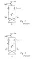
- Figure 1 shows a typical LC oscillator circuit referred to in the art as a tuned oscillator, or a tuned LC oscillator, or a balanced two-phase tuned LC oscillator. It is desirable to implement the circuit shown in Figure 1 in an integrated circuit chip. However, but for the present invention such is not practicable because when an attempt is made to implement a large inductor on an integrated circuit chip, there is typically associated with the large inductor a correspondingly large resistance appearing in series with the inductor. Thus, when the attempt is made to actually implement the LC oscillator circuit shown Figure 1 , what is achieved is actually an RLC oscillator circuit, as is shown in Figure 2 , rather than the desired LC oscillator circuit.
- the unintended resistance, R has the effect of degrading the Q factor which would have been achieved had the unintended resistance not been present (that is, had only the LC components been present). It is essentially the unintended resistance, R, which makes the implementation of such passive LC oscillators circuits impracticable but for embodiments of the present invention.
- the objective is to the achieve an implementation of a typical LC oscillator circuit as shown in Figure 1 in an integrated circuit chip, but without the attendant resistance as is illustrated in Figure 2 . It has been determined that a practicable approximation of the LC oscillator circuit shown in Figure 1 can be achieved by finding a way to achieve relatively high levels of inductance, L, while keeping the resistance, R, relatively low.
- equation 1 makes clear that in order to closely approximate a mathematically ideal oscillator, it is desirable to achieve large inductance, L, and small resistance, R.
- the present invention makes large L or small R possible.
- An embodiment where this has been achieved is set forth below. This embodiment involves producing spiral-like inductors in the single top metal plane, or in two or more planes (that is, if the chip is a multi-layer structure), where like inductors are connected in parallel.
- Figure 3A illustrates a perspective drawing of a spiral inductor 300 implemented in integrated circuit substrate material 302 (e.g., CMOS). Shown is that spiral inductor 300 can be energized by surface line 304 and via 307 in a manner well-known in the art. Also shown in Figure 3A is that the coils forming spiral inductor 300 can be grouped into outer spiral coils 303 and inner spiral coils 305 .
- integrated circuit substrate material 302 e.g., CMOS
- Figure 3B shows a circuit diagram associated with the spiral inductor illustrated in Figure 3A . Shown is that the spiral inductor has resistance R1 306 and inductance L1 308 when driven by current source 309 which produces a current I of a defined magnitude and frequency.
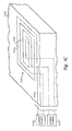
- Figures 4A, 4B, 4C , and 4D illustrate one embodiment of the present invention that produces a new type of spiral inductor which can be utilized to produce Q factor enhancement of LC oscillators.
- the embodiment of Figures 4A, 4B, 4C, and 4D achieves this by making it possible to produce a good spiral inductor with high inductance and very low resistance.
- the technique by which this is done is referred to herein as "replica shielding.” This technique is illustrated in Figures 4A and 4B .
- Figure 4A shows an overhead perspective view of a spiral inductor, modified in accord with the present invention.
- Shown in Figure 4A is a composite spiral inductor 400 implemented in integrated substrate material 302 .
- Composite spiral inductor 400 is composed of an outer spiral coil 402 and an inner spiral coil 404 .
- Outer spiral coil 402 and inner spiral coil 404 are geometrically arranged in the same plane such that they closely approximate outer spiral coils 303 and inner spiral coils 305 of spiral coil inductor 300 , which appears as a one- piece coil in Figure 3A .
- inner coil 404 can be energized by via 410 and via 412 .
- Figure 4B illustrates a circuit diagram associated with composite spiral inductor 400 illustrated in Figure 4A . Shown is that outer spiral coil 402 has resistance R2 414 and inductance L2 416 when driven by a current source operating at some defined magnitude and frequency. Also shown is that inner spiral coil 404 has resistance R3 420 and inductance L3 422 when driven by a current source operating at some defined magnitude and frequency. It has been found that the structure of composite inductor 400 can be used to produce an inductor with relatively high inductance, L, and relatively low resistance, R, which can be utilized to provide an oscillator with high Q factor.
- FIG. 4C Shown in Figure 4C is how outer spiral coil 402 and inner spiral coil 404 can be energized to create an inductor with relatively high inductance, L, and relatively low resistance, R, which can be utilized to provide an oscillator with high Q factor. Shown is that outer spiral coil 402 is driven by electrical current source 428 which produces a current I o and that inner spiral coil 404 is driven by current mirror 430 which produces a current I i .
- Current mirror 430 is an electrical source which mimics electrical current source 428 (it has been found that in a preferred embodiment a crucial factor in such mimicking is to ensure that (1) the direction and phase of I i mimics as nearly as is practicable the direction and phase of current I o and that (2) the magnitude of I i be greater than or equal to the magnitude of I o ). That is, in a preferred embodiment inner spiral coil 404 is driven by current I i at least the same magnitude as and in phase with current I o driving outer spiral coil 402 .
- outer spiral coil 402 and inner spiral coil 404 links to create an effective inductance for outer spiral coil numeral 402 approximately equal to outer spiral coil inductance L o 312 associated with outer spiral coils 303 , and an effective inductance for inner spiral coil 404 approximately equal to inner spiral coil inductance L i 316 associated with inner spiral coils 305 .
- the structure of composite spiral inductor 400 can be used to achieve an oscillator with higher Q than that without such an embodiment of the present invention. Why this is true can be seen by reference to equation 1.
- the Q of an oscillator is directly dependent upon the ratio of L/R (inductance to resistance).
- L/R inductance to resistance
- outer coil 402 as the oscillator coil in the fashion described below in Figures 5A and 5B
- Figure 4D shows a circuit diagram of the circuit shown in Figure 4C .
- outer spiral coil 402 has effective resistance R4 434 approximately equal to resistance outer spiral coils resistance R o 310 and inductance L4 436 approximately equal to outer spiral coils inductance L o 312 .
- inner spiral coil 404 has resistance R5 439 approximately equal to inner spiral coils resistance R i 314 and inductance L5 441 approximately equal to inner spiral coils inductance L i 316 .
- Figure 5A depicts a partially schematic quasi-circuit diagram which shows how the embodiment set forth in Figures 4A-4D can be utilized to provide an improved LC oscillator.
- Shown in Figure 5A is LC oscillator 500 .
- LC oscillator 500 is essentially the oscillator shown in Figure 2 , but with the resistive inductive elements of the oscillator of Figure 2 replaced with the embodiment set forth in Figure 4C .
- outer coil 402 and inner coil 404 are shown in plan view.
- Oscillator current is supplied from source V dd 502 which serves to supply current to outer spiral coils 402 in a fashion analogous to that of current source 428 described earlier, which only directly feeds outer spiral coils 402 .
- a current mirror source (not shown), serves to supply current to inner spiral coils 404 oscillator current sources 428 in a fashion analogous to that of current source 428 described earlier.
- the current mirror source is used to drive inner spiral coils 404 such that the current in each inner spiral coil 404 is of greater than or equal magnitude, in the same direction as, and in phase with the current in its correspondent outer spiral coil 402 .
- the rest of LC oscillator 500 is as was illustrated in Figure 2 .
- a mirror current source such that the currents in an inner coil 404 -outer coil 402 pair are such that the current in inner coil 404 is of greater than or equal magnitude, in the same direction as, and in phase with the current in outer coil 402 .
- One such way is to use a quadrature oscillator and current sources controlled by quadrature phases to produce currents such that currents in each inner and outer coil pair will match in phase, such as that disclosed in pending United States patent application 08/013280, Apparatus and Method for Frequency Tuning a LC Oscillator In a Integrated Circuit.
- Figure 5B illustrates the circuit diagram equivalent to the partially schematic circuit diagram of Figure 5A . Shown is that the resulting circuit diagram is essentially the same as that of the Figure 2 , but with the inductors of the circuit diagram shown Figure 2 replaced with the resulting equivalent circuit shown for outer coil 402 in Figure 4D .
Landscapes
- Engineering & Computer Science (AREA)
- Power Engineering (AREA)
- Manufacturing & Machinery (AREA)
- Microelectronics & Electronic Packaging (AREA)
- Inductance-Capacitance Distribution Constants And Capacitance-Resistance Oscillators (AREA)
- Semiconductor Integrated Circuits (AREA)
Applications Claiming Priority (2)
| Application Number | Priority Date | Filing Date | Title |
|---|---|---|---|
| US09/036,222 US5952893A (en) | 1998-03-06 | 1998-03-06 | Integrated circuit inductors for use with electronic oscillators |
| US36222 | 1998-03-06 |
Publications (2)
| Publication Number | Publication Date |
|---|---|
| EP0940826A2 true EP0940826A2 (de) | 1999-09-08 |
| EP0940826A3 EP0940826A3 (de) | 2000-09-20 |
Family
ID=21887365
Family Applications (1)
| Application Number | Title | Priority Date | Filing Date |
|---|---|---|---|
| EP99300893A Withdrawn EP0940826A3 (de) | 1998-03-06 | 1999-02-08 | Induktor zur Verwendung mit elektronischen Oszillatoren |
Country Status (4)
| Country | Link |
|---|---|
| US (1) | US5952893A (de) |
| EP (1) | EP0940826A3 (de) |
| JP (1) | JP3321109B2 (de) |
| TW (1) | TW414899B (de) |
Cited By (2)
| Publication number | Priority date | Publication date | Assignee | Title |
|---|---|---|---|---|
| FR2812445A1 (fr) * | 2000-07-31 | 2002-02-01 | St Microelectronics Sa | Structure integree d'inductances a valeurs partagees sur un substrat semiconducteur |
| WO2002080349A1 (en) * | 2001-03-30 | 2002-10-10 | Koninklijke Philips Electronics N.V. | Oscillator with improved magnetic coupling rejection |
Families Citing this family (23)
| Publication number | Priority date | Publication date | Assignee | Title |
|---|---|---|---|---|
| EP0969512B1 (de) * | 1998-06-30 | 2009-05-13 | Asulab S.A. | Induktiver Sensor |
| US6201287B1 (en) * | 1998-10-26 | 2001-03-13 | Micron Technology, Inc. | Monolithic inductance-enhancing integrated circuits, complementary metal oxide semiconductor (CMOS) inductance-enhancing integrated circuits, inductor assemblies, and inductance-multiplying methods |
| US6249191B1 (en) | 1998-11-23 | 2001-06-19 | Micron Technology, Inc. | Monolithic integrated circuit oscillators, complementary metal oxide semiconductor (CMOS) voltage-controlled oscillators, integrated circuit oscillators, oscillator-forming methods, and oscillation methods |
| US6274937B1 (en) * | 1999-02-01 | 2001-08-14 | Micron Technology, Inc. | Silicon multi-chip module packaging with integrated passive components and method of making |
| JP2002164441A (ja) * | 2000-11-27 | 2002-06-07 | Matsushita Electric Ind Co Ltd | 高周波スイッチ回路装置 |
| US6549096B2 (en) | 2001-03-19 | 2003-04-15 | International Business Machines Corporation | Switched inductor/varactor tuning circuit having a variable integrated inductor |
| JP2003110358A (ja) * | 2001-09-27 | 2003-04-11 | Matsushita Electric Ind Co Ltd | 発振器 |
| JP2005006153A (ja) * | 2003-06-13 | 2005-01-06 | Nec Electronics Corp | 電圧制御発振器 |
| US7460001B2 (en) * | 2003-09-25 | 2008-12-02 | Qualcomm Incorporated | Variable inductor for integrated circuit and printed circuit board |
| US7005920B2 (en) * | 2003-10-30 | 2006-02-28 | Scintera Network | Programmable passive inductor |
| JP2005236482A (ja) * | 2004-02-18 | 2005-09-02 | Fujitsu Ltd | Lc発振器 |
| US7026880B2 (en) * | 2004-05-13 | 2006-04-11 | Winbond Electronics Corp. | Quadrature VCO using symmetrical spiral inductors and differential varactors |
| US7432794B2 (en) * | 2004-08-16 | 2008-10-07 | Telefonaktiebolaget L M Ericsson (Publ) | Variable integrated inductor |
| JP2006120735A (ja) * | 2004-10-19 | 2006-05-11 | Matsushita Electric Ind Co Ltd | インダクタ装置 |
| JP2006319621A (ja) * | 2005-05-12 | 2006-11-24 | Matsushita Electric Ind Co Ltd | 発振器およびこれを用いたpll回路 |
| FR2913145B1 (fr) * | 2007-02-22 | 2009-05-15 | Stmicroelectronics Crolles Sas | Assemblage de deux parties de circuit electronique integre |
| WO2009082706A1 (en) | 2007-12-21 | 2009-07-02 | The Trustees Of Columbia University In The City Of New York | Active cmos sensor array for electrochemical biomolecular detection |
| US8018312B2 (en) * | 2008-02-12 | 2011-09-13 | International Business Machines Corporation | Inductor and method of operating an inductor by combining primary and secondary coils with coupling structures |
| JP5494214B2 (ja) * | 2010-05-14 | 2014-05-14 | ルネサスエレクトロニクス株式会社 | 半導体装置 |
| WO2013109889A2 (en) * | 2012-01-18 | 2013-07-25 | The Trustees Of Columbia University In The City Of New York | Systems and methods for integrated voltage regulators |
| US10186371B2 (en) * | 2013-07-08 | 2019-01-22 | Samsung Electronics Co., Ltd. | Magnetic field generation apparatus having planar structure |
| RU2552514C2 (ru) * | 2013-07-08 | 2015-06-10 | Корпорация "САМСУНГ ЭЛЕКТРОНИКС Ко., Лтд." | Планарное устройство для генерации магнитного поля с произвольным направлением |
| US9342710B2 (en) * | 2013-11-21 | 2016-05-17 | Nxp B.V. | Electronic tamper detection |
Family Cites Families (9)
| Publication number | Priority date | Publication date | Assignee | Title |
|---|---|---|---|---|
| JPS6265850U (de) * | 1985-10-15 | 1987-04-23 | ||
| JPH0377360A (ja) * | 1989-08-18 | 1991-04-02 | Mitsubishi Electric Corp | 半導体装置 |
| TW275152B (de) * | 1993-11-01 | 1996-05-01 | Ikeda Takeshi | |
| JPH07220927A (ja) * | 1994-02-08 | 1995-08-18 | Murata Mfg Co Ltd | インダクタおよびこれを用いた誘電体共振器 |
| US5497337A (en) * | 1994-10-21 | 1996-03-05 | International Business Machines Corporation | Method for designing high-Q inductors in silicon technology without expensive metalization |
| US5559360A (en) * | 1994-12-19 | 1996-09-24 | Lucent Technologies Inc. | Inductor for high frequency circuits |
| US5656849A (en) * | 1995-09-22 | 1997-08-12 | International Business Machines Corporation | Two-level spiral inductor structure having a high inductance to area ratio |
| US5760456A (en) * | 1995-12-21 | 1998-06-02 | Grzegorek; Andrew Z. | Integrated circuit compatible planar inductors with increased Q |
| JP3712787B2 (ja) * | 1996-05-14 | 2005-11-02 | 新潟精密株式会社 | Fm受信機 |
-
1998
- 1998-03-06 US US09/036,222 patent/US5952893A/en not_active Expired - Fee Related
-
1999
- 1999-02-08 EP EP99300893A patent/EP0940826A3/de not_active Withdrawn
- 1999-02-10 TW TW088102068A patent/TW414899B/zh not_active IP Right Cessation
- 1999-02-24 JP JP04659799A patent/JP3321109B2/ja not_active Expired - Fee Related
Cited By (6)
| Publication number | Priority date | Publication date | Assignee | Title |
|---|---|---|---|---|
| FR2812445A1 (fr) * | 2000-07-31 | 2002-02-01 | St Microelectronics Sa | Structure integree d'inductances a valeurs partagees sur un substrat semiconducteur |
| EP1178500A1 (de) * | 2000-07-31 | 2002-02-06 | STMicroelectronics S.A. | Induktive integrierte Struktur mit geteilten Werten auf einem Halbleitersubstrat |
| US6993313B2 (en) | 2000-07-31 | 2006-01-31 | Stmicroelectronics S.A. | Integrated structure of inductances with shared values on a semiconductor substrate |
| US7751793B2 (en) | 2000-07-31 | 2010-07-06 | Stmicroelectronics S.A. | Integrated structure of inductances with shared values on a semiconductor substrate |
| WO2002080349A1 (en) * | 2001-03-30 | 2002-10-10 | Koninklijke Philips Electronics N.V. | Oscillator with improved magnetic coupling rejection |
| US6512422B2 (en) | 2001-03-30 | 2003-01-28 | Koninklijke Philips Electronics N.V. | Oscillator with improved magnetic coupling rejection |
Also Published As
| Publication number | Publication date |
|---|---|
| US5952893A (en) | 1999-09-14 |
| JP3321109B2 (ja) | 2002-09-03 |
| JPH11330366A (ja) | 1999-11-30 |
| TW414899B (en) | 2000-12-11 |
| EP0940826A3 (de) | 2000-09-20 |
Similar Documents
| Publication | Publication Date | Title |
|---|---|---|
| US5952893A (en) | Integrated circuit inductors for use with electronic oscillators | |
| US5912596A (en) | Apparatus and method for frequency tuning an LC oscillator in a integrated clock circuit | |
| CN101253585B (zh) | 可变集成电感器 | |
| US8102216B1 (en) | Voltage controlled oscillator having reduced phase noise | |
| US7936224B2 (en) | Voltage controlled oscillator | |
| EP3093989B1 (de) | Induktorkondensatorbehälter für resonator | |
| JPH07307619A (ja) | 発振器 | |
| US8072280B2 (en) | Voltage-controlled oscillator | |
| US20160036382A1 (en) | Low power wide tuning range oscillator | |
| US20050156681A1 (en) | Voltage controlled oscillator | |
| US11527992B2 (en) | Rotary traveling wave oscillators with distributed stubs | |
| US10153728B2 (en) | Semiconductor device and method | |
| US20170257082A1 (en) | Circuits and Methods of Synchronizing Differential Ring-Type Oscillators | |
| Decanis et al. | A mm-wave quadrature VCO based on magnetically coupled resonators | |
| US6060759A (en) | Method and apparatus for creating improved inductors for use with electronic oscillators | |
| WO2008069444A1 (en) | Ultra-low power pulse generator for multiband impulse radio-ultra wideband system and method using the same | |
| US10965331B2 (en) | Broad range voltage-controlled oscillator | |
| US9866173B2 (en) | Coupling structure for inductive device | |
| Balodi et al. | Ultra-wideband Quadrature LC-VCO using Capacitor-Bank and backgate topology with on-chip spirally stacked inductor in 0.13 μm RF-CMOS process covering S–C bands | |
| US6188292B1 (en) | Two interconnected oscillators having adjustable coupling for controlling frequency | |
| JP2004056818A (ja) | 発振器、pll回路、通信機器、発振方法 | |
| JPH0763152B2 (ja) | 発振器タンク回路 | |
| EP2434639A1 (de) | LC-Oszillator mit schaltbarem Kondensator-Array | |
| EP3220546A1 (de) | Elektronische treiberschaltung für mindestens einen leistungs-mosfet und verfahren zum betrieb von mindestens einem leistungs-mosfet | |
| US11196382B1 (en) | Oscillator with inductor and programmable capacitor bank |
Legal Events
| Date | Code | Title | Description |
|---|---|---|---|
| PUAI | Public reference made under article 153(3) epc to a published international application that has entered the european phase |
Free format text: ORIGINAL CODE: 0009012 |
|
| AK | Designated contracting states |
Kind code of ref document: A2 Designated state(s): DE FR GB |
|
| AX | Request for extension of the european patent |
Free format text: AL;LT;LV;MK;RO;SI |
|
| PUAL | Search report despatched |
Free format text: ORIGINAL CODE: 0009013 |
|
| AK | Designated contracting states |
Kind code of ref document: A3 Designated state(s): AT BE CH CY DE DK ES FI FR GB GR IE IT LI LU MC NL PT SE |
|
| AX | Request for extension of the european patent |
Free format text: AL;LT;LV;MK;RO;SI |
|
| RIC1 | Information provided on ipc code assigned before grant |
Free format text: 7H 01F 17/00 A, 7H 01F 41/04 B, 7H 01L 27/08 B |
|
| 17P | Request for examination filed |
Effective date: 20010302 |
|
| AKX | Designation fees paid |
Free format text: DE FR GB |
|
| 17Q | First examination report despatched |
Effective date: 20060220 |
|
| STAA | Information on the status of an ep patent application or granted ep patent |
Free format text: STATUS: THE APPLICATION IS DEEMED TO BE WITHDRAWN |
|
| 18D | Application deemed to be withdrawn |
Effective date: 20080402 |