EP0941643B1 - Socle pour circuit integre - Google Patents
Socle pour circuit integre Download PDFInfo
- Publication number
- EP0941643B1 EP0941643B1 EP97951096A EP97951096A EP0941643B1 EP 0941643 B1 EP0941643 B1 EP 0941643B1 EP 97951096 A EP97951096 A EP 97951096A EP 97951096 A EP97951096 A EP 97951096A EP 0941643 B1 EP0941643 B1 EP 0941643B1
- Authority
- EP
- European Patent Office
- Prior art keywords
- base
- circuit board
- printed
- frame
- integrated circuit
- Prior art date
- Legal status (The legal status is an assumption and is not a legal conclusion. Google has not performed a legal analysis and makes no representation as to the accuracy of the status listed.)
- Expired - Lifetime
Links
Images


Classifications
-
- H—ELECTRICITY
- H05—ELECTRIC TECHNIQUES NOT OTHERWISE PROVIDED FOR
- H05K—PRINTED CIRCUITS; CASINGS OR CONSTRUCTIONAL DETAILS OF ELECTRIC APPARATUS; MANUFACTURE OF ASSEMBLAGES OF ELECTRICAL COMPONENTS
- H05K7/00—Constructional details common to different types of electric apparatus
- H05K7/02—Arrangements of circuit components or wiring on supporting structure
- H05K7/10—Plug-in assemblages of components, e.g. IC sockets
- H05K7/1053—Plug-in assemblages of components, e.g. IC sockets having interior leads
- H05K7/1076—Plug-in assemblages of components, e.g. IC sockets having interior leads co-operating by sliding
- H05K7/1084—Plug-in assemblages of components, e.g. IC sockets having interior leads co-operating by sliding pin grid array package carriers
-
- H—ELECTRICITY
- H10—SEMICONDUCTOR DEVICES; ELECTRIC SOLID-STATE DEVICES NOT OTHERWISE PROVIDED FOR
- H10W—GENERIC PACKAGES, INTERCONNECTIONS, CONNECTORS OR OTHER CONSTRUCTIONAL DETAILS OF DEVICES COVERED BY CLASS H10
- H10W78/00—Detachable holders for supporting packaged chips in operation
Definitions
- the invention relates to a base for an integrated Circuit according to the preamble of claim 1.
- a base according to the preamble of claim 1 is known, for example, from US-A-4,679,318.
- Such a base is known from DE-GM 87 16 007, which in addition to cooling the integrated circuit a heat sink that snaps into a carrier frame is equipped.
- Contact elements of the base for contacting the circuit board connector elements are like those the integrated circuit as pins for push-through installation executed. So also for mounting the base Vias in the circuit board required.
- a shielding housing is known from DE 39 22 461 C2 can be used to accommodate various circuits can.
- the housing is essentially cuboid and has an open side on that when it's on a circuit board is mounted, is closed by this. Is attached the shield case on the circuit board by placing four on the lower edge of the shield housing trained mounting legs inserted into assembly openings of the circuit board and bent or be soldered. Housed in the shield case Circuits are soldered directly to the circuit board.
- This shielding case makes an already difficult one Replacement of used components in a disadvantageous way additionally difficult. Another disadvantage is that the Encapsulation of the components has a negative effect on cooling, which is particularly important for complex integrated circuits must be guaranteed.
- the invention has for its object a base for to create an integrated circuit that is easy Exchange of inserted integrated circuits enables and in which on plated-through holes as connection elements the circuit board can be dispensed with.
- the invention has the advantage that also integrated circuits with PGA or SPGA connection forms, which are actually for a push-through assembly are designed on a circuit board Equipped with pure SMD (Surface Mounted Device) technology can be without breaking the SMD principle must become.
- SMD Surface Mounted Device
- socket inserts can be used the one on the integrated circuit side as ZIF (Zero Insertion Force) or LIF (Low Insertion Force) version are executed. So with other base inserts the pulling forces are not on the connection elements of the circuit board act, a removal tool can be used advantageously that is supported on the base, or the base insert can be attached to the circuit board with separate fasteners, e.g. B. screws are held.
- ZIF Zero Insertion Force
- LIF Low Insertion Force
- the lid for removing the integrated circuit can be opened, this has the advantage that the Integrated circuit after opening the housing cover is accessible and from a base insert - possibly under Using a simple removal tool - taken can be.
- the lid can be opened easily for example with screws, clips or a snap connection be attached. Because on the PCB side SMD connection technology is used, it is advantageous to the Base insert with jammed contact elements in its position through the base frame that attaches to the circuit board is to secure. This avoids that during removal pull-out forces occurring on the integrated circuit electrical contact points on the connection elements of the Printed circuit boards work and damage them.
- the base frame serves in an advantageous manner Way as a counter bearing located close to the component with good leverage.
- the design of the Base frame designed so that a special removal tool, which is also used to impress the component can be used.
- One out of several Partly assembled base frames can be beneficial different frame types based on a modular principle being constructed. This does not have a negative effect on the shielding properties of the housing regarding electromagnetic or electrostatic influences if the Overlap parts at the joints.
- For better cooling can cover and frame of the base as provided with cooling fins Heatsinks are formed.
- the lid and the integrated circuit this form-fitting, possibly thermally coupled through a thermal paste, on top of the integrated Circuit on.
- the use is also between cover and frame a thermal paste advantageous.
- the one in cooling active surface can be enlarged further, by placing a bottom plate on the opposite side of the Printed circuit board attached and with frame and cover of the housing is thermally coupled.
- the base plate can also be used as Counter bearing when assembling a base insert for jamming serve the contact elements. With BGA or SGA design of the base insert is the base plate for better cooling and advantageously as a counter bearing, d. H. without one Recess, executed.
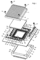
- FIG. 1 there is a base for an integrated circuit 1 essentially from a cover 2, one here four parts 3, 4, 5 and 6 composite frame, one Base insert 7 and a bottom 8.
- the cover 2 is used as a heat sink executed and provided with cooling fins on its top, so that it corresponds to the air flow in the device, in which a printed circuit board equipped with the components shown 9 should be used, optimally aligned can.
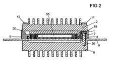
- the lid is attached to the base frame with four screws 10 ... 13 arranged in the area of its corners. For this purpose, in parts 3 ... 6 of the base frame Screws 10 ... 13 corresponding openings with internal thread attached, of which only the openings in Figure 2 14, 15 and 16 are visible.
- the parts 3 ... 6 each have one Collar 17, 18, 19 and 20 on the cover 2 to the assigned Edge sections slightly protruded on the side.
- the base frame can also be made in one piece Frame with fewer attachment points on the PCB can be designed.
- the lid 2 just on top of the integrated circuit 1 on. This already provides good heat coupling reached between integrated circuit 1 and cover 2.
- the top can further improve heat coupling the integrated circuit 1 during assembly with a thermal paste or a similar agent, e.g. B. thermal foil, be provided.
- a thermal paste or a similar agent e.g. B. thermal foil
- the floor 8 can also be executed as a support or Counter bearings are used when a base insert 7 with contact elements is used by pressing the base insert 7 jammed against the circuit board 9 in their guides become. If the heat coupling between floor 8 and Base frame over the eight fastening screws and the Contact points on the printed circuit board 9 are still not sufficient, can like on the top of the edges of the bottom 8 also on the underside of parts 3 ... 6 of the base frame further recesses, not shown in FIG. 1, as a deposit for thermal paste. Because on both sides the circuit board 9 heat sink are provided, the overall height of the base on both sides of the circuit board 9 distributed. So there is only a small one on each side Height above the printed circuit board 9 to implement the Cooling of the integrated circuit 1 is required.
- parts 3 ... 6 of the Base frame obliquely recesses 42, 43, 44 or 45 in which a removal tool, for example a screwdriver blade, can be inserted in such a way that it engages behind the bottom of the integrated circuit 1.
- parts 3 ... 6 may serve as Counter bearing to create leverage.
- Figures 3, 4 and 5 illustrate different variants for clamping a contact element in the base insert after Press on a circuit board 55. It is shown in each case the situation immediately before pressing.
- Contact elements 56, 57 and 58 are each with a contact spring 59 for Contacting the connection element of an integrated to be used Provide circuit.
- a plastic body 60, 61 or 62 the contact elements 56, 57 and 58 from above used and by a snap connection in their end position secured against falling out. Pressed onto the circuit board 55 and the plastic bodies 60 are fastened there, 61 and 62 each with a frame 63, which is directly on the PCB is attachable.
- tolerance compensation dimensions A, B, C and D are shown in FIG.
- the contact elements 56, 57 and 58 are in all three versions of a clamp can be moved in their guides, height tolerances of the connection elements on the circuit board 55 to be able to compensate.
- Dimension B determines the way around which the contact elements 56, 57 and 58 when pressed the base inserts against the circuit board 55 from their end position in the plastic body 60, 61 and 62 are shifted to to generate a clamping effect in the guide.
- a web on frame 63 48 attached, the bottom of which on the top of a Edge of the plastic body 60, 61 and 62 of the base inserts lies on.
- roof-shaped extensions 49 are provided.
- a non-positive clamping of the contact element 56 in the plastic body 60 is achieved by a circumferential collar 64 of the contact element when pressed 56 in a conical bevel 65 of the plastic body 60 pushes in and there by mutual jamming is held.
- a positive clamping results in the variant of Figure 4, in which a first hollow-conical collar 66 on the shaft of the contact element 57 abuts and when pressed against the circuit board 55 through deforms a circumferential collar 67 of the contact element 57 becomes. This makes a positive fit in the plastic part 61 Connection to collar 67 formed.
- the contact element 58 with a circumferential, deformable pointed collar 68, which presses into the plastic part 62 and a positive and non-positive clamping causes.
- FIGs 3, 4 and 5 thus ensures that when pulling out an integrated Circuit 1, which is designed as a PGA or SPGA component may be no forces on the solder joints on the circuit board 55 act.
- Contact elements 53 of the base insert shown in Figure 6 are soldered to connection areas of the circuit board, that are on the surface of the circuit board.
- SMT Surface Mounted Technology
- the base insert is through Centering pins 54, to which the circuit board corresponds Has holes, positioned exactly before the soldering process becomes.
- hermetically sealed Completed "island” is formed, optionally in one Ground concept firmly integrated or also inductive or capacitive can be coupled with a modified Design with enlarged interior of the base or in Free space 55 within the base insert 7 more regarding electromagnetic shielding critical components, e.g. B. Quartz, VCO or clock circuits, in the shield housing integrate. This is particularly favorable for components that are functionally assigned to the integrated circuit.
- electromagnetic shielding critical components e.g. B. Quartz, VCO or clock circuits
- the base can only be replaced the base insert 7 for integrated circuits different Housing designs and different electrical Connection elements are used.
- a base with a Base insert and a shielded housing described.
- a base in another embodiment of the invention also only consist of a base insert with the contact elements.
Landscapes
- Engineering & Computer Science (AREA)
- Microelectronics & Electronic Packaging (AREA)
- Shielding Devices Or Components To Electric Or Magnetic Fields (AREA)
- Coupling Device And Connection With Printed Circuit (AREA)
- Details Of Connecting Devices For Male And Female Coupling (AREA)
Claims (18)
- Socle pour un circuit intégré, qui convient au montage sur une plaquette (9) à circuit imprimé et qui est muni d'un insert (7) de socle à éléments (53) de contact par lesquels des liaisons électriques entre des pins du circuit (1) intégré, réalisées pour un montage par enfichage dans une plaquette à circuit imprimé, et des éléments de raccordement de la plaquette (9) à circuit imprimé peuvent être produits, les éléments (53) de contact étant réalisés en une technique de montage en surface pour la mise en contact des éléments de raccordement sur la plaquette (9) à circuit imprimé et pouvant coulisser dans l'insert (7) de socle lors du montage pour la compensation de tolérances de hauteur des éléments de raccordement sur la plaquette (9) à circuit imprimé, caractérisé en ce que le guidage des éléments (53) de contact dans l'insert (7) de socle est réalisé de telle manière qu'ils sont empêchés de coulisser par un blocage des éléments (53) de contact dans l'insert (7) de socle après que l'insert de socle a été repoussé sur la plaquette (9) à circuit imprimé.
- Socle suivant la revendication 1, caractérisé en ce que les éléments (53) de contact sont montés en rangées dans l'insert (7) de socle d'une manière correspondant à une disposition de pins dans le circuit (1) intégré suivant le genre d'un PGA (Pin Grid Array) ou SPGA (Staggered Pin Grid Array).
- Culot suivant la revendication 1 ou 2, caractérisé en ce que les éléments (53) de contact pour la mise en contact des éléments de raccordement sur la plaquette (9) à circuit imprimé sont réalisés en BGA (Ball Grid Array) ou SGA (Stud Grid Array).
- Socle suivant l'une des revendications précédentes, caractérisé en ce que le socle comporte un boítier de blindage ouvert d'un côté en direction de la plaquette (9) à circuit imprimé et comportant un cadre (3 ... 6) et un couvercle (2) pour la réception du circuit (1) imprimé et de l'insert (7) de socle, le couvercle (2) pouvant être ouvert pour retirer le circuit (1) intégré.
- Socle suivant la revendication 4, caractérisé en ce que le cadre (3 ... 6) de socle peut être fixé sur la plaquette (9) à circuit imprimé et, lorsqu'il est monté, bloque l'insert (7) de socle en sa position.
- Socle suivant la revendication 5, caractérisé en ce qu'il est prévu des vis (28 ... 31) pour la fixation du cadre de socle à la plaquette à circuit imprimé.
- Socle suivant la revendication 5 ou 6, caractérisé en ce que le cadre de socle est muni pour le blocage en position de l'insert de socle, sur sa face intérieure, d'une barrette (48) sensiblement circulaire à la face inférieure de laquelle s'applique, à l'état monté, la face supérieure d'une arête (46, 47) circulaire correspondante de l'insert (7) de socle.
- Socle suivant l'une des revendications 4 à 7, caractérisé en ce que le cadre de socle est muni sur sa face intérieure d'au moins un évidement (42 ... 45), notamment d'un biseau, qui permet un accès pour un outil de soulèvement, notamment pour un tournevis, pour soulever le circuit (1 ) intégré.
- Socle suivant l'une des revendications 4 à 8, caractérisé en ce que le cadre de socle est constitué d'un parallélogramme composé de plusieurs parties (3 ... 6) s'étendant chacune sensiblement le long des arêtes rectilignes, les parties se chevauchant les unes les autres au point de jointure qui se trouvent dans la zone des coins du cadre.
- Socle suivant l'une des revendications 4 à 9, caractérisé en ce que le couvercle (2) est réalisé en élément refroidissant, muni de nervures de refroidissement, pour le circuit intégré.
- Socle suivant la revendication 10, caractérisé en ce que le cadre de socle est réalisé en élément refroidissant, muni de nervures de refroidissement.
- Socle suivant la revendication 10 ou 11, caractérisé en ce que le cadre de socle comporte sur les surfaces de support du couvercle des cavités (21 ... 27) pour de la pâte thermoconductrice en vue du couplage thermique du cadre et du couvercle.
- Socle suivant l'une des revendications 4 à 12, caractérisé en ce que le cadre de socle et le couvercle se chevauchent l'un l'autre aux points de jointure.
- Socle suivant l'une des revendications 4 à 13, caractérisé en ce qu'il est prévu une plaque (8) de fond pour le montage sur la face de la plaquette (9) à circuit imprimé qui fait face au cadre et au couvercle.
- Socle suivant la revendication 14, caractérisé en ce que la plaque (8) de fond est réalisée en élément refroidissant, muni de nervures de refroidissement, et, à l'état monté, est couplée thermiquement avec le circuit intégré par des évidements (32, 33, 34) de la plaquette à circuit imprimé, par l'intermédiaire du cadre de socle et/ou du couvercle de socle.
- Socle suivant la revendication 14 ou 15, caractérisé en ce qu'il peut être fixé par blocage de la plaquette à circuit imprimé entre le cadre de socle et la plaque de fond.
- Socle suivant la revendication 16, caractérisé en ce que le cadre de socle et la plaque de fond peuvent être vissés ensemble par les vis (28 ... 31) faisant saillie de la plaquette à circuit imprimé.
- Socle suivant l'une des revendications 14 à 17, caractérisé en ce que la plaque de fond comporte un évidement (41) pour des éléments de raccordement ou des composants faisant saillie par la plaquette à circuit imprimé sur la face inférieure de la plaquette (9) à circuit imprimé.
Applications Claiming Priority (3)
| Application Number | Priority Date | Filing Date | Title |
|---|---|---|---|
| DE29620593U DE29620593U1 (de) | 1996-11-26 | 1996-11-26 | Sockel für eine integrierte Schaltung |
| DE29620593U | 1996-11-26 | ||
| PCT/DE1997/002758 WO1998024284A1 (fr) | 1996-11-26 | 1997-11-25 | Socle pour circuit integre |
Publications (2)
| Publication Number | Publication Date |
|---|---|
| EP0941643A1 EP0941643A1 (fr) | 1999-09-15 |
| EP0941643B1 true EP0941643B1 (fr) | 2000-09-06 |
Family
ID=8032495
Family Applications (1)
| Application Number | Title | Priority Date | Filing Date |
|---|---|---|---|
| EP97951096A Expired - Lifetime EP0941643B1 (fr) | 1996-11-26 | 1997-11-25 | Socle pour circuit integre |
Country Status (5)
| Country | Link |
|---|---|
| EP (1) | EP0941643B1 (fr) |
| AT (1) | ATE196222T1 (fr) |
| DE (2) | DE29620593U1 (fr) |
| ES (1) | ES2152709T3 (fr) |
| WO (1) | WO1998024284A1 (fr) |
Families Citing this family (2)
| Publication number | Priority date | Publication date | Assignee | Title |
|---|---|---|---|---|
| JP3161423B2 (ja) * | 1998-08-11 | 2001-04-25 | 日本電気株式会社 | Lsiの実装構造 |
| DE20117526U1 (de) * | 2001-10-26 | 2003-03-06 | EKL AG, 88299 Leutkirch | Elektromagnetische Abschirmung für Mikroprozessoren |
Citations (1)
| Publication number | Priority date | Publication date | Assignee | Title |
|---|---|---|---|---|
| US4679318A (en) * | 1986-02-06 | 1987-07-14 | Amp Incorporated | Application tool and method for positioning electrical sockets on circuit boards for surface soldering |
Family Cites Families (19)
| Publication number | Priority date | Publication date | Assignee | Title |
|---|---|---|---|---|
| DE2919058A1 (de) * | 1979-05-10 | 1980-11-20 | Siemens Ag | Elektronisches geraet mit mindestens einer leiterplatte |
| DE3439556A1 (de) * | 1984-08-07 | 1986-02-20 | Aavid Engineering Inc., Laconia, N.H. | Eine waermesenke bildende abdeckung fuer einen ein elektronisches chip aufnehmenden traeger |
| DE3629567A1 (de) * | 1986-08-30 | 1988-03-03 | Bbc Brown Boveri & Cie | Halbleiterblock |
| DE8716007U1 (de) * | 1987-12-03 | 1989-01-05 | Siemens AG, 1000 Berlin und 8000 München | Vorrichtung zur Abführung von Verlustwärme aus integrierten Schaltungen |
| JPH062316Y2 (ja) * | 1988-07-08 | 1994-01-19 | アルプス電気株式会社 | シールドケースの底面カバー取付構造 |
| DE3910518A1 (de) * | 1989-04-01 | 1990-10-04 | Manfred Haller | Schaltungsplatine fuer die optimale entkopplung von schaltungen mit digitalen ic's |
| US4969828A (en) * | 1989-05-17 | 1990-11-13 | Amp Incorporated | Electrical socket for TAB IC's |
| US5151039A (en) * | 1990-04-06 | 1992-09-29 | Advanced Interconnections Corporation | Integrated circuit adapter having gullwing-shaped leads |
| US5058265A (en) * | 1990-05-10 | 1991-10-22 | Rockwell International Corporation | Method for packaging a board of electronic components |
| US5303466A (en) * | 1991-03-25 | 1994-04-19 | Daiichi Denshi Kogyo Kabushiki Kaisha | Method of mounting surface connector |
| DE4326207A1 (de) * | 1992-10-06 | 1994-04-07 | Hewlett Packard Co | Mechanisch schwimmendes Mehr-Chip-Substrat |
| JPH06164265A (ja) * | 1992-11-16 | 1994-06-10 | Toshiba Corp | マイクロ波増幅器 |
| US5302853A (en) * | 1993-01-25 | 1994-04-12 | The Whitaker Corporation | Land grid array package |
| DE4310446C1 (de) * | 1993-03-31 | 1994-05-05 | Export Contor Ausenhandelsgese | Schaltungsanordnung |
| US5396403A (en) * | 1993-07-06 | 1995-03-07 | Hewlett-Packard Company | Heat sink assembly with thermally-conductive plate for a plurality of integrated circuits on a substrate |
| US5473510A (en) * | 1994-03-25 | 1995-12-05 | Convex Computer Corporation | Land grid array package/circuit board assemblies and methods for constructing the same |
| DE19511229A1 (de) * | 1994-03-28 | 1995-10-05 | Whitaker Corp | Chipträgersystem |
| DE4420527A1 (de) * | 1994-06-13 | 1995-06-29 | Siemens Nixdorf Inf Syst | Verbindungssystem zum Kontaktieren von Bauelementen mit Pinanschluß und Finepitch-Rasterung auf Leiterplatten |
| GB2293502A (en) * | 1994-09-26 | 1996-03-27 | Methode Electronics Inc | Miniature grid array socketing system |
-
1996
- 1996-11-26 DE DE29620593U patent/DE29620593U1/de not_active Expired - Lifetime
-
1997
- 1997-11-25 ES ES97951096T patent/ES2152709T3/es not_active Expired - Lifetime
- 1997-11-25 WO PCT/DE1997/002758 patent/WO1998024284A1/fr not_active Ceased
- 1997-11-25 DE DE59702325T patent/DE59702325D1/de not_active Expired - Fee Related
- 1997-11-25 EP EP97951096A patent/EP0941643B1/fr not_active Expired - Lifetime
- 1997-11-25 AT AT97951096T patent/ATE196222T1/de not_active IP Right Cessation
Patent Citations (1)
| Publication number | Priority date | Publication date | Assignee | Title |
|---|---|---|---|---|
| US4679318A (en) * | 1986-02-06 | 1987-07-14 | Amp Incorporated | Application tool and method for positioning electrical sockets on circuit boards for surface soldering |
Also Published As
| Publication number | Publication date |
|---|---|
| DE59702325D1 (de) | 2000-10-12 |
| DE29620593U1 (de) | 1998-01-02 |
| WO1998024284A1 (fr) | 1998-06-04 |
| ES2152709T3 (es) | 2001-02-01 |
| EP0941643A1 (fr) | 1999-09-15 |
| ATE196222T1 (de) | 2000-09-15 |
Similar Documents
| Publication | Publication Date | Title |
|---|---|---|
| EP0941642B1 (fr) | Support pour circuit integre | |
| DE69106615T2 (de) | Lageweise zusammengebaute Steckbuchsenleiste mit integraler Erdabschirmung. | |
| DE102007001407B4 (de) | Montageanordnung zur Fixierung übereinander angeordneter Leiterplatten in einem Gehäuse | |
| DE3936906A1 (de) | Gehaeuse fuer kfz-elektronik | |
| DE4321331A1 (de) | Anbausteuergerät | |
| EP3482611B1 (fr) | Système et procédé de connexion à la masse d'une carte de circuit imprimé sur un boîtier d'un appareil électrique | |
| DE3627372C2 (fr) | ||
| EP1282345B1 (fr) | Boîtier abritant une carte électronique avec ses composants dans un véhicule | |
| WO1994014306A1 (fr) | Dispositif a support plastique permettant de loger et de maintenir un module electronique | |
| EP0613331B1 (fr) | Méthode d'attachement d'un circuit hybride sur un circuit imprimé | |
| DE3731413C2 (fr) | ||
| EP0941643B1 (fr) | Socle pour circuit integre | |
| DE19543260C2 (de) | Elektrische Bauelementeanordnung mit mehreren in einem Gehäuse angeordneten elektrischen Bauelementen | |
| DE10123198A1 (de) | Anordnung aus einem Gehäuse und einem Schaltungsträger | |
| DE102007048159B4 (de) | Gehäuse zur Aufnahme elektrischer oder elektronischer Bauteile und/oder Komponenten, inbesondere Hochfrequenzkomponenten | |
| EP1185998B1 (fr) | Dispositif de fixation en position correcte d'une plaquette de circuits imprimes | |
| WO1998024124A1 (fr) | Support pour circuit integre | |
| DE4231140A1 (de) | Baugruppe für elektronische Steuergeräte | |
| EP1010583B1 (fr) | Dispositif électronique | |
| EP2412214B1 (fr) | Cadre de logement pour au moins une carte de circuit imprimé | |
| DE102005038513A1 (de) | Modularisierte Schaltungskomponente | |
| DE19931908C2 (de) | Elektronische Anlage | |
| EP1079476A2 (fr) | Méthode de montage d'un élément électrique sur un circuit imprimé | |
| DE9408831U1 (de) | Aufbausystem für quaderförmige Gehäuse | |
| DE19630503A1 (de) | Vorrichtung zum elektrischen Anschluß eines Gerätes, insbesondere eines Autoradios, in einem Kraftfahrzeug |
Legal Events
| Date | Code | Title | Description |
|---|---|---|---|
| PUAI | Public reference made under article 153(3) epc to a published international application that has entered the european phase |
Free format text: ORIGINAL CODE: 0009012 |
|
| 17P | Request for examination filed |
Effective date: 19990520 |
|
| AK | Designated contracting states |
Kind code of ref document: A1 Designated state(s): AT CH DE ES FR GB LI |
|
| GRAG | Despatch of communication of intention to grant |
Free format text: ORIGINAL CODE: EPIDOS AGRA |
|
| GRAG | Despatch of communication of intention to grant |
Free format text: ORIGINAL CODE: EPIDOS AGRA |
|
| GRAH | Despatch of communication of intention to grant a patent |
Free format text: ORIGINAL CODE: EPIDOS IGRA |
|
| 17Q | First examination report despatched |
Effective date: 19991119 |
|
| GRAH | Despatch of communication of intention to grant a patent |
Free format text: ORIGINAL CODE: EPIDOS IGRA |
|
| GRAA | (expected) grant |
Free format text: ORIGINAL CODE: 0009210 |
|
| AK | Designated contracting states |
Kind code of ref document: B1 Designated state(s): AT CH DE ES FR GB LI |
|
| REF | Corresponds to: |
Ref document number: 196222 Country of ref document: AT Date of ref document: 20000915 Kind code of ref document: T |
|
| REG | Reference to a national code |
Ref country code: CH Ref legal event code: EP |
|
| REF | Corresponds to: |
Ref document number: 59702325 Country of ref document: DE Date of ref document: 20001012 |
|
| REG | Reference to a national code |
Ref country code: CH Ref legal event code: NV Representative=s name: SIEMENS SCHWEIZ AG |
|
| GBT | Gb: translation of ep patent filed (gb section 77(6)(a)/1977) |
Effective date: 20001107 |
|
| ET | Fr: translation filed | ||
| REG | Reference to a national code |
Ref country code: ES Ref legal event code: FG2A Ref document number: 2152709 Country of ref document: ES Kind code of ref document: T3 |
|
| PLBE | No opposition filed within time limit |
Free format text: ORIGINAL CODE: 0009261 |
|
| STAA | Information on the status of an ep patent application or granted ep patent |
Free format text: STATUS: NO OPPOSITION FILED WITHIN TIME LIMIT |
|
| 26N | No opposition filed | ||
| REG | Reference to a national code |
Ref country code: GB Ref legal event code: IF02 |
|
| PGFP | Annual fee paid to national office [announced via postgrant information from national office to epo] |
Ref country code: ES Payment date: 20081216 Year of fee payment: 12 Ref country code: AT Payment date: 20081017 Year of fee payment: 12 |
|
| REG | Reference to a national code |
Ref country code: CH Ref legal event code: PCAR Free format text: SIEMENS SCHWEIZ AG;INTELLECTUAL PROPERTY FREILAGERSTRASSE 40;8047 ZUERICH (CH) |
|
| PGFP | Annual fee paid to national office [announced via postgrant information from national office to epo] |
Ref country code: FR Payment date: 20081118 Year of fee payment: 12 |
|
| PGFP | Annual fee paid to national office [announced via postgrant information from national office to epo] |
Ref country code: DE Payment date: 20090119 Year of fee payment: 12 |
|
| PGFP | Annual fee paid to national office [announced via postgrant information from national office to epo] |
Ref country code: GB Payment date: 20081110 Year of fee payment: 12 Ref country code: CH Payment date: 20090205 Year of fee payment: 12 |
|
| REG | Reference to a national code |
Ref country code: CH Ref legal event code: PL |
|
| GBPC | Gb: european patent ceased through non-payment of renewal fee |
Effective date: 20091125 |
|
| REG | Reference to a national code |
Ref country code: FR Ref legal event code: ST Effective date: 20100730 |
|
| PG25 | Lapsed in a contracting state [announced via postgrant information from national office to epo] |
Ref country code: AT Free format text: LAPSE BECAUSE OF NON-PAYMENT OF DUE FEES Effective date: 20091125 |
|
| PG25 | Lapsed in a contracting state [announced via postgrant information from national office to epo] |
Ref country code: LI Free format text: LAPSE BECAUSE OF NON-PAYMENT OF DUE FEES Effective date: 20091130 Ref country code: FR Free format text: LAPSE BECAUSE OF NON-PAYMENT OF DUE FEES Effective date: 20091130 Ref country code: CH Free format text: LAPSE BECAUSE OF NON-PAYMENT OF DUE FEES Effective date: 20091130 |
|
| PG25 | Lapsed in a contracting state [announced via postgrant information from national office to epo] |
Ref country code: DE Free format text: LAPSE BECAUSE OF NON-PAYMENT OF DUE FEES Effective date: 20100601 |
|
| PG25 | Lapsed in a contracting state [announced via postgrant information from national office to epo] |
Ref country code: GB Free format text: LAPSE BECAUSE OF NON-PAYMENT OF DUE FEES Effective date: 20091125 |
|
| REG | Reference to a national code |
Ref country code: ES Ref legal event code: FD2A Effective date: 20110408 |
|
| PG25 | Lapsed in a contracting state [announced via postgrant information from national office to epo] |
Ref country code: ES Free format text: LAPSE BECAUSE OF NON-PAYMENT OF DUE FEES Effective date: 20110328 |
|
| PG25 | Lapsed in a contracting state [announced via postgrant information from national office to epo] |
Ref country code: ES Free format text: LAPSE BECAUSE OF NON-PAYMENT OF DUE FEES Effective date: 20091126 |