EP0943954A2 - Optische Sicherung - Google Patents
Optische Sicherung Download PDFInfo
- Publication number
- EP0943954A2 EP0943954A2 EP99302152A EP99302152A EP0943954A2 EP 0943954 A2 EP0943954 A2 EP 0943954A2 EP 99302152 A EP99302152 A EP 99302152A EP 99302152 A EP99302152 A EP 99302152A EP 0943954 A2 EP0943954 A2 EP 0943954A2
- Authority
- EP
- European Patent Office
- Prior art keywords
- light
- optical fuse
- optical
- constituent
- heatable
- Prior art date
- Legal status (The legal status is an assumption and is not a legal conclusion. Google has not performed a legal analysis and makes no representation as to the accuracy of the status listed.)
- Withdrawn
Links
- 230000003287 optical effect Effects 0.000 title claims abstract description 242
- 238000002310 reflectometry Methods 0.000 claims abstract description 37
- 239000000470 constituent Substances 0.000 claims description 31
- 230000008859 change Effects 0.000 claims description 14
- 229910052751 metal Inorganic materials 0.000 claims description 14
- 239000002184 metal Substances 0.000 claims description 14
- 239000004065 semiconductor Substances 0.000 claims description 11
- 150000002736 metal compounds Chemical class 0.000 claims description 8
- 238000000151 deposition Methods 0.000 claims description 5
- 239000003989 dielectric material Substances 0.000 claims description 4
- 239000011521 glass Substances 0.000 claims description 4
- 125000000962 organic group Chemical group 0.000 claims description 4
- 239000002245 particle Substances 0.000 claims description 4
- 239000000758 substrate Substances 0.000 claims description 3
- 238000000354 decomposition reaction Methods 0.000 claims 1
- 230000000593 degrading effect Effects 0.000 claims 1
- 239000000463 material Substances 0.000 abstract description 45
- 239000013307 optical fiber Substances 0.000 description 50
- 229910052761 rare earth metal Inorganic materials 0.000 description 21
- 238000000034 method Methods 0.000 description 20
- 239000010410 layer Substances 0.000 description 18
- 230000005540 biological transmission Effects 0.000 description 12
- IEQIEDJGQAUEQZ-UHFFFAOYSA-N phthalocyanine Chemical compound N1C(N=C2C3=CC=CC=C3C(N=C3C4=CC=CC=C4C(=N4)N3)=N2)=C(C=CC=C2)C2=C1N=C1C2=CC=CC=C2C4=N1 IEQIEDJGQAUEQZ-UHFFFAOYSA-N 0.000 description 9
- 230000008569 process Effects 0.000 description 8
- 230000004044 response Effects 0.000 description 8
- VYPSYNLAJGMNEJ-UHFFFAOYSA-N Silicium dioxide Chemical compound O=[Si]=O VYPSYNLAJGMNEJ-UHFFFAOYSA-N 0.000 description 7
- 238000010586 diagram Methods 0.000 description 7
- 239000004372 Polyvinyl alcohol Substances 0.000 description 6
- GWEVSGVZZGPLCZ-UHFFFAOYSA-N Titan oxide Chemical compound O=[Ti]=O GWEVSGVZZGPLCZ-UHFFFAOYSA-N 0.000 description 6
- 239000000835 fiber Substances 0.000 description 6
- 229920002451 polyvinyl alcohol Polymers 0.000 description 6
- KDLHZDBZIXYQEI-UHFFFAOYSA-N Palladium Chemical compound [Pd] KDLHZDBZIXYQEI-UHFFFAOYSA-N 0.000 description 5
- PXHVJJICTQNCMI-UHFFFAOYSA-N Nickel Chemical compound [Ni] PXHVJJICTQNCMI-UHFFFAOYSA-N 0.000 description 4
- 150000001875 compounds Chemical class 0.000 description 4
- 230000006378 damage Effects 0.000 description 4
- 230000008020 evaporation Effects 0.000 description 4
- 238000001704 evaporation Methods 0.000 description 4
- 230000005284 excitation Effects 0.000 description 4
- 238000005259 measurement Methods 0.000 description 4
- BASFCYQUMIYNBI-UHFFFAOYSA-N platinum Chemical compound [Pt] BASFCYQUMIYNBI-UHFFFAOYSA-N 0.000 description 4
- 238000010521 absorption reaction Methods 0.000 description 3
- 238000006243 chemical reaction Methods 0.000 description 3
- 229910052681 coesite Inorganic materials 0.000 description 3
- 238000004891 communication Methods 0.000 description 3
- 239000010949 copper Substances 0.000 description 3
- 229910052906 cristobalite Inorganic materials 0.000 description 3
- 229910052732 germanium Inorganic materials 0.000 description 3
- 230000031700 light absorption Effects 0.000 description 3
- 230000009021 linear effect Effects 0.000 description 3
- 239000011572 manganese Substances 0.000 description 3
- 238000012544 monitoring process Methods 0.000 description 3
- 239000000377 silicon dioxide Substances 0.000 description 3
- 229910052682 stishovite Inorganic materials 0.000 description 3
- 239000010936 titanium Substances 0.000 description 3
- 230000007704 transition Effects 0.000 description 3
- 229910052905 tridymite Inorganic materials 0.000 description 3
- 230000009471 action Effects 0.000 description 2
- 229910052782 aluminium Inorganic materials 0.000 description 2
- 230000008021 deposition Effects 0.000 description 2
- 238000009792 diffusion process Methods 0.000 description 2
- 238000009826 distribution Methods 0.000 description 2
- 239000003822 epoxy resin Substances 0.000 description 2
- 239000002223 garnet Substances 0.000 description 2
- 238000003780 insertion Methods 0.000 description 2
- 230000037431 insertion Effects 0.000 description 2
- -1 lutetium aluminum Chemical compound 0.000 description 2
- 230000009022 nonlinear effect Effects 0.000 description 2
- 239000011368 organic material Substances 0.000 description 2
- 229910052763 palladium Inorganic materials 0.000 description 2
- 229920000647 polyepoxide Polymers 0.000 description 2
- 229940068984 polyvinyl alcohol Drugs 0.000 description 2
- 235000019422 polyvinyl alcohol Nutrition 0.000 description 2
- 229920000915 polyvinyl chloride Polymers 0.000 description 2
- 230000002441 reversible effect Effects 0.000 description 2
- 239000002356 single layer Substances 0.000 description 2
- RYGMFSIKBFXOCR-UHFFFAOYSA-N Copper Chemical compound [Cu] RYGMFSIKBFXOCR-UHFFFAOYSA-N 0.000 description 1
- PXGOKWXKJXAPGV-UHFFFAOYSA-N Fluorine Chemical compound FF PXGOKWXKJXAPGV-UHFFFAOYSA-N 0.000 description 1
- GYHNNYVSQQEPJS-UHFFFAOYSA-N Gallium Chemical compound [Ga] GYHNNYVSQQEPJS-UHFFFAOYSA-N 0.000 description 1
- PWHULOQIROXLJO-UHFFFAOYSA-N Manganese Chemical compound [Mn] PWHULOQIROXLJO-UHFFFAOYSA-N 0.000 description 1
- ZOKXTWBITQBERF-UHFFFAOYSA-N Molybdenum Chemical compound [Mo] ZOKXTWBITQBERF-UHFFFAOYSA-N 0.000 description 1
- XUIMIQQOPSSXEZ-UHFFFAOYSA-N Silicon Chemical compound [Si] XUIMIQQOPSSXEZ-UHFFFAOYSA-N 0.000 description 1
- NINIDFKCEFEMDL-UHFFFAOYSA-N Sulfur Chemical compound [S] NINIDFKCEFEMDL-UHFFFAOYSA-N 0.000 description 1
- RTAQQCXQSZGOHL-UHFFFAOYSA-N Titanium Chemical compound [Ti] RTAQQCXQSZGOHL-UHFFFAOYSA-N 0.000 description 1
- XAGFODPZIPBFFR-UHFFFAOYSA-N aluminium Chemical compound [Al] XAGFODPZIPBFFR-UHFFFAOYSA-N 0.000 description 1
- 229910021486 amorphous silicon dioxide Inorganic materials 0.000 description 1
- 230000003321 amplification Effects 0.000 description 1
- WUKWITHWXAAZEY-UHFFFAOYSA-L calcium difluoride Chemical compound [F-].[F-].[Ca+2] WUKWITHWXAAZEY-UHFFFAOYSA-L 0.000 description 1
- 230000005466 cherenkov radiation Effects 0.000 description 1
- 238000000576 coating method Methods 0.000 description 1
- 229910017052 cobalt Inorganic materials 0.000 description 1
- 239000010941 cobalt Substances 0.000 description 1
- GUTLYIVDDKVIGB-UHFFFAOYSA-N cobalt atom Chemical compound [Co] GUTLYIVDDKVIGB-UHFFFAOYSA-N 0.000 description 1
- 230000000052 comparative effect Effects 0.000 description 1
- 229920001577 copolymer Polymers 0.000 description 1
- 229910052802 copper Inorganic materials 0.000 description 1
- 230000003247 decreasing effect Effects 0.000 description 1
- 238000005137 deposition process Methods 0.000 description 1
- 238000013461 design Methods 0.000 description 1
- 230000000694 effects Effects 0.000 description 1
- 238000005516 engineering process Methods 0.000 description 1
- 238000002474 experimental method Methods 0.000 description 1
- 239000011737 fluorine Substances 0.000 description 1
- 229910052731 fluorine Inorganic materials 0.000 description 1
- 239000010436 fluorite Substances 0.000 description 1
- 229910052733 gallium Inorganic materials 0.000 description 1
- GNPVGFCGXDBREM-UHFFFAOYSA-N germanium atom Chemical compound [Ge] GNPVGFCGXDBREM-UHFFFAOYSA-N 0.000 description 1
- 229910052738 indium Inorganic materials 0.000 description 1
- APFVFJFRJDLVQX-UHFFFAOYSA-N indium atom Chemical compound [In] APFVFJFRJDLVQX-UHFFFAOYSA-N 0.000 description 1
- 150000002500 ions Chemical class 0.000 description 1
- 238000003475 lamination Methods 0.000 description 1
- 229910001635 magnesium fluoride Inorganic materials 0.000 description 1
- 229910052748 manganese Inorganic materials 0.000 description 1
- 238000004519 manufacturing process Methods 0.000 description 1
- 239000011159 matrix material Substances 0.000 description 1
- 239000000203 mixture Substances 0.000 description 1
- 238000012986 modification Methods 0.000 description 1
- 230000004048 modification Effects 0.000 description 1
- 229910052750 molybdenum Inorganic materials 0.000 description 1
- 239000011733 molybdenum Substances 0.000 description 1
- 229910052759 nickel Inorganic materials 0.000 description 1
- 238000003199 nucleic acid amplification method Methods 0.000 description 1
- 150000002902 organometallic compounds Chemical class 0.000 description 1
- 229910052697 platinum Inorganic materials 0.000 description 1
- 238000012545 processing Methods 0.000 description 1
- 238000005086 pumping Methods 0.000 description 1
- 239000010453 quartz Substances 0.000 description 1
- 229910052710 silicon Inorganic materials 0.000 description 1
- 239000010703 silicon Substances 0.000 description 1
- 239000006104 solid solution Substances 0.000 description 1
- 238000007711 solidification Methods 0.000 description 1
- 230000008023 solidification Effects 0.000 description 1
- 239000000243 solution Substances 0.000 description 1
- 238000004544 sputter deposition Methods 0.000 description 1
- 229910052717 sulfur Inorganic materials 0.000 description 1
- 239000011593 sulfur Substances 0.000 description 1
- 229910052719 titanium Inorganic materials 0.000 description 1
- 239000012780 transparent material Substances 0.000 description 1
- 238000001771 vacuum deposition Methods 0.000 description 1
- LEONUFNNVUYDNQ-UHFFFAOYSA-N vanadium atom Chemical compound [V] LEONUFNNVUYDNQ-UHFFFAOYSA-N 0.000 description 1
Images


Classifications
-
- G—PHYSICS
- G02—OPTICS
- G02F—OPTICAL DEVICES OR ARRANGEMENTS FOR THE CONTROL OF LIGHT BY MODIFICATION OF THE OPTICAL PROPERTIES OF THE MEDIA OF THE ELEMENTS INVOLVED THEREIN; NON-LINEAR OPTICS; FREQUENCY-CHANGING OF LIGHT; OPTICAL LOGIC ELEMENTS; OPTICAL ANALOGUE/DIGITAL CONVERTERS
- G02F1/00—Devices or arrangements for the control of the intensity, colour, phase, polarisation or direction of light arriving from an independent light source, e.g. switching, gating or modulating; Non-linear optics
- G02F1/35—Non-linear optics
- G02F1/3525—Optical damage
-
- G—PHYSICS
- G02—OPTICS
- G02B—OPTICAL ELEMENTS, SYSTEMS OR APPARATUS
- G02B6/00—Light guides; Structural details of arrangements comprising light guides and other optical elements, e.g. couplings
- G02B6/24—Coupling light guides
- G02B6/26—Optical coupling means
- G02B6/264—Optical coupling means with optical elements between opposed fibre ends which perform a function other than beam splitting
-
- G—PHYSICS
- G02—OPTICS
- G02F—OPTICAL DEVICES OR ARRANGEMENTS FOR THE CONTROL OF LIGHT BY MODIFICATION OF THE OPTICAL PROPERTIES OF THE MEDIA OF THE ELEMENTS INVOLVED THEREIN; NON-LINEAR OPTICS; FREQUENCY-CHANGING OF LIGHT; OPTICAL LOGIC ELEMENTS; OPTICAL ANALOGUE/DIGITAL CONVERTERS
- G02F1/00—Devices or arrangements for the control of the intensity, colour, phase, polarisation or direction of light arriving from an independent light source, e.g. switching, gating or modulating; Non-linear optics
- G02F1/35—Non-linear optics
-
- G—PHYSICS
- G02—OPTICS
- G02B—OPTICAL ELEMENTS, SYSTEMS OR APPARATUS
- G02B6/00—Light guides; Structural details of arrangements comprising light guides and other optical elements, e.g. couplings
- G02B6/24—Coupling light guides
- G02B6/36—Mechanical coupling means
- G02B6/38—Mechanical coupling means having fibre to fibre mating means
- G02B6/3807—Dismountable connectors, i.e. comprising plugs
- G02B6/3833—Details of mounting fibres in ferrules; Assembly methods; Manufacture
- G02B6/3845—Details of mounting fibres in ferrules; Assembly methods; Manufacture ferrules comprising functional elements, e.g. filters
Definitions
- the present invention relates to an optical fuse, an optical fuse complex, and an optical fuse system using the optical fuse, which prevents damage to a light receiver such as a photo detector by immediately intercepting a beam in response to an unexpectedly high intensity entering a optical system.
- Rare earth element doped optical fiber amplifiers which can extend transmission distances by directly amplifying a signal beam, have been indispensable for a long distance mass communication system. These rare earth element doped optical fiber amplifiers excite the rare earth element doped in an optical fiber with pumping light at wavelengths shorter than the wavelengths of the signal beam to be transmitted, and amplify the signal beam by induced emission.
- These rare earth element doped optical fiber amplifiers may damage or deteriorate a subsequent optical device on a light path because of the high power output, thus lowering the stability and reliability of the optical communication system.
- a secondary pulse which contains a high intensity light component (hereinafter referred to as "light surge”) may damage the optical device.
- the light surge occurs for the following reason.
- the rare earth element doped optical fiber amplifier has been excited by excitation light at wavelengths shorter than those of the signal beam. Because the rare earth element has been excited, light energy is stored in the rare earth element doped optical fiber amplifier.
- the signal beam is input to the rare earth element doped optical fiber amplifier, the energy stored in the rare earth element doped optical fiber amplifier is suddenly output by the induced emission, thus amplifying the signal beam by a light gain.
- Japanese Patent Application, First Publication No. 6-216452 notes the cause of the light surge and discloses a technique for making the gain constant even when a signal beam is input to the rare earth element doped optical fiber amplifier in which energy has been stored.
- the light surge occurs because of the sudden induced emission of the energy stored in the rare earth element doped optical fiber amplifier.
- the technique inputs a dummy beam at wavelengths different from those of the signal beam, making the intensities of the signal beam and the dummy beam equal and preventing the light surge.
- Fig. 22 is a block diagram showing the structure of the background art of Japanese Patent Application, First Publication No. 6-216452.
- An optical multiplexer 201 multiplexes the dummy beam (wavelength: ⁇ 3) with the signal beam (wavelength: ⁇ 1).
- a optical branching device 205 branches a part of the transmitted power, and a receiver 204 performs optical/electric conversion (O/E conversion).
- a dummy beam semiconductor laser emission controller 203 performs feedback to a dummy beam semiconductor laser 202 so as to set the voltage after the O/E conversion to a fixed value.
- the light multiplexer 206 multiplexes the multiplexed beam and excitation beam (wavelength: ⁇ 2) emitted by the excitation semiconductor laser.
- the second multiplexed beam enters the rare earth element doped optical fiber amplifier 210 through an optical isolator 209, and is amplified during the transmission through the rare earth element doped optical fiber amplifier 210.
- the beam from the rare earth element doped optical fiber amplifier 210 travels through a second optical isolator 211.
- An optical filter 212 allows only the signal beam ⁇ 1 to travel.
- this technique prevents generation of light surges without interception of the signal beam, the technique cannot protect an optical device once a light surge accidentally occurs.
- the number of the rare earth element doped optical fiber amplifiers has increased recently. In systems using this technique, all the amplifiers require structures for emitting and controlling the dummy beam, thus increasing the costs.
- Japanese Patent Application, First Publication No. 9-146056 discloses an optical fuse and a method for suppressing light surges, in which a semiconductor device with an optical waveguide (for example, a compound semiconductor) or a rare earth element doped optical fiber is inserted in a post stage of the rare earth element doped optical fiber.
- the compound semiconductor optical waveguide device deteriorates by the light surge. That is, because the semiconductor absorbs light, the end of the waveguide generates heat, and burns out instantaneously. With this characteristic, the device works as an optical fuse for a light surge.
- the device is advantageous because the absorption wavelength band or threshold value of the absorption may be adjusted by controlling the combination of materials (solid solution composition, or a super lattice cycle).
- the number of the semiconductor waveguide device which may be damaged increases the costs of systems.
- Japanese Patent Application, First Publication No. 9-146056 discloses a process for connecting a rare earth element doped optical fiber using light absorption caused by transitions of inner electrons of a rare earth element such as Er. The process produces a device which undergoes reversible destruction. Other similar reports which describe absorption of light of a high intensity using rare earth elements, in particular, Er are available.
- "Y. Maeda, Appl. Phys. lett., Vol. 72(4), 1-3” discloses that, in a wavelength band of 790 nm, low intensity light is not absorbed but high intensity light is effectively absorbed by lutetium aluminum garnet doped with Er. This phenomenon is strongly related to transition probability and relaxation probability of electron levels of Er ion.
- the absorption wavelength band may be controlled.
- the control may be achieved by adjustment of atom positions of the rare earth element in a matrix material (amorphous SiO 2 in a optical fiber, or garnet), excitation of the electrons by temperature control, or control of the transition probability and relaxation probability.
- a matrix material amorphous SiO 2 in a optical fiber, or garnet
- excitation of the electrons by temperature control, or control of the transition probability and relaxation probability.
- high material design technology is needed, increasing the costs of the products.
- the optical system may cause a problem at low temperatures at which electrons are not present in a preselected wavelength band.
- Japanese Patent Application, First Publication No. 9-244074 discloses a light limiter circuit which includes an optical non-linear element whose transparency loss is changed depending on the intensity of an incident beam.
- the reference does not provide detailed description of the elements which perform the light limiting operation of the main point of the circuit.
- the optical limiting element using a non-linear optical material may utilize a process applying Cherenkov radiation, which is a non-linear effect, or a process applying parametric amplification which is another non-linear effect. These processes provide a non-destructing-type (reversible-type) device suppressing a light surge.
- the non-linear optical constant is small, depending on the preselected wavelength band, and it is necessary to extend the length of the element (the length of the waveguide) to compensate for insufficient effects. Therefore, the size and costs of the device cannot be reduced when a number of devices suppressing light surges are employed.
- an optical fuse comprising:
- the optical fuse comprises at least one light heatable portion for receiving an incident beam, and at least one thermally sensitive degradable portion with transparency or reflectivity, positioned in contact with the light heatable portion.
- the light heatable portion contains a light heatable material which generates heat depending on a specified light intensity of the incident beam.
- the thermally sensitive degradable portion contains a thermally sensitive degradable material which loses or reduces its transparency or reflectivity, depending on the heat generated by the light heatable portion when the light intensity of the incident beam exceeds a threshold value.
- the light heatable material may be a metal or semiconductor, and the thermally sensitive degradable material is a dielectric.
- the light heatable portion and the thermally sensitive degradable portion may be films, and may be alternately layered, forming an integrated layered film body.
- the light heatable portions may be a plurality of spots, and may be patterned on the film thermally sensitive degradable portion.
- the light heatable portions may be a plurality of strips, and may be patterned on the film thermally sensitive degradable portion.
- the light heatable portion may be a film with a specified pattern, and may be patterned on the film thermally sensitive degradable portion.
- the light heatable portions may be a plurality of particles distributed in the thermally sensitive degradable portion.
- the optical fuse comprises: a dielectric metal compound containing metal atoms and an organic group combined therewith and having transparency and reflectivity.
- the metal atoms generate heat depending on a specified light intensity of an incident beam, degenerating or decomposing the dielectric metal compound so as to lose or reduce its transparency and reflectivity.
- the optical fuse complex of the present invention includes the optical fuse supported on a base.
- the light heatable portion of the optical fuse faces a means for transmitting a input beam
- the thermally sensitive degradable portion of the optical fuse faces a means for transmitting output beam.
- the light heatable portion of the optical fuse may face both a means for transmitting an input beam and a means for transmitting an output beam.
- an optical fuse system comprising:
- the optical fuse system comprises: a light input device for inputting a beam; an optical fuse inclined with respect to an optical axis of the beam input from the light input device at a predetermined angle, the transparency and the reflectivity of the optical fuse being changed irreversibly depending on the intensity of the beam; a light output device for outputting the beam transmitted through the optical fuse; and a photo detector for detecting the beam reflected by the optical fuse, wherein, when the intensity of the beam exceeds a predetermined value, the transparency of the optical fuse is reduced so as to intercept the beam, and the photo detector detects change in the intensity of the beam caused by change in reflectivity of the optical fuse to determine whether the beam is intercepted.
- the optical fuse system comprises: a light input device for inputting a beam; an optical fuse inclined with respect to an optical axis of the beam input from the light input device at a predetermined angle, the transparency and the reflectivity of the optical fuse being changed irreversibly depending on the intensity of the beam; a light output device for outputting the beam reflected by the optical fuse; and a photo detector for detecting the beam transmitted through the optical fuse, wherein, when the intensity of the beam exceeds a predetermined value, the reflectivity of the optical fuse is reduced so as to intercept the beam, and the photo detector detects a change in the intensity of the beam caused by the change in transparency of the optical fuse to determine whether the beam is intercepted.
- the optical fuse system comprises: a light input device for inputting a beam; an optical fuse whose transparency is changed irreversibly depending on the intensity of the optical fuse; at least one photo coupler provided between the optical fuse and the light output device; and a photo detector for detecting the beam branched by the photo coupler, wherein, when the intensity of the beam exceeds a predetermined value, the transparency of the optical fuse is reduced so as to intercept the beam, and the photo detector detects a change in the intensity of the beam caused by the change in transparency of the optical fuse to determine whether the beam is intercepted.
- the optical fuse system comprising: a light input device for inputting a beam; an optical fuse inclined with respect to an optical axis of the beam input from the light input device at a predetermined angle, the reflectivity of the optical fuse being changed irreversibly depending on the intensity of the beam; a light output device for outputting the beam reflected by the optical fuse; at least one photo coupler provided between the optical fuse and the light output device; and a photo detector for detecting the beam branched by the photo detector, wherein, when the intensity of the beam exceeds a predetermined value, the reflectivity of the optical fuse is reduced so as to intercept the beam, and the photo detector detects a change in the intensity of the beam caused by the change in reflectivity of the optical fuse to determine whether the beam is intercepted.
- the optical fuse may be a film formed by depositing a dielectric material onto a glass substrate.
- the optical fuse of the first embodiment according to the present invention includes at least one light heatable portion for receiving the incident beam, and at least one thermally sensitive degradable portion with transparency or reflectivity.
- the light heatable portion contains a light heatable material which is degraded, converted 1 or decomposed, and generates heat, depending on the specified light intensity of the incident beam.
- the thermally sensitive degradable portion in contact with the light heatable portion, contains a thermally sensitive degradable material which is degraded, converted, or decomposed, losing or reducing its transparency or reflectivity, depending on the heat generated by the light heatable portion when the light intensity of the incident beam exceeds a threshold value.
- the light heatable material is selected from materials which effectively absorb light and generate heat, depending on the wavelengths of the incident beam.
- the light heatable material may be aluminum (Al), palladium (Pd), cobalt (Co), molybdenum (Mo), nickel (Ni), platinum (Pt), titanium (Ti), indium (In), vanadium (V), manganese (Mn), or copper (Cu).
- the light heatable material may be germanium (Ge), silicon (Si), or gallium (Ga).
- the thermally sensitive degradable material may be an inorganic dielectric such as SiO 2 and TiO 2 , or an organic dielectric such as epoxy resin and polyvinyl resin.
- the epoxy resin may be doped with fluorine to reduce its refractive index or with sulfur to increase its refractive index.
- the polyvinyl resin may be polyvinyl-alcohol.
- the optical fuse of the first embodiment may be provided in a light transmission system or in a light reflection system.
- a pair of optical fibers for inputting and outputting the beam are provided on both sides of the optical fuse.
- a pair of optical fibers for inputting and outputting beam are disposed, forming a predetermined angle with respect to one surface of the optical fuse, by which the input beam is reflected.
- the optical fiber 2 is directed to the surface of the optical fuse 1 which receives incident beam 3.
- the incident beam 3 travels through the optical fuse 1, incurring a small loss, and output beam 4 enters the optical fiber 5.
- the receiver of the optical fuse immediately generates heat and burns out, losing or reducing its transparency or causing diffusion, and does not allow transmission of the beam.
- the incident beam 3 is transmitted through the optical fiber 2, enters the surface of the optical fuse 1, is reflected by the receiver, and then enters the optical fiber 5.
- the incident beam 3 is reflected by the receiver of the optical fuse 1, incurring a small loss, and reflected beam 4a is emitted toward the optical fiber 5.
- the receiver of the optical fuse 1 immediately burns out, losing or reducing its reflectivity (because of diffusion), and does not allow the reflection of the beam.
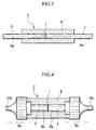
- Figs. 3 and 4 show examples of light-transmission-type optical fuse systems using the optical fuse of the present invention.
- an optical fiber 2 with a fiber core 2a and an optical fiber 5 with a fiber core 5a are held within a holder pipe 6 so that their ends face each other.
- the optical fuse 1 of the present invention is located between the ends of the optical fibers 2 and 5.
- the optical fuse 1 may be attached to one of the ends of the optical fibers 2 and 5, for example, to the end of the optical fiber 5 as shown in Fig. 8.
- a pair of the optical fibers 2 and 5 are held by a pair of ferrules 8a and 8b, and the optical fuse 1 is attached to one of the optical fibers 2 and 5, for example, to the end of the optical fiber 5.
- the optical fibers 2 and 5 are held within a holder pipe 6 and are connected via fiber connectors 9a and 9b to optical fibers 10a and 10b.
- the optical fuse component may be formed by various appropriate processes, for example, by a deposition process such as vacuum deposition and sputtering, a coating process, or a lamination process.
- a deposition process such as vacuum deposition and sputtering, a coating process, or a lamination process.
- the optical fuse comprises a dielectric thermally sensitive degradable material layer 11 and a light heatable material layer 12 formed thereon.
- the thermally sensitive degradable material layer 11 may be attached to a base 13, forming an optical fuse complex 14.
- the light heatable material layer 12 may be attached to the base 13, forming an optical fuse complex 34.
- the thickness of the thermally sensitive degradable material layer and the light heatable material layer are determined, depending on the wavelengths of the light and on the material of the optical fuse.
- the thickness of the light heatable material layer is in a range of 10 to 100 nm, and more preferably, in a range of 50 to 100 nm.
- the thickness of the thermally sensitive degradable material layer is in a range of 100 to 10000 nm, and more preferably, in a range of 100 to 1000 nm. To reduce optical loss under normal conditions, the thicknesses of these layers preferably are as thin as possible.
- the layer sequence of the light heatable material layer and the thermally sensitive degradable material layer is not limited to the above embodiments, and any one of the two layers may be positioned at the beam entering side.
- the light heatable material layer which is a metal layer with high reflectance (for example, Al), may be positioned at the beam entering side.
- the base preferably is formed of a transparent material such as glass, quartz, or fluorite.
- the end of the optical fiber attached to the fuse works as the base.
- the base is unnecessary.
- a plurality of the light heatable material layers 12 and a plurality of the thermally sensitive degradable material layers 11 may be alternatively stacked, and this layered body is disposed on the base 13, forming an optical fuse complex 44.
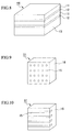
- spots of light heatable portions 15 which contain the light heatable material may be patterned as desired on a thermally sensitive degradable film 16 containing the thermally sensitive degradable material.
- the shapes, sizes, patterns, and distances of the spots may be appropriately modified.
- the light heatable portions 15 may be strips arranged on the thermally sensitive degradable film 16.
- the strip light heatable portions 15 may be straight, wavy, or zigzags. The sizes, patterns, and distances of the strips may be appropriately modified.
- the light heatable portion 15 may have, for example, a grid shape as desired on the thermally sensitive degradable film 16.
- the shape of the light heatable portion 15 is not limited to a grid shape, and may form other shapes such as a mesh shape. The shapes, sizes, and positions of the grids may be appropriately modified.
- the light heatable portions causes a small optical loss to beam with a low light intensity
- the total optical loss can be reduced, because the areas of the thermally sensitive degradable portions are large and the optical loss due to light absorption by the theremo-sensitive degradable portions becomes low.
- the threshold value of the optical fuse can be adjusted in consideration of the light surge to be controlled.
- the light heatable portions 15 may be a number of particles of the light heatable material, which are distributed in the thermally sensitive degradable portion 16.
- This optical fuse 1 may be layered on the base 13, forming an optical fuse complex 71.
- the sizes, shapes, distribution density, and distribution range of the light heatable portions 15 may be appropriately determined.
- a two-source deposition device may be used to manufacture the optical fuse of Fig. 12.
- the thermally sensitive degradable material (dielectric material) is evaporated at a high evaporation rate from one evaporation source to the base
- the light heatable material (metal, or semiconductor) is evaporated at a low evaporation rate from the other evaporation source, thus diffusing the particles of the light heatable material into the evaporated layer of the thermally sensitive degradable material.
- a sol-gel film which contains the light heatable material and the thermally sensitive degradable material may be heated, depositing the light heatable material (for example, metal) in clusters.
- the optical fuse of the second embodiment according to the present invention comprises a dielectric metal compound containing metal atoms and an organic group combined therewith and having transparency and reflectivity.
- the metal atoms generate heat, depending on the specified light intensity of incident beam, and degenerate or decompose the dielectric metal compound, which loses or reduces its transparency and reflectivity.
- the dielectric metal compound may be a complex compound of metal atoms with the organic group.
- the metal atom may be Al, Pd, Ge, or In which absorb light at predetermined wavelengths and generate heat.
- the complex compound may be Pd complex with polyvinyl alcohol (hereinafter referred to as Pd-PVA), Ge complex with phthalocyanine, Cl In complex with phthalocyanine, Mo complex with phthalocyanine, Ni complex with phthalocyanine, Mn complex with phthalocyanine, Pt complex with phthalocyanine, Ti complex with phthalocyanine, V complex with phthalocyanine, Cu complex with phthalocyanine, or Si complex with a copolymer of phthalocyanine-methyl methacrylate.
- the optical fuse of the second embodiment may be a film with a single layer.
- the second embodiment of the optical fuse utilizes a thermally sensitive degradable organic material, for example, a thermally sensitive organometallic compound such as complex in which, for example, metal atoms of the light heatable material are introduced into a dielectric organic material.
- the complex absorbs the light beam, generates heat, and is degraded, converted, or decomposed, reducing or losing its transparency or reflectivity.
- Fig. 13 shows the second embodiment of the optical fuse 81 of a single layer, which may be stacked on a base 13, forming an optical fuse complex 84 if necessary.
- Figs. 14 and 15 show a characteristic evaluator for the light-transmission-type optical fuse.
- the optical fuse is positioned between the optical fibers 2 and 5 facing each other in the evaluator 17.
- a Pd-PVA solution is applied to one of the ends of the optical fibers, and is dried and solidified at a room temperature all day, forming a film optical fuse with thickness of 5 ⁇ m.
- the other end of the optical fiber is disposed to face the optical fuse, and the fibers are connected to each other by a connector joint, thus forming an optical system.
- the optical fuse film is in contact with the ends of the optical fibers 2 and 5.
- a laser source 18 which emits a laser beam at a wavelength of 1.19 ⁇ m is connected to an optical fiber 19 in which the laser beam travels.
- the optical fiber 19 is branched at a coupler (not shown) to input 99% of the incident laser beam into a branched optical fiber 20 and to input 1% of the incident laser beam into another branched optical fiber 21 for monitoring the light intensity of the incident beam.
- the branched optical fiber 20 is connected to a measurement device 17 which includes the optical fuse shown in Fig. 19.
- the branched optical fibers 70 and 71 are connected to a power meter 22 and an x-y plotter 23. The light intensities of the beam entering the optical fuse and of the beam leaving the optical fuse are measured while changing the output from the laser source.
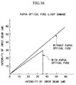
- Fig. 16 shows the results of the measurements, and is a graph showing the relationship between the light intensities of the beam entering the optical fuse to and the beam leaving the optical fuse.
- the abscissa represents the light intensity of the entering beam
- the ordinate represents the light intensity of the leaving beam.
- the graph shows a comparative example which does not include Pd-PVA optical fuse.
- Pd-PVA optical fuse is set between the fibers, an optical fusing action is found for a light intensity of the entering beam of 36 mW.
- the threshold value which causes the optical fusing action may be adjusted by changing the film thickness and the film processing conditions (for example, the solidification temperature).
- Fig. 17 shows the structure of the optical system using the optical fuse of a third embodiment according to the present invention.
- the optical fuse system 101 has a light input device 111 for inputting the signal beam 102 and a light output device 112 for outputting the signal beam 102.
- the light input device 111 and the light output device 112 are disposed on the same optical axis.
- a film 106 is provided on the optical axis of the input signal beam 102 between the light input device 111 and the light output device 112, and is inclined with respect to the optical axis at a predetermined angle.
- the angle of the film 106 is adjusted so as to set the transparency to above 90 percent and the reflectance to several percent.
- Most of the entering signal beam 102 may be transmitted through the film 106 and is output as a transmitted beam from the beam output device 112.
- Reference numeral 105 denotes a photo detector which receives beam 103 reflected by the film 106.
- the film 106 irreversibly changes its transparency and reflectivity when the intensity (power) of the incident beam exceeds a predetermined value. That is, the film 106 reduces its transparency to several percent and slightly increases its reflectivity in response to the incident beam with an excessive intensity (power).
- Fig. 18 shows the relationship between the intensity of the beam input to the light input device 111, the intensity of the beam output from the light output device 112, and the intensity of the reflected beam 103 detected by the photo detector 105.
- reference character P1 represents a threshold intensity value at which the transparency and the reflectivity are sharply changed.
- the transparency of the film 106 is sharply reduced so that the light output device 112 outputs little of the beam while the intensity of the reflected beam detected by the photo detector is increased because the reflectivity of the film is slightly increased.
- the transparency of the film 106 is reduced, to intercept the signal beam, decreasing the output of the light surge, and preventing a subsequent optical device (not shown) from being damaged.
- the optical fuse intercepts the signal before it is output in response to the input of the signal beam with intensity of more than the predetermined value, the reflectivity of the film 106 is increased, and the intensity of the reflected beam 103 is increased.
- the photo detector 105 detects the increased intensity of the reflected beam, and a user can know that the optical fuse system 101 should be exchanged, based on the interception of the output from the optical fuse system.
- the present inventor manufactured the optical fuse system 101 and conducted the experiment, which is described below.
- the light input device 111 and the light output device 112 are distributed shift fibers (DSF), and the photo detector 105 is a InGaAs-PIN photo diode.
- the film 106 has a multi-layered structure of SiO 2 /TiO 2 formed onto a glass substrate by deposition.
- the light output device 112 is located to the beam output side of the film 106.
- the transparency of the film 106 is 99.0 percent, and the reflectivity is 1 percent.
- the film 106 In response to the normal signal beam 102 at a wavelength of 1.55 ⁇ m and intensity (power) of 0.8 W, the film 106 does not change its transparency and reflectivity.
- the insertion loss of the optical fuse 101 is 3dB, and the intensity of the reflected beam is 0.01 mW.
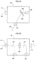
- Fig. 19 shows the structure of an optical fuse system of the fourth embodiment according to the present invention.
- the fourth embodiment differs from the third embodiment only insofar as a light output device 112 receives a beam reflected by a film 106 and that the photo detector 105 is disposed on an optical axis of the signal beam 102 and receives the beam transmitted through the film 106.
- the angle of the film 106 is set to a total reflection angle with respect to the optical axis of the incident signal beam 102. That is, the transparency and the reflectance of the fourth embodiment differ from those of the third embodiment.
- the film 106 has characteristics similar to those shown in Fig. 18, the film 106 is disposed so as to set the reflectance to 90 percent and the transparency to several percent.
- the intensity of the reflected beam 103 is increased in proportion to the increased intensity of the input signal beam.
- the reflectance is reduced and the transparency is slightly increased.
- the optical fuse of the second embodiment is advantageous when the optical axes cannot be arranged in a straight line. Further, because the photo detector 105 detects the beam transmitted through the film 106, a user can know that the optical fuse 101 should be exchanged, based on the interception of the signal from the optical fuse 101.
- Fig. 20 shows the structure of an optical fuse system using the optical fuse of the fifth embodiment according to the present invention.
- the film 106 is not inclined with respect to the optical axis of a signal beam 102.
- photo couplers 107 intervene between the light input device and the film 106 and between the film 106 and the light output device 112 and are connected to the photo detectors 105.
- the film 106 must reduce its transparency to close the transmission path when a light surge enters the film 106, and the reflection characteristic is not important.
- the photo detectors 105 detect the signal beam 102 from the light input device 111 and the beam transmitted through the film 106. That is, the photo detectors 105 monitor the input and output beams through the optical fuse. When the normal signal beam enters the optical fuse, the photo detectors 105 detect both beams. When the transmission path is closed in response to the light surge entering the optical fuse, the input side photo detector detects the beam while the output side photo detector detects no beam. Thus, by monitoring the outputs from the photo detectors 105, a user can know that the optical fuse has closed the transmission path. Because the branching ratios of the photo couplers 7 are high, the photo detectors are prevented from being damaged when a light surge enters the optical fuse.
- Fig. 21 shows the structure of an optical fuse system of the sixth embodiment according to the present invention.
- the sixth embodiment differs from the fifth embodiment only insofar as the film 106 is inclined at a predetermined angle with respect to an optical axis of a signal beam 102, the light output device 112 is disposed so as to receive the signal beam 102 entering and reflected by the film 106, and the photo detector 107 is disposed depending on the position of the light output device 112. That is, the photo coupler 107 is disposed between the film 106 and the light output device 112 and on an optical axis of the reflected beam (output beam) 103.
- the film 106 must reduce its reflectance to close the transmission path, and the transparency of the film 106 is not important.
- the photo detectors 105 detect the signal beam 102 input from the light input device 111 and the beam reflected by the film 106. That is, the photo detectors 105 monitors the input and output beams through the optical fuse. When a normal signal beam enters the optical fuse, the photo detectors 105 detect both beams. When the transmission path is closed in response to a light surge entering the optical fuse, the input side photo detector detects the beam while the output side photo detector detects no beam. Thus, by monitoring the outputs from the photo detectors 105, a user can know that the optical fuse has closed the transmission path. Because the branching ratios of the photo couplers 7 are high, the photo detectors are prevented from being damaged when a light surge enters the optical fuse.
- the film 106 is a multi-layered structure of SiO 2 /TiO 2
- the present invention is not limited to these embodiments, and MgF 2 , Ce, Si, Ge, and oxide (dielectric material) thereof may be deposited.
- the optical fuse of the present invention comprises: at least one light heatable portion for receiving anincident beam, and at least one thermally sensitive degradable portion with transparency and reflectivity, positioned in contact with the light heatable portion.
- the light heatable portion contains a light heatable material which generates heat depending on a specified light intensity of the incident beam.
- the thermally sensitive degradable portion contains a thermally sensitive degradable material which loses or reduces its transparency ad reflectivity, depending on the heat generated by the light heatable portion when the light intensity of the incident beam exceeds a threshold value.
Landscapes
- Physics & Mathematics (AREA)
- Nonlinear Science (AREA)
- General Physics & Mathematics (AREA)
- Optics & Photonics (AREA)
- Optical Modulation, Optical Deflection, Nonlinear Optics, Optical Demodulation, Optical Logic Elements (AREA)
- Compositions Of Macromolecular Compounds (AREA)
Applications Claiming Priority (4)
| Application Number | Priority Date | Filing Date | Title |
|---|---|---|---|
| JP7075198 | 1998-03-19 | ||
| JP7075198A JP3169885B2 (ja) | 1998-03-19 | 1998-03-19 | 光ヒューズ |
| JP10084027A JPH11281842A (ja) | 1998-03-30 | 1998-03-30 | 光ヒューズ、光ヒューズ複合体及びそれらを含む光ヒューズ装置 |
| JP8402798 | 1998-03-30 |
Publications (2)
| Publication Number | Publication Date |
|---|---|
| EP0943954A2 true EP0943954A2 (de) | 1999-09-22 |
| EP0943954A3 EP0943954A3 (de) | 2001-06-06 |
Family
ID=26411884
Family Applications (1)
| Application Number | Title | Priority Date | Filing Date |
|---|---|---|---|
| EP99302152A Withdrawn EP0943954A3 (de) | 1998-03-19 | 1999-03-19 | Optische Sicherung |
Country Status (2)
| Country | Link |
|---|---|
| US (1) | US6218658B1 (de) |
| EP (1) | EP0943954A3 (de) |
Cited By (8)
| Publication number | Priority date | Publication date | Assignee | Title |
|---|---|---|---|---|
| WO2002050587A1 (en) * | 2000-12-20 | 2002-06-27 | Corning Incorporated | Photothermal optical signal limiter |
| WO2004053442A1 (en) * | 2002-12-08 | 2004-06-24 | Kilolambda Technologies Ltd. | Optical power limiting devices and a method for protecting imaging and non-imaging sensors |
| WO2005050281A1 (ja) | 2003-11-18 | 2005-06-02 | National Institute For Materials Science | 光ヒューズおよび光ヒューズ作製用部品 |
| EP1483612A4 (de) * | 2002-03-13 | 2011-03-16 | Kilolambda Tech Ltd | Schalteinrichtung und verfahren für optische energie |
| WO2011031641A3 (en) * | 2009-09-09 | 2011-06-23 | Schlumberger Canada Limited | Dissolvable connector guard |
| WO2012123371A1 (en) * | 2011-03-11 | 2012-09-20 | University of Maribor | Optical fuse devices, optical fiber lines and methods of manufacturing same |
| US8478087B2 (en) | 2002-01-10 | 2013-07-02 | Kilolambda Technologies Ltd. | Optical limiter |
| US8923666B2 (en) | 2012-05-16 | 2014-12-30 | International Business Machines Corporation | Electrically controlled optical fuse and method of fabrication |
Families Citing this family (11)
| Publication number | Priority date | Publication date | Assignee | Title |
|---|---|---|---|---|
| JP4692696B2 (ja) * | 2000-09-08 | 2011-06-01 | 三菱瓦斯化学株式会社 | 光学材料用樹脂組成物 |
| WO2004005374A1 (ja) * | 2002-07-08 | 2004-01-15 | Mitsubishi Gas Chemical Company, Inc. | 重合性組成物、それからなる光学材料、及びその製造方法 |
| US20100061680A1 (en) * | 2007-01-31 | 2010-03-11 | Ram Oron | Resettable optical fuse |
| US20110170159A1 (en) * | 2008-06-24 | 2011-07-14 | Kilolambda Technologies Ltd. | Light limiting window |
| US8233758B2 (en) | 2010-03-11 | 2012-07-31 | Kilolambda Technologies Ltd. | Nanotube based optical fuse device and method |
| US8463090B2 (en) | 2010-03-11 | 2013-06-11 | Kilolambda Technologies Ltd. | Nanotube based optical fuse device and method |
| EP2541699A3 (de) | 2011-06-30 | 2014-01-22 | Kilolambda Technologies Ltd. | Nanoröhrchenbasierte optische Sicherungsvorrichtung und Verfahren |
| CA2922421C (en) | 2013-10-07 | 2018-03-06 | Halliburton Energy Services, Inc. | Power limiting methods for use with optical systems in hazardous area locations |
| US10439733B2 (en) | 2014-01-13 | 2019-10-08 | The Johns Hopkins University | Fiber optic circuit breaker |
| US11729535B2 (en) | 2020-03-30 | 2023-08-15 | British Telecommunications Public Limited Company | Optical switch and optical routing method and system |
| US11774785B2 (en) | 2020-03-30 | 2023-10-03 | British Telecommunications Public Limited Company | Optical limiter and method for limiting radiant flux |
Family Cites Families (10)
| Publication number | Priority date | Publication date | Assignee | Title |
|---|---|---|---|---|
| JPS61125882A (ja) * | 1984-11-22 | 1986-06-13 | Victor Co Of Japan Ltd | 光記録媒体 |
| US4737000A (en) | 1986-07-09 | 1988-04-12 | Hughes Aircraft Company | Apparatus for diverting electromagnetic radiation from sensitive optical apparatus |
| US4933929A (en) * | 1987-06-29 | 1990-06-12 | Nec Corporation | Wavelength multiplexed optical transmitter for generating constant-amplitude angle-modulated beams to eliminate phase noise in adjacent transmission channels |
| JPH01117380A (ja) | 1987-10-30 | 1989-05-10 | Nec Corp | 損傷検出機能付きレーザ発振器 |
| US5017769A (en) * | 1990-03-26 | 1991-05-21 | Hughes Aircraft Company | Surface particulate laser power limiter which generates a plasma |
| JPH04155937A (ja) | 1990-10-19 | 1992-05-28 | Fujitsu Ltd | レーザ光のオーバーパワーモニタ方法 |
| US5153425A (en) * | 1990-12-24 | 1992-10-06 | United Technologies Corporation | Broadband optical limiter with sacrificial mirror to prevent irradiation of a sensor system by high intensity laser radiation |
| GB2290388A (en) * | 1994-06-07 | 1995-12-20 | British Aerospace | Optical element and system responsive to light intensity |
| JPH09146056A (ja) | 1995-11-20 | 1997-06-06 | Oki Electric Ind Co Ltd | 光フューズ及び光素子保護装置 |
| JPH09171103A (ja) * | 1995-12-19 | 1997-06-30 | Nikon Corp | 光学部品の保護器具 |
-
1999
- 1999-03-17 US US09/271,302 patent/US6218658B1/en not_active Expired - Fee Related
- 1999-03-19 EP EP99302152A patent/EP0943954A3/de not_active Withdrawn
Cited By (13)
| Publication number | Priority date | Publication date | Assignee | Title |
|---|---|---|---|---|
| US6415075B1 (en) | 2000-12-20 | 2002-07-02 | Corning Incorporated | Photothermal optical signal limiter |
| WO2002050587A1 (en) * | 2000-12-20 | 2002-06-27 | Corning Incorporated | Photothermal optical signal limiter |
| US8478087B2 (en) | 2002-01-10 | 2013-07-02 | Kilolambda Technologies Ltd. | Optical limiter |
| EP1483612A4 (de) * | 2002-03-13 | 2011-03-16 | Kilolambda Tech Ltd | Schalteinrichtung und verfahren für optische energie |
| WO2004053442A1 (en) * | 2002-12-08 | 2004-06-24 | Kilolambda Technologies Ltd. | Optical power limiting devices and a method for protecting imaging and non-imaging sensors |
| WO2005050281A1 (ja) | 2003-11-18 | 2005-06-02 | National Institute For Materials Science | 光ヒューズおよび光ヒューズ作製用部品 |
| EP1686411A4 (de) * | 2003-11-18 | 2010-02-17 | Nat Inst For Materials Science | Optische schmelzverbindung und komponente zur herstellung einer optischen schmelzverbindung |
| WO2011031641A3 (en) * | 2009-09-09 | 2011-06-23 | Schlumberger Canada Limited | Dissolvable connector guard |
| US8113290B2 (en) | 2009-09-09 | 2012-02-14 | Schlumberger Technology Corporation | Dissolvable connector guard |
| WO2012123371A1 (en) * | 2011-03-11 | 2012-09-20 | University of Maribor | Optical fuse devices, optical fiber lines and methods of manufacturing same |
| US8942531B2 (en) | 2011-03-11 | 2015-01-27 | University of Maribor | Optical fuse devices, optical fiber lines, and methods of manufacturing same |
| US8923666B2 (en) | 2012-05-16 | 2014-12-30 | International Business Machines Corporation | Electrically controlled optical fuse and method of fabrication |
| US9417501B2 (en) | 2012-05-16 | 2016-08-16 | Globalfoundries Inc. | Electrically controlled optical fuse and method of fabrication |
Also Published As
| Publication number | Publication date |
|---|---|
| EP0943954A3 (de) | 2001-06-06 |
| US6218658B1 (en) | 2001-04-17 |
Similar Documents
| Publication | Publication Date | Title |
|---|---|---|
| US6218658B1 (en) | Optical fuse | |
| JP3325825B2 (ja) | 3次元周期構造体及びその作製方法並びに膜の製造方法 | |
| US7245644B2 (en) | Semiconductor monolithic integrated optical transmitter | |
| US8115998B2 (en) | In-line optical isolator | |
| JP2971551B2 (ja) | 光増幅器―光検出器デバイス | |
| US20050063659A1 (en) | Method and apparatus for decreasing signal propagation delay in a waveguide | |
| McKee et al. | High quality wavelength tuned multiquantum well GaInAs/GaInAsP lasers fabricated using photoabsorption induced disordering | |
| JP5344393B2 (ja) | 超伝導単一光子検出器の部品の実装方法 | |
| JPH11281842A (ja) | 光ヒューズ、光ヒューズ複合体及びそれらを含む光ヒューズ装置 | |
| WO1999017472A1 (fr) | Dispositif et procede d'attenuation de l'intensite optique | |
| WO2014021916A1 (en) | Sacrificial limiter filter | |
| US7488925B2 (en) | Light control apparatus having a device for controlling the input signal light of an optical transmission path | |
| Dubovitsky et al. | Gain saturation properties of a polarization insensitive semiconductor amplifier implemented with tensile and compressive strain quantum wells | |
| JPH01502614A (ja) | 光信号処理デバイス | |
| EP1317037A2 (de) | Optischer Verstärker | |
| Arnaud et al. | Spontaneous emission in semiconductor laser amplifiers | |
| Tanabe et al. | Characteristics of time-gated Raman amplification in GaP–AlGaP semiconductor waveguides | |
| US6870667B2 (en) | Optical amplifier | |
| JP2005191074A (ja) | 希土類元素添加半導体光増幅器及び光スイッチ | |
| JP3524068B2 (ja) | 半導体光吸収素子および半導体光吸収素子を応用したパルス光発生装置および光パルス整形方法 | |
| JPS617683A (ja) | 光電素子 | |
| Casale et al. | 1.55 µm hybrid waveguide laser made by ion-exchange and wafer bonding | |
| EP1039336A2 (de) | Vorrichtung mit einer optischen Funktion | |
| Tan et al. | Characterization and Optical Properties of Erbium doped As2S3 Films Prepared by Multi-layer Magnetron Sputtering | |
| Travers-Nabialek | Tantalum oxide anti-reflective thin films for C-band travelling-wave semiconductor optical amplifiers |
Legal Events
| Date | Code | Title | Description |
|---|---|---|---|
| PUAI | Public reference made under article 153(3) epc to a published international application that has entered the european phase |
Free format text: ORIGINAL CODE: 0009012 |
|
| AK | Designated contracting states |
Kind code of ref document: A2 Designated state(s): FR GB IT |
|
| AX | Request for extension of the european patent |
Free format text: AL;LT;LV;MK;RO;SI |
|
| PUAL | Search report despatched |
Free format text: ORIGINAL CODE: 0009013 |
|
| AK | Designated contracting states |
Kind code of ref document: A3 Designated state(s): AT BE CH CY DE DK ES FI FR GB GR IE IT LI LU MC NL PT SE |
|
| AX | Request for extension of the european patent |
Free format text: AL;LT;LV;MK;RO;SI |
|
| RIC1 | Information provided on ipc code assigned before grant |
Free format text: 7G 02F 1/35 A, 7G 02B 5/00 B |
|
| 17P | Request for examination filed |
Effective date: 20010504 |
|
| 17Q | First examination report despatched |
Effective date: 20010718 |
|
| AKX | Designation fees paid |
Free format text: FR GB IT |
|
| REG | Reference to a national code |
Ref country code: DE Ref legal event code: 8566 |
|
| STAA | Information on the status of an ep patent application or granted ep patent |
Free format text: STATUS: THE APPLICATION IS DEEMED TO BE WITHDRAWN |
|
| 18D | Application deemed to be withdrawn |
Effective date: 20011129 |