EP1317037A2 - Optischer Verstärker - Google Patents
Optischer Verstärker Download PDFInfo
- Publication number
- EP1317037A2 EP1317037A2 EP02026453A EP02026453A EP1317037A2 EP 1317037 A2 EP1317037 A2 EP 1317037A2 EP 02026453 A EP02026453 A EP 02026453A EP 02026453 A EP02026453 A EP 02026453A EP 1317037 A2 EP1317037 A2 EP 1317037A2
- Authority
- EP
- European Patent Office
- Prior art keywords
- light source
- source device
- laser element
- semiconductor laser
- excitation light
- Prior art date
- Legal status (The legal status is an assumption and is not a legal conclusion. Google has not performed a legal analysis and makes no representation as to the accuracy of the status listed.)
- Withdrawn
Links
Images


Classifications
-
- B—PERFORMING OPERATIONS; TRANSPORTING
- B82—NANOTECHNOLOGY
- B82Y—SPECIFIC USES OR APPLICATIONS OF NANOSTRUCTURES; MEASUREMENT OR ANALYSIS OF NANOSTRUCTURES; MANUFACTURE OR TREATMENT OF NANOSTRUCTURES
- B82Y20/00—Nanooptics, e.g. quantum optics or photonic crystals
-
- H—ELECTRICITY
- H01—ELECTRIC ELEMENTS
- H01S—DEVICES USING THE PROCESS OF LIGHT AMPLIFICATION BY STIMULATED EMISSION OF RADIATION [LASER] TO AMPLIFY OR GENERATE LIGHT; DEVICES USING STIMULATED EMISSION OF ELECTROMAGNETIC RADIATION IN WAVE RANGES OTHER THAN OPTICAL
- H01S3/00—Lasers, i.e. devices using stimulated emission of electromagnetic radiation in the infrared, visible or ultraviolet wave range
- H01S3/05—Construction or shape of optical resonators; Accommodation of active medium therein; Shape of active medium
- H01S3/06—Construction or shape of active medium
- H01S3/063—Waveguide lasers, i.e. whereby the dimensions of the waveguide are of the order of the light wavelength
- H01S3/067—Fibre lasers
- H01S3/06754—Fibre amplifiers
-
- H—ELECTRICITY
- H01—ELECTRIC ELEMENTS
- H01S—DEVICES USING THE PROCESS OF LIGHT AMPLIFICATION BY STIMULATED EMISSION OF RADIATION [LASER] TO AMPLIFY OR GENERATE LIGHT; DEVICES USING STIMULATED EMISSION OF ELECTROMAGNETIC RADIATION IN WAVE RANGES OTHER THAN OPTICAL
- H01S2303/00—Pumping wavelength
-
- H—ELECTRICITY
- H01—ELECTRIC ELEMENTS
- H01S—DEVICES USING THE PROCESS OF LIGHT AMPLIFICATION BY STIMULATED EMISSION OF RADIATION [LASER] TO AMPLIFY OR GENERATE LIGHT; DEVICES USING STIMULATED EMISSION OF ELECTROMAGNETIC RADIATION IN WAVE RANGES OTHER THAN OPTICAL
- H01S3/00—Lasers, i.e. devices using stimulated emission of electromagnetic radiation in the infrared, visible or ultraviolet wave range
- H01S3/09—Processes or apparatus for excitation, e.g. pumping
- H01S3/091—Processes or apparatus for excitation, e.g. pumping using optical pumping
- H01S3/094—Processes or apparatus for excitation, e.g. pumping using optical pumping by coherent light
- H01S3/094003—Processes or apparatus for excitation, e.g. pumping using optical pumping by coherent light the pumped medium being a fibre
-
- H—ELECTRICITY
- H01—ELECTRIC ELEMENTS
- H01S—DEVICES USING THE PROCESS OF LIGHT AMPLIFICATION BY STIMULATED EMISSION OF RADIATION [LASER] TO AMPLIFY OR GENERATE LIGHT; DEVICES USING STIMULATED EMISSION OF ELECTROMAGNETIC RADIATION IN WAVE RANGES OTHER THAN OPTICAL
- H01S3/00—Lasers, i.e. devices using stimulated emission of electromagnetic radiation in the infrared, visible or ultraviolet wave range
- H01S3/09—Processes or apparatus for excitation, e.g. pumping
- H01S3/091—Processes or apparatus for excitation, e.g. pumping using optical pumping
- H01S3/094—Processes or apparatus for excitation, e.g. pumping using optical pumping by coherent light
- H01S3/0941—Processes or apparatus for excitation, e.g. pumping using optical pumping by coherent light of a laser diode
- H01S3/09415—Processes or apparatus for excitation, e.g. pumping using optical pumping by coherent light of a laser diode the pumping beam being parallel to the lasing mode of the pumped medium, e.g. end-pumping
-
- H—ELECTRICITY
- H01—ELECTRIC ELEMENTS
- H01S—DEVICES USING THE PROCESS OF LIGHT AMPLIFICATION BY STIMULATED EMISSION OF RADIATION [LASER] TO AMPLIFY OR GENERATE LIGHT; DEVICES USING STIMULATED EMISSION OF ELECTROMAGNETIC RADIATION IN WAVE RANGES OTHER THAN OPTICAL
- H01S3/00—Lasers, i.e. devices using stimulated emission of electromagnetic radiation in the infrared, visible or ultraviolet wave range
- H01S3/14—Lasers, i.e. devices using stimulated emission of electromagnetic radiation in the infrared, visible or ultraviolet wave range characterised by the material used as the active medium
- H01S3/16—Solid materials
- H01S3/1601—Solid materials characterised by an active (lasing) ion
- H01S3/1603—Solid materials characterised by an active (lasing) ion rare earth
- H01S3/1608—Solid materials characterised by an active (lasing) ion rare earth erbium
-
- H—ELECTRICITY
- H01—ELECTRIC ELEMENTS
- H01S—DEVICES USING THE PROCESS OF LIGHT AMPLIFICATION BY STIMULATED EMISSION OF RADIATION [LASER] TO AMPLIFY OR GENERATE LIGHT; DEVICES USING STIMULATED EMISSION OF ELECTROMAGNETIC RADIATION IN WAVE RANGES OTHER THAN OPTICAL
- H01S5/00—Semiconductor lasers
- H01S5/02—Structural details or components not essential to laser action
- H01S5/028—Coatings ; Treatment of the laser facets, e.g. etching, passivation layers or reflecting layers
-
- H—ELECTRICITY
- H01—ELECTRIC ELEMENTS
- H01S—DEVICES USING THE PROCESS OF LIGHT AMPLIFICATION BY STIMULATED EMISSION OF RADIATION [LASER] TO AMPLIFY OR GENERATE LIGHT; DEVICES USING STIMULATED EMISSION OF ELECTROMAGNETIC RADIATION IN WAVE RANGES OTHER THAN OPTICAL
- H01S5/00—Semiconductor lasers
- H01S5/30—Structure or shape of the active region; Materials used for the active region
- H01S5/34—Structure or shape of the active region; Materials used for the active region comprising quantum well or superlattice structures, e.g. single quantum well [SQW] lasers, multiple quantum well [MQW] lasers or graded index separate confinement heterostructure [GRINSCH] lasers
- H01S5/343—Structure or shape of the active region; Materials used for the active region comprising quantum well or superlattice structures, e.g. single quantum well [SQW] lasers, multiple quantum well [MQW] lasers or graded index separate confinement heterostructure [GRINSCH] lasers in AIIIBV compounds, e.g. AlGaAs-laser, InP-based laser
- H01S5/3434—Structure or shape of the active region; Materials used for the active region comprising quantum well or superlattice structures, e.g. single quantum well [SQW] lasers, multiple quantum well [MQW] lasers or graded index separate confinement heterostructure [GRINSCH] lasers in AIIIBV compounds, e.g. AlGaAs-laser, InP-based laser with a well layer comprising at least both As and P as V-compounds
Definitions
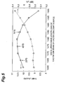
- Figure 6 is a graph illustrating the results of a test of output characteristic of an optical amplifier in the case where in particular the oscillation wavelength of the excitation beam is on the short wavelength side of 1480 nm; only the output power of the signal beam is plotted with respect to the oscillation wavelength of the excitation beam that is output from the semiconductor laser element.
- "[black diamond symbol]” indicates the output power (dBm) of the signal beam.
- the vertical axis indicates the amount of change ( ⁇ ) of the output power with respect to the output power of the signal beam when the oscillation wavelength of the excitation beam is 1480 nm.
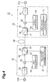
- the test was conducted under the following conditions with the optical amplifier shown in Figure 4.
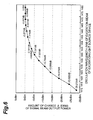
- an optical amplifier by setting the oscillation wavelength of the excitation light source device on the short wavelength side of 1480 nm, which is the peak wavelength of the gain in an erbium-doped optical fiber, it is possible to make the amount of change of gain in the erbium-doped optical fiber satisfactorily small with respect to the amount of change of oscillation wavelength, and the wavelength dependence of the gain in an erbium-doped optical fiber can thereby be made satisfactorily small.
- the difference between the gain in the erbium-doped optical fiber when the temperature of the semiconductor laser element is high and when it is low can therefore be made satisfactorily small.
- the oscillation wavelength on the short wavelength side of 1480 nm which is the peak wavelength of gain in an erbium-doped optical fiber
- the NF can be made satisfactorily small and the wavelength dependence of the NF can be made small.
Landscapes
- Engineering & Computer Science (AREA)
- Physics & Mathematics (AREA)
- Chemical & Material Sciences (AREA)
- Electromagnetism (AREA)
- Optics & Photonics (AREA)
- Nanotechnology (AREA)
- Plasma & Fusion (AREA)
- Biophysics (AREA)
- Crystallography & Structural Chemistry (AREA)
- Life Sciences & Earth Sciences (AREA)
- Lasers (AREA)
- Optical Communication System (AREA)
- Semiconductor Lasers (AREA)
Applications Claiming Priority (2)
| Application Number | Priority Date | Filing Date | Title |
|---|---|---|---|
| JP2001361133A JP2003163396A (ja) | 2001-11-27 | 2001-11-27 | 光増幅器 |
| JP2001361133 | 2001-11-27 |
Publications (2)
| Publication Number | Publication Date |
|---|---|
| EP1317037A2 true EP1317037A2 (de) | 2003-06-04 |
| EP1317037A3 EP1317037A3 (de) | 2005-07-06 |
Family
ID=19171841
Family Applications (1)
| Application Number | Title | Priority Date | Filing Date |
|---|---|---|---|
| EP02026453A Withdrawn EP1317037A3 (de) | 2001-11-27 | 2002-11-27 | Optischer Verstärker |
Country Status (3)
| Country | Link |
|---|---|
| EP (1) | EP1317037A3 (de) |
| JP (1) | JP2003163396A (de) |
| CN (1) | CN1422028A (de) |
Cited By (1)
| Publication number | Priority date | Publication date | Assignee | Title |
|---|---|---|---|---|
| EP2661794A4 (de) * | 2011-01-04 | 2014-07-16 | Ipg Photonics Corp | Verfahren zur stabilisierung der optischen ausgangsleistung eines faserlasers |
Families Citing this family (4)
| Publication number | Priority date | Publication date | Assignee | Title |
|---|---|---|---|---|
| JP2007288124A (ja) * | 2006-03-22 | 2007-11-01 | Nippon Telegr & Teleph Corp <Ntt> | 光ファイバ増幅器 |
| JP2009059938A (ja) * | 2007-08-31 | 2009-03-19 | Nippon Telegr & Teleph Corp <Ntt> | 光ファイバ増幅器 |
| JP2012080138A (ja) * | 2012-01-24 | 2012-04-19 | Nippon Telegr & Teleph Corp <Ntt> | 光ファイバ増幅器 |
| JP6417199B2 (ja) * | 2014-12-08 | 2018-10-31 | 浜松ホトニクス株式会社 | 量子カスケードレーザ装置 |
Family Cites Families (5)
| Publication number | Priority date | Publication date | Assignee | Title |
|---|---|---|---|---|
| JPS59177986A (ja) * | 1983-03-28 | 1984-10-08 | Matsushita Electric Ind Co Ltd | 半導体レ−ザの製造方法 |
| JPS59208886A (ja) * | 1983-05-13 | 1984-11-27 | Hitachi Ltd | 発光半導体装置 |
| JPH03217065A (ja) * | 1990-01-23 | 1991-09-24 | Toshiba Corp | レーザダイオード装置 |
| WO2001057976A1 (en) * | 2000-02-03 | 2001-08-09 | The Furukawa Electric Co., Ltd. | Semiconductor laser module and pumping light source comprising the same |
| AU2000233234A1 (en) * | 2000-03-03 | 2001-09-12 | Optical Technologies Italia S.P.A. | Optical amplifier and optical transmission system |
-
2001
- 2001-11-27 JP JP2001361133A patent/JP2003163396A/ja active Pending
-
2002
- 2002-11-27 EP EP02026453A patent/EP1317037A3/de not_active Withdrawn
- 2002-11-27 CN CN 02152744 patent/CN1422028A/zh active Pending
Cited By (1)
| Publication number | Priority date | Publication date | Assignee | Title |
|---|---|---|---|---|
| EP2661794A4 (de) * | 2011-01-04 | 2014-07-16 | Ipg Photonics Corp | Verfahren zur stabilisierung der optischen ausgangsleistung eines faserlasers |
Also Published As
| Publication number | Publication date |
|---|---|
| EP1317037A3 (de) | 2005-07-06 |
| CN1422028A (zh) | 2003-06-04 |
| JP2003163396A (ja) | 2003-06-06 |
Similar Documents
| Publication | Publication Date | Title |
|---|---|---|
| US6950452B2 (en) | Semiconductor laser module and method for simultaneously reducing relative intensity noise (RIN) and stimulated brillouin scattering (SBS) | |
| JP4090402B2 (ja) | 半導体光増幅器及びそれを用いた光モジュ−ル | |
| EP1246321B1 (de) | Mantelgepumpter 3-Niveau Faserlaser/Verstärker | |
| Joergensen et al. | 4 Gb/s optical wavelength conversion using semiconductor optical amplifiers | |
| US20170187168A1 (en) | Optical semiconductor device, semiconductor laser module, and optical fiber amplifier | |
| US6288833B1 (en) | Optical device | |
| JPH041614A (ja) | 光増幅装置 | |
| EP1085620A2 (de) | Laser, optische Verstärker und Verstärkungsverfahren | |
| JP2010232371A (ja) | 半導体光増幅素子 | |
| US6829285B2 (en) | Semiconductor laser device and method for effectively reducing facet reflectivity | |
| US20030091300A1 (en) | Semiconductor laser device, semiconductor laser module, Raman amplifier using the device or module, and method for forming a suitable current blocking layer | |
| EP1317037A2 (de) | Optischer Verstärker | |
| US6643308B2 (en) | Semiconductor laser device and method for suppressing injection current | |
| JP5505226B2 (ja) | 半導体光増幅器 | |
| Juodawlkis et al. | Packaged 1.5-$\mu $ m Quantum-Well SOA With 0.8-W Output Power and 5.5-dB Noise Figure | |
| US6870667B2 (en) | Optical amplifier | |
| US20030072342A1 (en) | Semiconductor laser device, semiconductor laser module, and optical fiber amplifer | |
| KR20040106676A (ko) | 라만 증폭원리를 이용한 이득 고정 반도체 광증폭기 | |
| US10511150B2 (en) | Wavelength-variable laser | |
| JP2002374037A (ja) | 半導体レーザモジュール、それを用いたファイバ増幅器と光通信システム | |
| JP6722829B2 (ja) | 単一チップ内に活性コア及びドープされたクラッドを有する固体光増幅器 | |
| GB2408146A (en) | Semiconductor laser device, semiconductor laser module, and optical fiber amplifier | |
| EP1233490A2 (de) | Halbleiterlasermodul und Phaserverstärker und optisches Kommunikationssytem unter Verwendung desselben | |
| JP3725498B2 (ja) | 半導体レーザ装置、半導体レーザモジュールおよびこれを用いたラマン増幅器ならびにwdm通信システム | |
| CN114792924A (zh) | 具有直通泵浦激光器的掺杂光纤放大器 |
Legal Events
| Date | Code | Title | Description |
|---|---|---|---|
| PUAI | Public reference made under article 153(3) epc to a published international application that has entered the european phase |
Free format text: ORIGINAL CODE: 0009012 |
|
| AK | Designated contracting states |
Designated state(s): AT BE BG CH CY CZ DE DK EE ES FI FR GB GR IE IT LI LU MC NL PT SE SK TR |
|
| AX | Request for extension of the european patent |
Extension state: AL LT LV MK RO SI |
|
| PUAL | Search report despatched |
Free format text: ORIGINAL CODE: 0009013 |
|
| AK | Designated contracting states |
Kind code of ref document: A3 Designated state(s): AT BE BG CH CY CZ DE DK EE ES FI FR GB GR IE IT LI LU MC NL PT SE SK TR |
|
| AX | Request for extension of the european patent |
Extension state: AL LT LV MK RO SI |
|
| AKX | Designation fees paid | ||
| STAA | Information on the status of an ep patent application or granted ep patent |
Free format text: STATUS: THE APPLICATION IS DEEMED TO BE WITHDRAWN |
|
| 18D | Application deemed to be withdrawn |
Effective date: 20060110 |
|
| REG | Reference to a national code |
Ref country code: DE Ref legal event code: 8566 |