EP0948023B1 - Plasma-Anzeigetafel - Google Patents
Plasma-Anzeigetafel Download PDFInfo
- Publication number
- EP0948023B1 EP0948023B1 EP99106496A EP99106496A EP0948023B1 EP 0948023 B1 EP0948023 B1 EP 0948023B1 EP 99106496 A EP99106496 A EP 99106496A EP 99106496 A EP99106496 A EP 99106496A EP 0948023 B1 EP0948023 B1 EP 0948023B1
- Authority
- EP
- European Patent Office
- Prior art keywords
- glass layer
- ribs
- base glass
- light
- display panel
- Prior art date
- Legal status (The legal status is an assumption and is not a legal conclusion. Google has not performed a legal analysis and makes no representation as to the accuracy of the status listed.)
- Expired - Lifetime
Links
Images




Classifications
-
- H—ELECTRICITY
- H01—ELECTRIC ELEMENTS
- H01J—ELECTRIC DISCHARGE TUBES OR DISCHARGE LAMPS
- H01J11/00—Gas-filled discharge tubes with alternating current induction of the discharge, e.g. alternating current plasma display panels [AC-PDP]; Gas-filled discharge tubes without any main electrode inside the vessel; Gas-filled discharge tubes with at least one main electrode outside the vessel
- H01J11/20—Constructional details
- H01J11/34—Vessels, containers or parts thereof, e.g. substrates
-
- H—ELECTRICITY
- H01—ELECTRIC ELEMENTS
- H01J—ELECTRIC DISCHARGE TUBES OR DISCHARGE LAMPS
- H01J11/00—Gas-filled discharge tubes with alternating current induction of the discharge, e.g. alternating current plasma display panels [AC-PDP]; Gas-filled discharge tubes without any main electrode inside the vessel; Gas-filled discharge tubes with at least one main electrode outside the vessel
- H01J11/10—AC-PDPs with at least one main electrode being out of contact with the plasma
- H01J11/12—AC-PDPs with at least one main electrode being out of contact with the plasma with main electrodes provided on both sides of the discharge space
-
- H—ELECTRICITY
- H01—ELECTRIC ELEMENTS
- H01J—ELECTRIC DISCHARGE TUBES OR DISCHARGE LAMPS
- H01J11/00—Gas-filled discharge tubes with alternating current induction of the discharge, e.g. alternating current plasma display panels [AC-PDP]; Gas-filled discharge tubes without any main electrode inside the vessel; Gas-filled discharge tubes with at least one main electrode outside the vessel
- H01J11/20—Constructional details
- H01J11/34—Vessels, containers or parts thereof, e.g. substrates
- H01J11/36—Spacers, barriers, ribs, partitions or the like
-
- H—ELECTRICITY
- H01—ELECTRIC ELEMENTS
- H01J—ELECTRIC DISCHARGE TUBES OR DISCHARGE LAMPS
- H01J11/00—Gas-filled discharge tubes with alternating current induction of the discharge, e.g. alternating current plasma display panels [AC-PDP]; Gas-filled discharge tubes without any main electrode inside the vessel; Gas-filled discharge tubes with at least one main electrode outside the vessel
- H01J11/20—Constructional details
- H01J11/34—Vessels, containers or parts thereof, e.g. substrates
- H01J11/44—Optical arrangements or shielding arrangements, e.g. filters, black matrices, light reflecting means or electromagnetic shielding means
-
- H—ELECTRICITY
- H01—ELECTRIC ELEMENTS
- H01J—ELECTRIC DISCHARGE TUBES OR DISCHARGE LAMPS
- H01J2211/00—Plasma display panels with alternate current induction of the discharge, e.g. AC-PDPs
- H01J2211/20—Constructional details
- H01J2211/34—Vessels, containers or parts thereof, e.g. substrates
- H01J2211/36—Spacers, barriers, ribs, partitions or the like
- H01J2211/366—Spacers, barriers, ribs, partitions or the like characterized by the material
-
- H—ELECTRICITY
- H01—ELECTRIC ELEMENTS
- H01J—ELECTRIC DISCHARGE TUBES OR DISCHARGE LAMPS
- H01J2211/00—Plasma display panels with alternate current induction of the discharge, e.g. AC-PDPs
- H01J2211/20—Constructional details
- H01J2211/34—Vessels, containers or parts thereof, e.g. substrates
- H01J2211/38—Dielectric or insulating layers
-
- H—ELECTRICITY
- H01—ELECTRIC ELEMENTS
- H01J—ELECTRIC DISCHARGE TUBES OR DISCHARGE LAMPS
- H01J2211/00—Plasma display panels with alternate current induction of the discharge, e.g. AC-PDPs
- H01J2211/20—Constructional details
- H01J2211/34—Vessels, containers or parts thereof, e.g. substrates
- H01J2211/44—Optical arrangements or shielding arrangements, e.g. filters or lenses
- H01J2211/444—Means for improving contrast or colour purity, e.g. black matrix or light shielding means
Definitions
- the present invention relates to a display element and plasma display panel preferably used for an image display of television and computer.
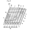
- a conventional AC plasma display panel is illustrated in part in Fig. 5.
- a plurality of scanning electrode 4 and sustaining electrode 5 that are parallel to each other are formed on a first insulative substrate 1.
- the scanning electrodes 4 and the sustaining electrode 5 are covered with a dielectric layer 2 and a protection layer 3.
- a second insulative substrate 6 which is facing the first insulative substrate 1
- a plurality of data electrodes 7 that are parallel to each other are formed orthogonally to the scanning electrodes 4 and the sustaining electrodes 5.
- the data electrodes 7 are covered with a base glass layer 8 made of white material.
- a plurality of ribs 9 also made of white material are formed on the base glass layer 8.
- the ribs 9 are arranged so that each cooperates with the neighboring rib to define a channel adjacent to and along the data electrode 7.
- a phosphor 10 is provided in each channel to cover opposing side walls of the neighboring ribs and a part of the base glass layer exposed between the neighboring ribs, so that a discharge chamber 11 is defined on and along phosphor 10.
- the neighboring scanning and sustaining electrodes, 4 and 5 are paired so that an electric discharge can be occurred with an aid of the data electrode 7 in a restricted region of the discharge chamber 11.
- the discharge generates ultraviolet light that excites an adjacent part of the phosphor 10.
- the excited portion of the phosphor 10 emits visual light for displaying an image.
- each area where the data electrode 7 crosses the pair of scanning and sustaining electrodes, 4 and 5, defines a discharge cell 12 as hatched in Fig. 5.
- each of the ribs 9 constitute red phosphor 10R, green phosphor 10G, and blue phosphor 10B, respectively, in this order.
- Selected and used for the white material of both the base glass layer 8 and ribs 9 is, for example, a white glass reflective to the visual light.
- a thickness of the base glass layer 8 is as small as possible to minimize a voltage for driving the data electrodes 7.
- the base glass layer has a thickness of about 10 to 15 micrometers.
- a thickness of the ribs 9 is as small as possible to maximize an opening area of the discharge chamber 11.
- each of the ribs 9 has a thickness of about 20 to 60 micrometers.
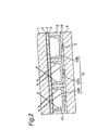
- Fig. 6 illustrating a cross sectional view taken along lines VI-VI in Fig. 5, descriptions will be made to functions of the base glass layer 8 and ribs 9.
- Fig. 6 shows that only the green phosphor 10G is excited for emitting green light.
- a few light passes are illustrated in the drawing, which passes may not be depicted correctly from an optical standpoint.
- ultraviolet light generated by the discharge between the scanning and sustaining electrodes, 4 and 5, with an aid of the data electrode 7 excites the green phosphor 10G.
- part of the green light emitted from a surface of the green phosphor 10G is reflected at surfaces of the base glass layer 8 and ribs 9 and then transmitted through the first substrate 1 for displaying.
- the base glass layer 8 and the ribs 9 are made of white material, for example, white glass, reflective to the visual light.
- the white material can reflect only about 50 to 60 percent of the visual light. Then, the structure does not improve the brightness of the panel so much. In addition, remaining 40 to 50 percent of the light is transmitted into the white material where it may be damped. Disadvantageously, several to several tens percent of the light can pass the white material, which may provide adverse effect.
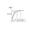
- Fig. 7 is a graph illustrating a relationship between thickness of the phosphor and brightness of light from the display panel.
- thickness-brightness characteristic curve A is for the base glass layer 8 and rib 9 having reflectance of 60 percent
- curve B for base glass layer and ribs having reflectance of zero percent.
- This graph shows that if the thickness is lower than about 15 micrometers the brightness increases with the thickness due to the reflected light from the base glass layer 8 and the ribs 9 and if the thickness is greater than about 25 micrometers the brightness no longer increase too much. This means that it is effective to increase the thickness of the phosphor for increasing the brightness of the panel.
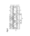
- Fig. 8 is a cross sectional view taken along lines VI-VI in Fig. 5, another descriptions will be made to the adverse effect of the transmitted light through the base glass layer and ribs.
- Fig. 8 illustrates that the discharge cells 12 of the red and green phosphors, 10R and 10G, are excited to emit respective light, but the discharge cell 12 of the blue phosphor 10B is not excited.
- the discharge cell 12 of the blue phosphor 10B is not excited.
- red and green visual light emitted into the interior of the elements is reflected at the surfaces of the base glass layer 8 and ribs 9 and then transmitted through the elements and then the first substrate 1 for display.
- the visual light transmitted through the red and green phosphors, 10R and 10G is further transmitted through the base glass layer 8 and ribs 9.
- a portion of light transmitted through the base glass layer and ribs may travel through neighboring phosphors for different colors.
- the display light from the red phosphor 10R can merge with that from the green phosphor 10G. This will degrade purity of respective colors.
- another portion of light transmitted through the base glass layer and ribs may travel through a portion of the first substrate 1 facing to the discharge cell 12 not excited, which disadvantageously serves as an additional light. for display.
- green light from the green phosphor 10G is emitted through the discharge cell of blue phosphor 10B not excited, which is referred to as "halation".
- US 5,541,479 discloses a plasma display device having a face plate and a rear plate spaced apart from each other. Barrier ribs are disposed to define discharge gas spaces adjacent to crossovers of parallel electrodes. At least some of the barrier ribs are transparent barrier ribs made of a light-permeable material, so that, particularly when the rear plate is covered with a reflective layering, light which might otherwise leak from the rear plate is usefully saved and caused to radiate through the face plate, whereby the use ratio of the emitted light increases.
- US 5,701,056 discloses a plasma display panel which includes a first substrate, a second substrate, a plurality of sets of electrode pairs, a partition wall structure formed overlapping the sets of electrode pairs and third partition walls.
- the first partition walls have a width greater than a width of the third partition walls.
- this construction of the plasma display panel permits the panel to exhibit improved luminance and contrast characteristics, and permits the display to constitute a high grade display.
- EP 0 712 148 discloses a plasma display panel for plasma display systems having barrier ribs forming a cell having wavelength-selective reflective filters for reflecting only a light of wavelength needed to display and absorbing the other lights coated thereon.
- the wavelength-selective reflective filters have phosphors coated thereon.
- a color filter is inserted between a first face panel and second front glass panel for feeding out the light in a sandwich state.
- the present invention proposes a display panel as claimed in claim 1.
- a plasma display panel has spaced apart and parallel first and second substrates substrate.
- a base glass layer is provided on one surface of the second substrate confronting to the first substrate.
- a plurality of spaced apart parallel ribs are positioned on the base glass layer and between first and second substrates. Each rib defines a channel with a neighboring rib.
- a plurality of phosphor capable of emitting light are provided, each of which being positioned in the channel.
- the base glass layer and ribs are made of material capable of absorbing visible light. With the arrangement, due to the material substantially impermeable to visual light improves color purity and halation, allowing to display a high quality image.
- Fig. 1 illustrates a partial enlarged perspective view of the plasma display panel of the present invention, generally indicated by reference numeral 20.
- a structure of the display panel 20 of the present invention is substantially identical to the plasma display panel 20' illustrated in Fig. 5. Therefore, descriptions of the structure of the plasma display panel 20 are omitted, and like reference numerals are provided for like parts and assemblies performing the same function in Figs. 1 and 5.
- the base glass layer 18 and ribs 19 of the plasma display panel 20 are made of material having dark color, preferably black color. Examples of such materials are manganese (Mn), chromium (Cr), cobalt (Co) and nickel (Ni). It is to be understood that the base glass layer 18 and ribs 19 may include any one or more such materials.
- Fig. 2 illustrates that red and green phosphors, 10R and 10G, of a discharge cell 12 are excited while a blue phosphor 10B thereof is not excited.
- the red and green phosphors, 10R and 10G excited by ultraviolet light due to a maintaining discharge between scanning and sustaining electrodes, 4 and 5, emit red and green light, respectively.
- Red and green light emitted from surfaces of red and green phosphors, 10 R and 10G, to exterior thereof is transmitted through a first substrate 1 for displaying an image.
- red and green light emitted from the surfaces of red and green phosphors to interior thereof is absorbed, rather than reflected, at surfaces of base glass layer 18 and ribs 19, adjacent to the phosphors, and is prevented from returning through respective phosphors and then travelling through a first insulative substrate 1.
- the base glass layer 18 and ribs 19 are made of black material capable of absorbing light. Also, no red or green light traveled through corresponding phosphors 10R/10G is transmitted through the base glass layer 18 or ribs 19. This prevents red or green light from being transmitted into the adjacent discharge cell 12 where it could otherwise be served as display light.
- one light emitted from one phosphor (e.g., 10R) of one discharge cell 12 will never merge or mix with another light emitted from phosphor (e.g., 10G and 10B) of the adjacent another discharge cell 12.
- another light emitted from phosphor e.g., 10G and 10B
- each light emitted from corresponding phosphor appears to have correct color, for example, pure red, green, and blue.
- no light e.g., red light
- the discharge cell whose phosphor (e.g., 10B) is not excited would never emit visual light. This further ensures that no halation would appear.
- both the base glass layer and ribs are made of material impermeable to light
- either the base glass layer or ribs may be made of black material substantially impermeable to light.
- the base glass layer 18 is made of black material, it will absorb light which would otherwise be transmitted through the base glass layer into adjacent discharge cell.
- the ribs 19 are made of black material, they will absorb light which would otherwise be transmitted through the ribs into adjacent discharge cell. Therefore, even when either base glass layer or ribs are made of black material, both color purity and halation are improved to some extent.
- the present invention is limited to the can that both the base glass layer and ribs are made of a material capable of absorbing visible light.
- first panel having base glass layer and ribs of white material
- second panel having base glass layer of black material and ribs of white material
- third panel having base glass layer and ribs of black material. Thickness of the base glass layer and ribs were set to 10 micrometers and 20 micrometers, respectively.
- brightness distribution was measured along a central horizontal line. The measurement result is graphed in Fig. 4, which shows a relationship between a distance (L) from the boundary of left and right halves and relative brightness measured.
- the graph shows that halation reduces as the brightness decreases rapidly.
- the second and third panels (Embodiments 1 and 2) in which base glass layer or/and ribs are black provides less halation than prior art first panel in which both base glass layer and ribs are white.
- the third panel (Embodiment 2) in which both base glass layer and ribs are black according to the present invention provides less halation than the second panel (Embodiment 1) in which only ribs are black.
- the base glass layer is a single layer
- the present invention can equally be applied to a multi-layered base glass layer.
- at least one layer of the base glass layer may be made of material substantially impermeable to visual light.
- the present invention has been fully described in light of one specific AC plasma display panel, it can equally be applied to another AC and DC plasma display panels.
- the base glass layer and ribs may be made material substantially impermeable to light, which improves color purity and possible halation.
Landscapes
- Physics & Mathematics (AREA)
- Engineering & Computer Science (AREA)
- Plasma & Fusion (AREA)
- Electromagnetism (AREA)
- Gas-Filled Discharge Tubes (AREA)
Claims (1)
- Anzeigetafel (20) zum Abstrahlen von Licht, enthaltend:wobei jede der Basisglaslagen (18) und der zumindest zwei voneinander beabstandeten, parallelen Rippen (19) aus einem Glasmaterial hergestellt ist, welches eine schwarze Farbe besitzt, wobei das Glasmaterial zumindest Magnesium, Chrom, Kobalt und Nickel enthält und in der Lage ist, sichtbares Licht zu absorbieren.ein erstes Substrat (1);ein zweites Substrat (6), welches parallel zu sowie beabstandet von dem ersten Substrat (1) angeordnet ist;eine erste Basisglaslage (18) auf einer Oberfläche des zweiten Substrats (6), welche zu dem ersten Substrat (1) weist, wobei diese Basisglaslage (18) eine Dicke von 10 um bis 15 µm aufweist und darüber hinaus für sichtbares Licht im Wesentlichen nicht reflektierend ist;zumindest zwei voneinander beabstandete, parallel zueinander verlaufende Rippen (19), die auf der Basisglaslage (18) sowie zwischen dem ersten unddem zweiten Substrat (1, 6) angeordnet sind, wobei jede der zumindest zwei voneinander beabstandeten, parallelen Rippen (19) eine Breite von 20 µm bis 60 um aufweist und mit einer benachbarten Rippe zusammenwirkt, um einen Kanal zwischen ihnen auszubilden; undzumindest eine Leuchtschicht (10), welche in der Lage ist, Licht abzustrahlen, wobei jede dieser zumindest einen Leuchtschicht eine Dicke größer als 25 µm aufweist und innerhalb eines jeweiligen Kanals angeordnet ist;
Applications Claiming Priority (2)
| Application Number | Priority Date | Filing Date | Title |
|---|---|---|---|
| JP08570498A JP3606038B2 (ja) | 1998-03-31 | 1998-03-31 | プラズマディスプレイパネル |
| JP8570498 | 1998-03-31 |
Publications (2)
| Publication Number | Publication Date |
|---|---|
| EP0948023A1 EP0948023A1 (de) | 1999-10-06 |
| EP0948023B1 true EP0948023B1 (de) | 2003-07-30 |
Family
ID=13866220
Family Applications (1)
| Application Number | Title | Priority Date | Filing Date |
|---|---|---|---|
| EP99106496A Expired - Lifetime EP0948023B1 (de) | 1998-03-31 | 1999-03-30 | Plasma-Anzeigetafel |
Country Status (6)
| Country | Link |
|---|---|
| US (1) | US6603264B1 (de) |
| EP (1) | EP0948023B1 (de) |
| JP (1) | JP3606038B2 (de) |
| KR (1) | KR19990078386A (de) |
| CN (1) | CN1171271C (de) |
| DE (1) | DE69909868T2 (de) |
Cited By (1)
| Publication number | Priority date | Publication date | Assignee | Title |
|---|---|---|---|---|
| CN101728160B (zh) * | 2009-01-05 | 2011-10-12 | 四川虹欧显示器件有限公司 | 复合基片、等离子显示屏以及它们的制造方法 |
Families Citing this family (5)
| Publication number | Priority date | Publication date | Assignee | Title |
|---|---|---|---|---|
| KR100515841B1 (ko) | 2003-08-13 | 2005-09-21 | 삼성에스디아이 주식회사 | 플라즈마 디스플레이 패널 |
| US20060176706A1 (en) * | 2005-02-04 | 2006-08-10 | Chan-Hsing Chou | Structure of lamp set |
| WO2006109681A1 (ja) * | 2005-04-07 | 2006-10-19 | Matsushita Electric Industrial Co., Ltd. | 発光デバイス |
| JP2008084695A (ja) * | 2006-09-27 | 2008-04-10 | Fujitsu Hitachi Plasma Display Ltd | プラズマディスプレイパネル |
| CN103270421B (zh) | 2010-12-24 | 2014-09-03 | 株式会社村田制作所 | 加速度传感器 |
Citations (2)
| Publication number | Priority date | Publication date | Assignee | Title |
|---|---|---|---|---|
| JPH05101776A (ja) * | 1991-10-08 | 1993-04-23 | Nec Corp | プラズマデイスプレイパネルの製造方法 |
| EP0712148A2 (de) * | 1994-11-11 | 1996-05-15 | Hitachi, Ltd. | Plasmaanzeige |
Family Cites Families (17)
| Publication number | Priority date | Publication date | Assignee | Title |
|---|---|---|---|---|
| JPS6174239A (ja) * | 1984-09-17 | 1986-04-16 | Fujitsu Ltd | ガス放電表示パネル |
| JPS61110936A (ja) * | 1984-11-02 | 1986-05-29 | Nec Corp | 外部電極型放電表示板 |
| JPH0458436A (ja) | 1990-06-26 | 1992-02-25 | Dainippon Printing Co Ltd | プラズマディスプレイパネル |
| FR2678424A1 (fr) * | 1991-06-27 | 1992-12-31 | Thomson Tubes Electroniques | Elements electriquement isolants pour panneaux a plasma et procede pour la realisation de tels elements. |
| JPH05121002A (ja) | 1991-10-25 | 1993-05-18 | Nec Corp | Ac面放電型プラズマデイスプレイパネル |
| JP2830605B2 (ja) | 1992-05-08 | 1998-12-02 | 日本電気株式会社 | プラズマディスプレイパネル |
| US5793158A (en) * | 1992-08-21 | 1998-08-11 | Wedding, Sr.; Donald K. | Gas discharge (plasma) displays |
| US5828356A (en) * | 1992-08-21 | 1998-10-27 | Photonics Systems Corporation | Plasma display gray scale drive system and method |
| JP3394799B2 (ja) | 1993-09-13 | 2003-04-07 | パイオニア株式会社 | プラズマディスプレイ装置 |
| JP3224486B2 (ja) * | 1995-03-15 | 2001-10-29 | パイオニア株式会社 | 面放電型プラズマディスプレイパネル |
| JP2663915B2 (ja) | 1995-05-31 | 1997-10-15 | 日本電気株式会社 | プラズマディスプレイパネル |
| JPH0945249A (ja) | 1995-07-27 | 1997-02-14 | Mitsubishi Electric Corp | プラズマディスプレイパネルおよびその製造方法 |
| JP2716013B2 (ja) * | 1995-08-11 | 1998-02-18 | 日本電気株式会社 | カラープラズマディスプレイパネルおよびその製造方法 |
| JP3163563B2 (ja) | 1995-08-25 | 2001-05-08 | 富士通株式会社 | 面放電型プラズマ・ディスプレイ・パネル及びその製造方法 |
| US5858616A (en) * | 1995-10-13 | 1999-01-12 | Hitachi Chemical Company, Ltd. | Photosensitive resin composition, photosensitive film and process for preparing fluorescent pattern using the same, and phosphor subjected to surface treatment and process for preparing the same |
| JPH10269950A (ja) | 1997-03-25 | 1998-10-09 | Matsushita Electric Ind Co Ltd | ガス放電型表示パネル |
| JP3159250B2 (ja) * | 1997-11-27 | 2001-04-23 | 日本電気株式会社 | プラズマディスプレイパネル |
-
1998
- 1998-03-31 JP JP08570498A patent/JP3606038B2/ja not_active Expired - Fee Related
-
1999
- 1999-03-30 DE DE69909868T patent/DE69909868T2/de not_active Expired - Lifetime
- 1999-03-30 US US09/280,712 patent/US6603264B1/en not_active Expired - Fee Related
- 1999-03-30 CN CNB991034619A patent/CN1171271C/zh not_active Expired - Fee Related
- 1999-03-30 KR KR1019990010924A patent/KR19990078386A/ko not_active Ceased
- 1999-03-30 EP EP99106496A patent/EP0948023B1/de not_active Expired - Lifetime
Patent Citations (2)
| Publication number | Priority date | Publication date | Assignee | Title |
|---|---|---|---|---|
| JPH05101776A (ja) * | 1991-10-08 | 1993-04-23 | Nec Corp | プラズマデイスプレイパネルの製造方法 |
| EP0712148A2 (de) * | 1994-11-11 | 1996-05-15 | Hitachi, Ltd. | Plasmaanzeige |
Non-Patent Citations (1)
| Title |
|---|
| PATENT ABSTRACTS OF JAPAN vol. 017, no. 450 (E - 1416) 18 August 1993 (1993-08-18) * |
Cited By (1)
| Publication number | Priority date | Publication date | Assignee | Title |
|---|---|---|---|---|
| CN101728160B (zh) * | 2009-01-05 | 2011-10-12 | 四川虹欧显示器件有限公司 | 复合基片、等离子显示屏以及它们的制造方法 |
Also Published As
| Publication number | Publication date |
|---|---|
| DE69909868D1 (de) | 2003-09-04 |
| JPH11283510A (ja) | 1999-10-15 |
| CN1171271C (zh) | 2004-10-13 |
| EP0948023A1 (de) | 1999-10-06 |
| DE69909868T2 (de) | 2004-05-13 |
| CN1235365A (zh) | 1999-11-17 |
| KR19990078386A (ko) | 1999-10-25 |
| JP3606038B2 (ja) | 2005-01-05 |
| US6603264B1 (en) | 2003-08-05 |
Similar Documents
| Publication | Publication Date | Title |
|---|---|---|
| JP3394799B2 (ja) | プラズマディスプレイ装置 | |
| US6288488B1 (en) | Plasma display panel having particular structure of electrodes | |
| US6157128A (en) | Plasma display panel having comb shaped electrode with teeth of specific pitch | |
| EP0966017B1 (de) | Gasentladungs-Anzeigevorrichtung | |
| JP2000195431A (ja) | プラズマディスプレイパネル | |
| JP3625007B2 (ja) | プラズマディスプレイパネル | |
| US20040189199A1 (en) | Plasma display panel | |
| EP0948023B1 (de) | Plasma-Anzeigetafel | |
| US20040000871A1 (en) | Plasma display panel | |
| US6621231B1 (en) | Structure of a barrier in a plasma display panel | |
| US20040239252A1 (en) | Plasma display panel | |
| GB2367944A (en) | Plasma display panel with partition walls of differing width | |
| US6335591B1 (en) | Luminescence display panel using discharge gas | |
| KR100741105B1 (ko) | 플라즈마 디스플레이 패널 | |
| JPH11339670A (ja) | プラズマディスプレイパネル及びその製造方法 | |
| US20050225243A1 (en) | Plasma display panel | |
| JPH04312742A (ja) | プラズマディスプレイパネル | |
| KR100322074B1 (ko) | 플라즈마 디스플레이 패널 | |
| KR100612354B1 (ko) | 플라즈마 디스플레이 패널 | |
| EP1956628B1 (de) | Plasmaanzeigetafel | |
| KR20080101509A (ko) | 플라즈마 디스플레이 패널 | |
| JP3217762B2 (ja) | 面放電型プラズマディスプレイパネル | |
| KR20080044027A (ko) | 플라즈마 디스플레이 패널 | |
| KR20080017603A (ko) | 플라즈마 디스플레이 패널 | |
| KR20080105544A (ko) | 플라즈마 디스플레이 패널 |
Legal Events
| Date | Code | Title | Description |
|---|---|---|---|
| PUAI | Public reference made under article 153(3) epc to a published international application that has entered the european phase |
Free format text: ORIGINAL CODE: 0009012 |
|
| 17P | Request for examination filed |
Effective date: 19990417 |
|
| AK | Designated contracting states |
Kind code of ref document: A1 Designated state(s): DE FR GB |
|
| AX | Request for extension of the european patent |
Free format text: AL;LT;LV;MK;RO;SI |
|
| AKX | Designation fees paid |
Free format text: DE FR GB |
|
| 17Q | First examination report despatched |
Effective date: 20020507 |
|
| GRAH | Despatch of communication of intention to grant a patent |
Free format text: ORIGINAL CODE: EPIDOS IGRA |
|
| GRAH | Despatch of communication of intention to grant a patent |
Free format text: ORIGINAL CODE: EPIDOS IGRA |
|
| GRAA | (expected) grant |
Free format text: ORIGINAL CODE: 0009210 |
|
| AK | Designated contracting states |
Designated state(s): DE FR GB |
|
| REG | Reference to a national code |
Ref country code: GB Ref legal event code: FG4D |
|
| REF | Corresponds to: |
Ref document number: 69909868 Country of ref document: DE Date of ref document: 20030904 Kind code of ref document: P |
|
| ET | Fr: translation filed | ||
| PLBE | No opposition filed within time limit |
Free format text: ORIGINAL CODE: 0009261 |
|
| STAA | Information on the status of an ep patent application or granted ep patent |
Free format text: STATUS: NO OPPOSITION FILED WITHIN TIME LIMIT |
|
| 26N | No opposition filed |
Effective date: 20040504 |
|
| REG | Reference to a national code |
Ref country code: GB Ref legal event code: 746 Effective date: 20100127 |
|
| PGFP | Annual fee paid to national office [announced via postgrant information from national office to epo] |
Ref country code: GB Payment date: 20110330 Year of fee payment: 13 Ref country code: DE Payment date: 20110323 Year of fee payment: 13 |
|
| PGFP | Annual fee paid to national office [announced via postgrant information from national office to epo] |
Ref country code: FR Payment date: 20120319 Year of fee payment: 14 |
|
| GBPC | Gb: european patent ceased through non-payment of renewal fee |
Effective date: 20120330 |
|
| PG25 | Lapsed in a contracting state [announced via postgrant information from national office to epo] |
Ref country code: GB Free format text: LAPSE BECAUSE OF NON-PAYMENT OF DUE FEES Effective date: 20120330 |
|
| REG | Reference to a national code |
Ref country code: DE Ref legal event code: R119 Ref document number: 69909868 Country of ref document: DE Effective date: 20121002 |
|
| REG | Reference to a national code |
Ref country code: FR Ref legal event code: ST Effective date: 20131129 |
|
| PG25 | Lapsed in a contracting state [announced via postgrant information from national office to epo] |
Ref country code: FR Free format text: LAPSE BECAUSE OF NON-PAYMENT OF DUE FEES Effective date: 20130402 |
|
| PG25 | Lapsed in a contracting state [announced via postgrant information from national office to epo] |
Ref country code: DE Free format text: LAPSE BECAUSE OF NON-PAYMENT OF DUE FEES Effective date: 20121002 |