EP0948046A1 - Dispositif bipolaire et CMOS fusionné et procédé - Google Patents
Dispositif bipolaire et CMOS fusionné et procédé Download PDFInfo
- Publication number
- EP0948046A1 EP0948046A1 EP99200902A EP99200902A EP0948046A1 EP 0948046 A1 EP0948046 A1 EP 0948046A1 EP 99200902 A EP99200902 A EP 99200902A EP 99200902 A EP99200902 A EP 99200902A EP 0948046 A1 EP0948046 A1 EP 0948046A1
- Authority
- EP
- European Patent Office
- Prior art keywords
- region
- well
- collector
- base region
- base
- Prior art date
- Legal status (The legal status is an assumption and is not a legal conclusion. Google has not performed a legal analysis and makes no representation as to the accuracy of the status listed.)
- Withdrawn
Links
Images







Classifications
-
- H—ELECTRICITY
- H10—SEMICONDUCTOR DEVICES; ELECTRIC SOLID-STATE DEVICES NOT OTHERWISE PROVIDED FOR
- H10D—INORGANIC ELECTRIC SEMICONDUCTOR DEVICES
- H10D84/00—Integrated devices formed in or on semiconductor substrates that comprise only semiconducting layers, e.g. on Si wafers or on GaAs-on-Si wafers
- H10D84/01—Manufacture or treatment
- H10D84/0107—Integrating at least one component covered by H10D12/00 or H10D30/00 with at least one component covered by H10D8/00, H10D10/00 or H10D18/00, e.g. integrating IGFETs with BJTs
- H10D84/0109—Integrating at least one component covered by H10D12/00 or H10D30/00 with at least one component covered by H10D8/00, H10D10/00 or H10D18/00, e.g. integrating IGFETs with BJTs the at least one component covered by H10D12/00 or H10D30/00 being a MOS device
-
- H—ELECTRICITY
- H10—SEMICONDUCTOR DEVICES; ELECTRIC SOLID-STATE DEVICES NOT OTHERWISE PROVIDED FOR
- H10D—INORGANIC ELECTRIC SEMICONDUCTOR DEVICES
- H10D84/00—Integrated devices formed in or on semiconductor substrates that comprise only semiconducting layers, e.g. on Si wafers or on GaAs-on-Si wafers
- H10D84/01—Manufacture or treatment
- H10D84/02—Manufacture or treatment characterised by using material-based technologies
- H10D84/03—Manufacture or treatment characterised by using material-based technologies using Group IV technology, e.g. silicon technology or silicon-carbide [SiC] technology
- H10D84/038—Manufacture or treatment characterised by using material-based technologies using Group IV technology, e.g. silicon technology or silicon-carbide [SiC] technology using silicon technology, e.g. SiGe
-
- H—ELECTRICITY
- H10—SEMICONDUCTOR DEVICES; ELECTRIC SOLID-STATE DEVICES NOT OTHERWISE PROVIDED FOR
- H10D—INORGANIC ELECTRIC SEMICONDUCTOR DEVICES
- H10D84/00—Integrated devices formed in or on semiconductor substrates that comprise only semiconducting layers, e.g. on Si wafers or on GaAs-on-Si wafers
- H10D84/40—Integrated devices formed in or on semiconductor substrates that comprise only semiconducting layers, e.g. on Si wafers or on GaAs-on-Si wafers characterised by the integration of at least one component covered by groups H10D12/00 or H10D30/00 with at least one component covered by groups H10D10/00 or H10D18/00, e.g. integration of IGFETs with BJTs
- H10D84/401—Combinations of FETs or IGBTs with BJTs
Definitions
- This invention relates to semiconductor integrated circuits, and more specifically to integrated circuits that merge bipolar and CMOS technologies.
- CMOS complementary-symmetry metal-oxide-semiconductor
- bipolar transistors Modern integrated circuits are typically based on either complementary-symmetry metal-oxide-semiconductor (CMOS) transistors or bipolar transistors.
- CMOS offers the advantages of a relatively inexpensive process, low power dissipation, and transistors that can be tightly packed and scaled. These features make CMOS a popular choice for very large scale digital integrated circuits such as those used in memory and microprocessor applications.
- Bipolar is a preferred choice for analog applications because of its ability to provide high speed, high drive current, and good noise margin. Additionally, bipolar transistor junctions provide smaller threshold voltage variations and are therefore often used as voltage references.
- BiCMOS BiCMOS
- BiCMOS processes in the past that have attempted to optimize both types of transistors have suffered from high complexity and hence a much higher cost than a standard high-performance CMOS process.
- Recent trends in the semiconductor industry toward low-voltage circuits with high signal-to-noise ratios have brought a renewed focus to BiCMOS circuits.
- FIGs 1a, 1b, and 1c are examples of three prior art BiCMOS configurations described in "BiCMOS Technology and Applications", A.R. Alvarez, ed., Kluwer Academic Publ., 1989, pp. 65-68. These figures illustrate the typical performance/complexity tradeoff.
- the structure shown in Figure la is a so-called "n-well” CMOS process that incorporates a simple npn bipolar transistor.
- the channels of MOSFET transistors in a typical CMOS circuit are often formed in doped regions known in the art as "wells".
- the p-channel MOSFET is formed in an n-well, whereas the n-channel MOSFET is formed in the p- epitaxial layer.
- "Twin-well" CMOS incorporates a p-well for the n-channel device to allow further optimization of the n-channel transistor's performance characteristics. Additional wells also simplify device isolation.
- FIG. 1b In order to lessen the parasitic collector resistance and collector-base capacitance, more complex processes add a buried subcollector (n+) layer and substitute n-type epitaxial layers for the p- epi of Figure la.
- the buried layers help prevent latch-up, thereby allowing the use of a p- substrate rather than the p+ substrate in Figure la.
- the bipolar transistor of Figure 1b has superior performance characteristics over the structure of Figure la at the cost of the additional mask levels and implants for the buried layer and the deep n+ collector contact.
- the structure shown in Figure 1c is a high-performance twin-well BiCMOS circuit requiring even more complex processing.
- a method for fabricating a BiCMOS integrated circuit includes the steps of forming in a single implantation step a base region of a bipolar transistor and a p-well of an n-channel MOS transistor; and forming in a single implantation step a collector contact well of a bipolar transistor and an n-well of a p-channel MOS transistor.
- a bipolar transistor in accordance with another preferred embodiment of the invention, there is disclosed a bipolar transistor.
- the transistor includes a collector region of a first doping profile within a semiconductor substrate of lighter doping and a base region between the collector region and a surface of the semiconductor substrate.
- the base region adjoins the collector region and extends to the surface.
- An emitter region adjoins the base region and also extends to the surface.
- a collector contact well region adjoins the collector region and the base region, and extends to the substrate surface as well.
- the well region has a doping profile characterized by doping concentrations lighter than doping concentrations of the first doping profile.
- An advantage of the inventive concepts is that a bipolar transistor can be fabricated using a twin-well CMOS process.
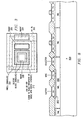
- Figure 3 is a top or plan view of the npn bipolar transistor layout described above.
- the structure is shown exclusive of the metal layers 254 and 256 and is included here to show the spatial relationship of the various mask levels used in the embodiment processes.
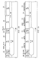
- the outer bounds of the buried layer are indicated by the dashed line 300 in Figure 3 and corresponds to element 202 in the series of cross-sections of Figures 2a to 21.
- the n-well 208 in Figure 2 is shown as the annulus 302 in Figure 3.
- the outer bounds of the collector contact n-moat 234 is shown as element 304 in Figure 3.
- the outer bounds of the base contact p-moat 242 is shown as element 306 in Figure 3.
- the outer bounds of the emitter contact n-moat 236 is shown in Figure 3 as element 308.
- the silicidation mask oxide 244 of Figure 2 is shown as the annulus 310 in Figure 3.
- the outer bounds of the mask that may be used for threshold adjustment implants in the emitter region, described hereinbelow in additional embodiments, is shown as element 312 in Figure 3.
- the masking of the VTN implants described in step (g) above and in Figure 2e is modified.
- the photoresist mask 422 is modified to cover the emitter region 400 in addition to the n-wells 408 covered in the first embodiment process described above.
- the portion of the p-well 412 beneath the emitter contact 436 is devoid of dopants from the VTN implants, in contrast to the substantially uniform lateral base doping of the first embodiment. Consequently, the base doping is set solely by the p-well 412 doping level, resulting in a bipolar transistor with higher gain (h fe ) than in the first embodiment process.
- the second preferred embodiment process is achieved with only a modification of an implant mask.
- An integrated circuit die that includes both types of bipolar transistor is therefore easily fabricated.
- Such an integrated circuit could therefore include a high H fe bandgap reference device (formed with the no-VTN implant npn transistor) as well as a higher Early voltage transistor (formed with the VTN implant npn transistor) as may be used in the output stage of an amplifier, for example.
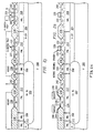
- Figure 5a is a spreading resistance plot of a transistor fabricated in accordance with the first preferred embodiment process, which includes the base VTN implants
- Figure 5b is a result of a transistor fabricated in accordance with the second preferred embodiment process, which omits the VTN implants. A comparison of the two plots makes clear the effect of the threshold adjustment, punch-through, and channel stop implants.
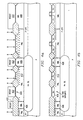
- the first and second preferred embodiment processes are modified as shown in Figures 6a and 6b.
- the mask used for the VTP implants described in step (h) above and in Figure 2f is modified to expose the emitter region 600 in addition to the n-wells 608.
- This modification involves the mask for the VTP implants, and hence may be used in conjunction with the second preferred embodiment process in which the modification involves the masking for the VTN implants.
- the third preferred embodiment could also be applied to the first preferred embodiment process.
- Figures 6a and 6b show the effects of the third preferred embodiment process on a structure that has been subjected to the second preferred embodiment process.
- the emitter region 600 is devoid of dopants from the VTN implants.
- the VTP implant results in an n-type region that extends deeper into the p-well 612 than the emitter 636 (shown in Figure 6b).
- the bipolar transistor produced by the third preferred embodiment process has a higher gain than that produced by the second preferred embodiment process.
- a fourth preferred embodiment in accordance with the invention is shown in Figures 7a and 7b.
- the bipolar transistor is formed in an n-well 700, rather than the p-well used in the first three embodiments described above.
- the base region 702 is formed with the VTN implants.
- the VTN implants counterdope the surface of n-well 700 to form the shallow (in the range of approximately 0.1 to 0.2 um) base region.
- the shallow base width makes possible an npn transistor capable of higher operating speeds than the thicker-base embodiments described above where the base depth is set by the epi layer thickness.
- the use of a single set of implants for both the VTN implants and the base of the npn transistor saves a mask and the associated costs incurred in prior art approaches in which two different implant steps are used for the npn base and the threshold adjustment, channel-stop, and punch-through prevention implants of the n-channel MOS transistor.
- the emitter region 704 and base contact 706 are formed in the base region 702 as in the embodiments described above.
- the collector contact 708 is formed in n-well 700, which acts as the collector for the transistor. This process relies on modified masks for the n-well and VTN implants, but otherwise adds no complexity to the embodiment processes described above.
- the fourth preferred embodiment structure can also be arranged to occupy less die space than the first preferred embodiment structure, for example.
- the annular n-well 302 (element 208 in Figures 2a to 21) used for isolating the base region 211 from the remainder of epi layer 211 in Figure 21 can be avoided with the implanted base approach of the fourth preferred embodiment structure, thus saving die space.
- FIG. 8 A fifth preferred embodiment in accordance with the invention is shown in Figure 8.
- the structure of Figure 8 is similar to that of Figure 7b, except the buried layer 710 is omitted in Figure 8.
- the structure of Figure 8 provides an isolated vertical npn transistor that is manufacturable in standard CMOS processes, which typically lack the process steps involved in forming buried layers.
Landscapes
- Metal-Oxide And Bipolar Metal-Oxide Semiconductor Integrated Circuits (AREA)
- Bipolar Integrated Circuits (AREA)
- Bipolar Transistors (AREA)
- Element Separation (AREA)
Applications Claiming Priority (2)
| Application Number | Priority Date | Filing Date | Title |
|---|---|---|---|
| US79444 | 1987-07-30 | ||
| US7944498P | 1998-03-26 | 1998-03-26 |
Publications (1)
| Publication Number | Publication Date |
|---|---|
| EP0948046A1 true EP0948046A1 (fr) | 1999-10-06 |
Family
ID=22150598
Family Applications (1)
| Application Number | Title | Priority Date | Filing Date |
|---|---|---|---|
| EP99200902A Withdrawn EP0948046A1 (fr) | 1998-03-26 | 1999-03-25 | Dispositif bipolaire et CMOS fusionné et procédé |
Country Status (3)
| Country | Link |
|---|---|
| US (1) | US6352887B1 (fr) |
| EP (1) | EP0948046A1 (fr) |
| JP (2) | JPH11312746A (fr) |
Cited By (3)
| Publication number | Priority date | Publication date | Assignee | Title |
|---|---|---|---|---|
| US6803634B2 (en) | 2001-11-07 | 2004-10-12 | Denso Corporation | Stabilization in device characteristics of a bipolar transistor that is included in a semiconductor device with a CMOSFET |
| WO2008100312A1 (fr) * | 2007-02-14 | 2008-08-21 | Agere Systems, Inc. | Procédé de réduction de la résistance de collecteur d'un transistor bipolaire et intégration dans un flux cmos |
| EP2317541A3 (fr) * | 2009-10-22 | 2014-05-07 | Sanyo Electric Co., Ltd. | Procédé de fabrication d'un dispositif semi-conducteur |
Families Citing this family (20)
| Publication number | Priority date | Publication date | Assignee | Title |
|---|---|---|---|---|
| JP2001274257A (ja) * | 2000-03-27 | 2001-10-05 | Mitsubishi Electric Corp | 半導体装置およびその製造方法 |
| JP2003197908A (ja) * | 2001-09-12 | 2003-07-11 | Seiko Instruments Inc | 半導体素子及びその製造方法 |
| US6521487B1 (en) * | 2001-12-05 | 2003-02-18 | United Microelectronics Corp. | Method for making a thyristor |
| US7019377B2 (en) * | 2002-12-17 | 2006-03-28 | Micrel, Inc. | Integrated circuit including high voltage devices and low voltage devices |
| US6861303B2 (en) * | 2003-05-09 | 2005-03-01 | Texas Instruments Incorporated | JFET structure for integrated circuit and fabrication method |
| US7282771B2 (en) * | 2005-01-25 | 2007-10-16 | International Business Machines Corporation | Structure and method for latchup suppression |
| US7875513B2 (en) * | 2006-04-26 | 2011-01-25 | Fabio Pellizzer | Self-aligned bipolar junction transistors |
| US20090026578A1 (en) * | 2007-07-27 | 2009-01-29 | Micrel, Inc. | Vertical NPN Transistor Fabricated in a CMOS Process With Improved Electrical Characteristics |
| KR20090068084A (ko) * | 2007-12-22 | 2009-06-25 | 주식회사 동부하이텍 | 반도체 소자 및 그 제조 방법 |
| US8035196B2 (en) * | 2008-04-02 | 2011-10-11 | Zarlink Semiconductor (Us) Inc. | Methods of counter-doping collector regions in bipolar transistors |
| JP5423151B2 (ja) * | 2009-05-28 | 2014-02-19 | 富士通セミコンダクター株式会社 | 半導体装置とその製造方法 |
| JP5469439B2 (ja) * | 2009-11-20 | 2014-04-16 | ルネサスエレクトロニクス株式会社 | 半導体装置およびその製造方法 |
| JP2010109379A (ja) * | 2009-12-25 | 2010-05-13 | Mitsumi Electric Co Ltd | Cmosデバイスの製造方法 |
| US20130071994A1 (en) * | 2011-09-20 | 2013-03-21 | Alpha And Omega Semiconductor Incorporated | Method of integrating high voltage devices |
| US20130069157A1 (en) * | 2011-09-20 | 2013-03-21 | Alpha And Omega Semiconductor Incorporated | Semiconductor chip integrating high and low voltage devices |
| US9214457B2 (en) | 2011-09-20 | 2015-12-15 | Alpha & Omega Semiconductor Incorporated | Method of integrating high voltage devices |
| CN103515324B (zh) * | 2012-06-30 | 2016-10-26 | 万国半导体股份有限公司 | 集成高压器件的方法 |
| KR20160004069A (ko) * | 2014-07-02 | 2016-01-12 | 에스케이하이닉스 주식회사 | 반도체 장치 및 그 제조 방법 |
| JP2016157730A (ja) * | 2015-02-23 | 2016-09-01 | 旭化成エレクトロニクス株式会社 | 半導体装置の製造方法及び半導体装置 |
| CN111696854B (zh) * | 2019-03-13 | 2022-09-09 | 无锡华润上华科技有限公司 | 半导体器件的制造方法 |
Citations (4)
| Publication number | Priority date | Publication date | Assignee | Title |
|---|---|---|---|---|
| JPS63175463A (ja) * | 1987-01-14 | 1988-07-19 | Nec Corp | バイmos集積回路の製造方法 |
| EP0398247A2 (fr) * | 1989-05-17 | 1990-11-22 | Kabushiki Kaisha Toshiba | Dispositif semi-conducteur et son procédé de fabrication |
| EP0613181A1 (fr) * | 1993-02-26 | 1994-08-31 | STMicroelectronics S.r.l. | Transistor bipolaire compatible avec la technologie CMOS |
| EP0843355A1 (fr) * | 1996-11-19 | 1998-05-20 | STMicroelectronics S.A. | Fabrication de circuits intégrés bipolaires/CMOS et d'un condensateur |
Family Cites Families (28)
| Publication number | Priority date | Publication date | Assignee | Title |
|---|---|---|---|---|
| NL8103031A (nl) * | 1980-08-04 | 1982-03-01 | Fairchild Camera Instr Co | Werkwijze voor het vervaardigen van een geintegreerde logische injectiecel met zelfgecentreerde collector en basis en gereduceerde basisweerstand en cel vervaardigd volgens deze werkwijze. |
| JPS57136358A (en) * | 1981-02-17 | 1982-08-23 | Seiko Instr & Electronics Ltd | Integrated circuit device and manufacture thereof |
| JPS57198650A (en) * | 1981-06-01 | 1982-12-06 | Toshiba Corp | Semiconductor device and manufacture therefor |
| JPS58165368A (ja) * | 1982-03-26 | 1983-09-30 | Hitachi Ltd | 半導体装置の製造法 |
| US4536945A (en) * | 1983-11-02 | 1985-08-27 | National Semiconductor Corporation | Process for producing CMOS structures with Schottky bipolar transistors |
| JPS61245563A (ja) * | 1985-04-24 | 1986-10-31 | Hitachi Ltd | バイポ−ラcmos半導体装置 |
| US5023193A (en) * | 1986-07-16 | 1991-06-11 | National Semiconductor Corp. | Method for simultaneously fabricating bipolar and complementary field effect transistors using a minimal number of masks |
| US4994887A (en) * | 1987-11-13 | 1991-02-19 | Texas Instruments Incorporated | High voltage merged bipolar/CMOS technology |
| JP2553600B2 (ja) * | 1987-12-11 | 1996-11-13 | 松下電子工業株式会社 | BiMOS半導体集積回路 |
| JPH02260641A (ja) * | 1989-03-31 | 1990-10-23 | Toshiba Corp | 半導体集積回路 |
| US5171702A (en) * | 1989-07-21 | 1992-12-15 | Texas Instruments Incorporated | Method for forming a thick base oxide in a BiCMOS process |
| JPH04214664A (ja) * | 1990-12-12 | 1992-08-05 | Toshiba Corp | 半導体装置 |
| JPH05267331A (ja) * | 1992-03-21 | 1993-10-15 | Ricoh Co Ltd | Mos型半導体装置の製造方法 |
| US5342794A (en) * | 1992-09-10 | 1994-08-30 | Vlsi Technology, Inc. | Method for forming laterally graded deposit-type emitter for bipolar transistor |
| US5407841A (en) * | 1992-10-30 | 1995-04-18 | Hughes Aircraft Company | CBiCMOS fabrication method using sacrificial gate poly |
| JP3343968B2 (ja) * | 1992-12-14 | 2002-11-11 | ソニー株式会社 | バイポーラ型半導体装置およびその製造方法 |
| US5422290A (en) * | 1994-02-28 | 1995-06-06 | National Semiconductor Corporation | Method of fabricating BiCMOS structures |
| JPH07307467A (ja) * | 1994-05-13 | 1995-11-21 | Fujitsu Ltd | 半導体装置及びその製造方法 |
| JPH08204040A (ja) * | 1995-01-25 | 1996-08-09 | Toshiba Corp | 半導体装置の製造方法 |
| JPH09260511A (ja) * | 1996-01-16 | 1997-10-03 | Mitsubishi Electric Corp | 半導体装置およびその製造方法 |
| US6245604B1 (en) * | 1996-01-16 | 2001-06-12 | Micron Technology | Bipolar-CMOS (BiCMOS) process for fabricating integrated circuits |
| US5843814A (en) * | 1996-02-15 | 1998-12-01 | Micron Technology, Inc. | Method of forming BiCMOS circuitry |
| KR100190029B1 (ko) * | 1996-03-19 | 1999-06-01 | 윤종용 | 바이씨모스 에스램 소자의 제조방법 |
| JPH1098120A (ja) * | 1996-09-19 | 1998-04-14 | Mitsubishi Electric Corp | 半導体装置およびその製造方法 |
| FR2756100B1 (fr) * | 1996-11-19 | 1999-02-12 | Sgs Thomson Microelectronics | Transistor bipolaire a emetteur inhomogene dans un circuit integre bicmos |
| FR2756104B1 (fr) * | 1996-11-19 | 1999-01-29 | Sgs Thomson Microelectronics | Fabrication de circuits integres bipolaires/cmos |
| US5945726A (en) * | 1996-12-16 | 1999-08-31 | Micron Technology, Inc. | Lateral bipolar transistor |
| JP4397061B2 (ja) * | 1998-09-03 | 2010-01-13 | 株式会社ルネサステクノロジ | 半導体装置の製造方法 |
-
1999
- 1999-03-25 US US09/276,780 patent/US6352887B1/en not_active Expired - Lifetime
- 1999-03-25 EP EP99200902A patent/EP0948046A1/fr not_active Withdrawn
- 1999-03-26 JP JP11084394A patent/JPH11312746A/ja active Pending
-
2008
- 2008-08-21 JP JP2008212623A patent/JP5089529B2/ja not_active Expired - Lifetime
Patent Citations (4)
| Publication number | Priority date | Publication date | Assignee | Title |
|---|---|---|---|---|
| JPS63175463A (ja) * | 1987-01-14 | 1988-07-19 | Nec Corp | バイmos集積回路の製造方法 |
| EP0398247A2 (fr) * | 1989-05-17 | 1990-11-22 | Kabushiki Kaisha Toshiba | Dispositif semi-conducteur et son procédé de fabrication |
| EP0613181A1 (fr) * | 1993-02-26 | 1994-08-31 | STMicroelectronics S.r.l. | Transistor bipolaire compatible avec la technologie CMOS |
| EP0843355A1 (fr) * | 1996-11-19 | 1998-05-20 | STMicroelectronics S.A. | Fabrication de circuits intégrés bipolaires/CMOS et d'un condensateur |
Non-Patent Citations (1)
| Title |
|---|
| PATENT ABSTRACTS OF JAPAN vol. 012, no. 447 (E - 685) 24 November 1988 (1988-11-24) * |
Cited By (4)
| Publication number | Priority date | Publication date | Assignee | Title |
|---|---|---|---|---|
| US6803634B2 (en) | 2001-11-07 | 2004-10-12 | Denso Corporation | Stabilization in device characteristics of a bipolar transistor that is included in a semiconductor device with a CMOSFET |
| WO2008100312A1 (fr) * | 2007-02-14 | 2008-08-21 | Agere Systems, Inc. | Procédé de réduction de la résistance de collecteur d'un transistor bipolaire et intégration dans un flux cmos |
| US7923340B2 (en) | 2007-02-14 | 2011-04-12 | Agere Systems Inc. | Method to reduce collector resistance of a bipolar transistor and integration into a standard CMOS flow |
| EP2317541A3 (fr) * | 2009-10-22 | 2014-05-07 | Sanyo Electric Co., Ltd. | Procédé de fabrication d'un dispositif semi-conducteur |
Also Published As
| Publication number | Publication date |
|---|---|
| JPH11312746A (ja) | 1999-11-09 |
| US6352887B1 (en) | 2002-03-05 |
| JP5089529B2 (ja) | 2012-12-05 |
| JP2009016856A (ja) | 2009-01-22 |
Similar Documents
| Publication | Publication Date | Title |
|---|---|---|
| US6352887B1 (en) | Merged bipolar and CMOS circuit and method | |
| US5169794A (en) | Method of fabrication of pnp structure in a common substrate containing npn or MOS structures | |
| US5171699A (en) | Vertical DMOS transistor structure built in an N-well CMOS-based BiCMOS process and method of fabrication | |
| EP1543546B1 (fr) | Procede d'fabrication d'un transistor a effet de champ isole dans un substrat depourvu de couche epitaxiale | |
| US5424572A (en) | Spacer formation in a semiconductor structure | |
| US8603873B2 (en) | High-gain bipolar junction transistor compatible with complementary metal-oxide-semiconductor (CMOS) process and method for fabricating the same | |
| US4694562A (en) | Method for manufacturing a semiconductor integrated device including bipolar and CMOS transistors | |
| US20100055860A1 (en) | Semiconductor Process and Integrated Circuit | |
| US6949424B2 (en) | Single poly-emitter PNP using DWELL diffusion in a BiCMOS technology | |
| US6861303B2 (en) | JFET structure for integrated circuit and fabrication method | |
| US20030073269A1 (en) | Low voltage high performance semiconductor devices and methods | |
| US5001073A (en) | Method for making bipolar/CMOS IC with isolated vertical PNP | |
| US5268312A (en) | Method of forming isolated wells in the fabrication of BiCMOS devices | |
| US7812403B2 (en) | Isolation structures for integrated circuit devices | |
| US8217426B2 (en) | Bipolar transistors with resistors | |
| US6071763A (en) | Method of fabricating layered integrated circuit | |
| US6297119B1 (en) | Semiconductor device and its manufacture | |
| US5010034A (en) | CMOS and bipolar fabrication process using selective epitaxial growth scalable to below 0.5 micron | |
| US6011283A (en) | Pillar emitter for BiCMOS devices | |
| US6797577B2 (en) | One mask PNP (or NPN) transistor allowing high performance | |
| US5972766A (en) | Method of manufacturing a bipolar transistor by using only two mask layers | |
| US6469362B2 (en) | High-gain pnp bipolar junction transistor in a CMOS device and method for forming the same | |
| US6548337B2 (en) | Method of manufacturing a high gain bipolar junction transistor with counterdoped base in CMOS technology | |
| US5604359A (en) | Parasitic PNP transistor with crystal defect layer in the emitter region | |
| JP3013784B2 (ja) | BiCMOS集積回路の製造方法 |
Legal Events
| Date | Code | Title | Description |
|---|---|---|---|
| PUAI | Public reference made under article 153(3) epc to a published international application that has entered the european phase |
Free format text: ORIGINAL CODE: 0009012 |
|
| AK | Designated contracting states |
Kind code of ref document: A1 Designated state(s): DE FR GB IT NL |
|
| AX | Request for extension of the european patent |
Free format text: AL;LT;LV;MK;RO;SI |
|
| 17P | Request for examination filed |
Effective date: 20000406 |
|
| AKX | Designation fees paid |
Free format text: DE FR GB IT NL |
|
| STAA | Information on the status of an ep patent application or granted ep patent |
Free format text: STATUS: THE APPLICATION IS DEEMED TO BE WITHDRAWN |
|
| 18D | Application deemed to be withdrawn |
Effective date: 20060613 |