EP0949715A2 - Contact amélioré pour un accouplement de signaux électriques résistant aux erreurs - Google Patents
Contact amélioré pour un accouplement de signaux électriques résistant aux erreurs Download PDFInfo
- Publication number
- EP0949715A2 EP0949715A2 EP99301873A EP99301873A EP0949715A2 EP 0949715 A2 EP0949715 A2 EP 0949715A2 EP 99301873 A EP99301873 A EP 99301873A EP 99301873 A EP99301873 A EP 99301873A EP 0949715 A2 EP0949715 A2 EP 0949715A2
- Authority
- EP
- European Patent Office
- Prior art keywords
- surface portion
- contact
- plug
- receptacle
- leading
- Prior art date
- Legal status (The legal status is an assumption and is not a legal conclusion. Google has not performed a legal analysis and makes no representation as to the accuracy of the status listed.)
- Granted
Links
Images


Classifications
-
- H—ELECTRICITY
- H05—ELECTRIC TECHNIQUES NOT OTHERWISE PROVIDED FOR
- H05K—PRINTED CIRCUITS; CASINGS OR CONSTRUCTIONAL DETAILS OF ELECTRIC APPARATUS; MANUFACTURE OF ASSEMBLAGES OF ELECTRICAL COMPONENTS
- H05K1/00—Printed circuits
- H05K1/02—Details
- H05K1/11—Printed elements for providing electric connections to or between printed circuits
- H05K1/117—Pads along the edge of rigid circuit boards, e.g. for pluggable connectors
-
- H—ELECTRICITY
- H01—ELECTRIC ELEMENTS
- H01R—ELECTRICALLY-CONDUCTIVE CONNECTIONS; STRUCTURAL ASSOCIATIONS OF A PLURALITY OF MUTUALLY-INSULATED ELECTRICAL CONNECTING ELEMENTS; COUPLING DEVICES; CURRENT COLLECTORS
- H01R13/00—Details of coupling devices of the kinds covered by groups H01R12/70 or H01R24/00 - H01R33/00
- H01R13/02—Contact members
- H01R13/03—Contact members characterised by the material, e.g. plating, or coating materials
-
- H—ELECTRICITY
- H01—ELECTRIC ELEMENTS
- H01R—ELECTRICALLY-CONDUCTIVE CONNECTIONS; STRUCTURAL ASSOCIATIONS OF A PLURALITY OF MUTUALLY-INSULATED ELECTRICAL CONNECTING ELEMENTS; COUPLING DEVICES; CURRENT COLLECTORS
- H01R13/00—Details of coupling devices of the kinds covered by groups H01R12/70 or H01R24/00 - H01R33/00
- H01R13/66—Structural association with built-in electrical component
- H01R13/665—Structural association with built-in electrical component with built-in electronic circuit
- H01R13/6666—Structural association with built-in electrical component with built-in electronic circuit with built-in overvoltage protection
-
- H—ELECTRICITY
- H01—ELECTRIC ELEMENTS
- H01R—ELECTRICALLY-CONDUCTIVE CONNECTIONS; STRUCTURAL ASSOCIATIONS OF A PLURALITY OF MUTUALLY-INSULATED ELECTRICAL CONNECTING ELEMENTS; COUPLING DEVICES; CURRENT COLLECTORS
- H01R2107/00—Four or more poles
-
- H—ELECTRICITY
- H01—ELECTRIC ELEMENTS
- H01R—ELECTRICALLY-CONDUCTIVE CONNECTIONS; STRUCTURAL ASSOCIATIONS OF A PLURALITY OF MUTUALLY-INSULATED ELECTRICAL CONNECTING ELEMENTS; COUPLING DEVICES; CURRENT COLLECTORS
- H01R2201/00—Connectors or connections adapted for particular applications
- H01R2201/20—Connectors or connections adapted for particular applications for testing or measuring purposes
-
- H—ELECTRICITY
- H01—ELECTRIC ELEMENTS
- H01R—ELECTRICALLY-CONDUCTIVE CONNECTIONS; STRUCTURAL ASSOCIATIONS OF A PLURALITY OF MUTUALLY-INSULATED ELECTRICAL CONNECTING ELEMENTS; COUPLING DEVICES; CURRENT COLLECTORS
- H01R24/00—Two-part coupling devices, or either of their cooperating parts, characterised by their overall structure
- H01R24/60—Contacts spaced along planar side wall transverse to longitudinal axis of engagement
-
- H—ELECTRICITY
- H05—ELECTRIC TECHNIQUES NOT OTHERWISE PROVIDED FOR
- H05K—PRINTED CIRCUITS; CASINGS OR CONSTRUCTIONAL DETAILS OF ELECTRIC APPARATUS; MANUFACTURE OF ASSEMBLAGES OF ELECTRICAL COMPONENTS
- H05K1/00—Printed circuits
- H05K1/16—Printed circuits incorporating printed electric components, e.g. printed resistors, capacitors or inductors
- H05K1/167—Printed circuits incorporating printed electric components, e.g. printed resistors, capacitors or inductors incorporating printed resistors
-
- H—ELECTRICITY
- H05—ELECTRIC TECHNIQUES NOT OTHERWISE PROVIDED FOR
- H05K—PRINTED CIRCUITS; CASINGS OR CONSTRUCTIONAL DETAILS OF ELECTRIC APPARATUS; MANUFACTURE OF ASSEMBLAGES OF ELECTRICAL COMPONENTS
- H05K2201/00—Indexing scheme relating to printed circuits covered by H05K1/00
- H05K2201/03—Conductive materials
- H05K2201/0332—Structure of the conductor
- H05K2201/0335—Layered conductors or foils
- H05K2201/0338—Layered conductor, e.g. layered metal substrate, layered finish layer or layered thin film adhesion layer
-
- Y—GENERAL TAGGING OF NEW TECHNOLOGICAL DEVELOPMENTS; GENERAL TAGGING OF CROSS-SECTIONAL TECHNOLOGIES SPANNING OVER SEVERAL SECTIONS OF THE IPC; TECHNICAL SUBJECTS COVERED BY FORMER USPC CROSS-REFERENCE ART COLLECTIONS [XRACs] AND DIGESTS
- Y10—TECHNICAL SUBJECTS COVERED BY FORMER USPC
- Y10S—TECHNICAL SUBJECTS COVERED BY FORMER USPC CROSS-REFERENCE ART COLLECTIONS [XRACs] AND DIGESTS
- Y10S439/00—Electrical connectors
- Y10S439/931—Conductive coating
-
- Y—GENERAL TAGGING OF NEW TECHNOLOGICAL DEVELOPMENTS; GENERAL TAGGING OF CROSS-SECTIONAL TECHNOLOGIES SPANNING OVER SEVERAL SECTIONS OF THE IPC; TECHNICAL SUBJECTS COVERED BY FORMER USPC CROSS-REFERENCE ART COLLECTIONS [XRACs] AND DIGESTS
- Y10—TECHNICAL SUBJECTS COVERED BY FORMER USPC
- Y10S—TECHNICAL SUBJECTS COVERED BY FORMER USPC CROSS-REFERENCE ART COLLECTIONS [XRACs] AND DIGESTS
- Y10S439/00—Electrical connectors
- Y10S439/951—PCB having detailed leading edge
Definitions
- This invention relates generally to electrical connectors for electronic devices. More particularly, the invention relates to electrical contacts for use in electrical connectors to prevent the generation of spurious signals upon mating of the connector.
- a recurrent problem with many prior art connectors is the generation of spurious signals upon mating of a peripheral electronic device to an electronic system which is already energized.
- the connector may induce a voltage pulse into the energized electronic system.
- the voltage pulse may travel through the electronic system, thereby introducing spurious errors into the system. This problem is known in the art as the "hot plug" problem.
- a connector assembly disclosed in U.S. Patent No. 4,747,783 attempts to eliminate timing and control circuitry for power applications.
- This connector assembly uses a long pin in the "plug” to first make contact with its mating "socket” to gradually increase the voltage to the socket until the entire plug makes mating contact with the socket.
- the plug comprises a pin having a thin insulating material covering the surface and a thin low resistive material covering the insulating material. When the plug makes initial contact with the socket, the current must pass through the resistive portion of the plug. This permits the electronic components in the peripheral device to charge gradually and eliminates the current surges which may result.
- This device is undesirable for several reasons. First, it requires the use of several contacts of differing lengths, thereby raising manual dexterity problems. Secondly, although the low resistance (i.e. 2-60 ohms) is sufficient to eliminate current surges in power transmissions, it is not sufficient to eliminate the voltage pulse from being introduced into the electronic system. In addition, the thin layer of low resistive material surrounding the thin layer of insulating material introduces an additional problem into the connection between the peripheral device and the electronic system; short capacitance. As explained previously, capacitance is undesirable in a connector.
- the present invention provides a plug contact having a high resistive portion within a plug for use in a signal connector assembly.
- the high resistive portion of the plug contact prevents a voltage spike.
- resistive portions with resistances ranging from 10k ⁇ to 1G ⁇ are necessary depending upon the application.
- the energy flow is gradually increased.
- the receptacle contacts within the receptacle pass the high resistive portion and make contact with the conductive portion of the plug contact, thereby permitting transmission of valid signals without the generation of spurious errors.
- the receptacle contact, or both the plug contact and the receptacle contact may have the high resistive portion.
- the preferred embodiment of the connector assembly of the present invention comprises a plug 6 for mating with a corresponding receptacle 8 .
- a plug 6 for mating with a corresponding receptacle 8 .
- plug contact 7 is typically at least two or more plug contacts 7 within every plug 6 for mating with corresponding receptacle contacts 15 .
- the shape of the plug 6 is not central to the present invention.
- the plug 6 and plug contact 7 are illustrated as rectangular, although those of skill in the art will realize that many other shapes could be used without departing from the spirit of the present invention.
- the plug contact 7 comprises a conductive portion 14 which can be made from any conductive material, (such as brass, nickel, gold, copper or a superconductor, etc.) and a highly resistive portion 12 .
- the resistive portion 12 is generally rectangular shaped and extends across the width W of the plug contact 7 .
- the resistive portion 12 comprises a layer of highly resistive material inset into the surface 16 of the plug 6 , with a first end 11 of the resistive portion 12 exposed to the receptacle 8 and a second end 13 of the resistive portion 12 in contact with the conductive portion 14 .
- a typical receptacle 8 includes a receptacle contact 15 for each corresponding plug contact 7 which electrically mates with its corresponding receptacle contact 15 as the plug 6 of the peripheral device (not shown) is inserted into receptacle 8 of the electronic system (not shown).
- the first end of the plug 6 is inserted into the cavity of the receptacle 8 .
- the receptacle contact 15 will make first contact with the resistive portion 12 . Since it is contemplated that the electronic system will be energized, this will permit energy from the electronic system to begin flowing from the receptacle contact 15 , through the resistive portion 12 and into the conductive portion 14 of the plug contact 7 .
- the resistive portion 12 reduces the magnitude voltage pulses such that they will not present errors into the electronic system, as will be explained in detail hereinafter. A portion of the voltage "seen" by the plug 6 will drop across the resistive portion 12 .
- the receptacle contact 15 passes along the surface 16 of the resistive portion 12 until it finally reaches the conductive portion 14 of the plug contact 7 .
- the receptacle contact 15 will be in direct contact with the conductive portion 14 of the plug contact 7 . Accordingly, there will be no voltage drop across the resistive portion 12 of the plug contact 7 .
- the arrangement of the present invention specifically limits the capacitance between the metallic portions of the plug and receptacle contacts 7 , 15 , (it bypasses the high resistance), to an acceptably low level. It does this by minimizing their effective coupling area and the effective dielectric constant between them, which is primarily air.
- a primary aspect of preventing a voltage pulse is to reduce the initial voltage seen by plug contact 7 upon insertion of the plug 6 into the receptacle 8 .
- the resistive portion 12 reduces the initial voltage seen by the receptacle contact 15 .
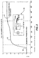
- the graph represents the voltage seen by the receptacle contact 15 as the plug 6 is removed from the receptacle 8 . Referring to the portion of the graph to the left of point 92 , this shows a short circuit voltage of 0V across the plug contact 7 while the plug contact 7 is in full contact with the receptacle contact 15 . At point 92 , the receptacle contact 15 contacts the resistive portion 12 .
- the resistive portion 12 permits the voltage as seen across the receptacle contact 15 , to increase gradually along the sloped (or curved) portion 93 of the graph as the plug 6 is removed from the receptacle 8 .
- the receptacle contact 15 no longer contacts the plug contact 7 . Accordingly, 5V is seen by the receptacle contact 15 .
- Curve 93 shows the gradual transition between points 91 and 92 which prevents voltage pulses which will prevent the introduction of errors into the system.
- the graph would be reversed upon insertion of a plug 6 into a receptacle 8 .
- the high resistance of resistive portion 12 limits the rate of flow of current from the system bus to the "cold" device being hot-plugged into the system.
- the evidence of too fast a current transfer is a transient voltage pulse at the connection to the operating system.
- the transient voltage pulse decays as it propagates along the system bus, primarily because the bus and other attached devices are sources of charge. Accordingly, the high resistance slows the charge transfer enough to provide time for the charge to be adequately replaced. If the voltage cannot dip below the sensing threshold of an adjacent device, an error cannot occur.
- Figure 3 is a graph of the electrical resistance as measured from the end of the plug contact 7 .
- This graph is based on a resistive portion 12 of a rectangular shape 0.33mm (13 mils) wide and 0.38mm (15 mils) long.
- the high resistive material had a resistivity of 2.29 x 10 9 ohm.metres (9 x 10 10 ohm.inches).
- the resistance increases as the thickness of the resistive portion 12 increases.
- curve 20 when a resistive portion thickness of 0.20 mm (8 mils) is used, a resistance of 10M ⁇ is achieved at the first end 11 of the plug contact 7 , which gradually decreases until the second end 13 is reached where the resistance is nominally Zero.
- Curves 21 , 22 and 23 illustrate that the resistance decreases with a decrease in resistive portion thickness.
- the shape of the curves also differs as the resistive portion thickness is changed.
- the thickness of the resistive portion 12 was kept constant at 0.10mm (4 mils) while the resistivity of the resistive portion 12 was varied.
- Curve 31 illustrates a high resistivity of 4.57 x 10 9 ohm.metres (1.8 x 10 11 ohm. inches).
- the resistance measured at the first end 11 of the plug contact 7 is almost 16 megohms, which decreases gradually to zero at the second end 13 .
- Curves 32 and 33 illustrate that as the resistivity of the material is decreased, the resistance measured along the plug contact 7 will also decrease.
- the present invention can be adapted to different uses and applications. However, it is also extremely important to reduce the short capacitance to a negligible level.
- the short capacitance is reduced by keeping the thickness of the inlay 12 relatively thick, [i.e. in applying the present invention to a SCSI Bus, typically approximately 0.13 mm (5 mils)].
- connector assemblies can be created with desirable characteristics by preventing voltage surges for various types of signals and applications.
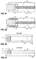
- the resistive portion 12 has a tapered profile.
- the resistive transition curves that result as the receptacle contact 15 passes over the resistive portion 12 can be varied as desired for a particular application.
- Figure 5b depicts an alternative embodiment with the resistive portion 12 in a stepwise-tapered profile 17 .
- the resistive transition curves can be varied as desired.
- a third alternative embodiment is shown in Figure 5c .
- the resistive portion 12 consists of two or more materials with varying resistivities.
- a fourth alternative embodiment shows, the resistive portion 12 extending from the conducting portion 14 .
- a conducting barb 18 extends from the conducting body 14 into the resistive portion 12 .
- a fifth alternative embodiment, Figure 5e has the resistive portion 12 extending into a hole 19 in the conducting portion 14 .
- Figure 5f depicts a sixth embodiment.
- the conductive body 14 is surrounded by a high resistive housing 30 .
- Receptacle contact 15 first makes contact with high resistive housing 30 .
- the receptacle contact sees essentially no resistance.
- the housing 30 is non-conductive. However, high resistive portions 12 make initial contact with receptacle contact 15 .
- the high resistive portions 12 are electrically connected and may be physically connected (not shown) to conducting portion 14 .
- Figures 5h and 5i depict a plug 7 having a housing 85 surrounding a first high resistance 31 portion and a second low resistance portion 32 . Upon full mating, the receptacle contact 15 is in full contact with the low resistance portion 32 .
- Figure 6 illustrates that the present instant invention may also be used with the contacts on a printed circuit board.
- the resistive portions 70A-N of the instant invention may be employed in one or more plug contacts 72A-N on a conventional printed circuit board 71.
- Figure 7 shows that the present invention may be adapted to various shaped applications. For instance, a plug 83 with a cylindrical shape with a resistive portion 81 and conductive portion 82 .
- Receptacle contacts 84 within the receptacle 85 make contact with the resistive portion 81 prior to the conductive portion 82 .
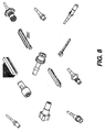
- Figure 8 illustrates some prior art electrical connectors.
- the size and shape of the connectors vary.
- the present invention can be used with the contacts within these various connectors.
Landscapes
- Engineering & Computer Science (AREA)
- Microelectronics & Electronic Packaging (AREA)
- Details Of Connecting Devices For Male And Female Coupling (AREA)
- Coupling Device And Connection With Printed Circuit (AREA)
Priority Applications (1)
| Application Number | Priority Date | Filing Date | Title |
|---|---|---|---|
| EP04104604A EP1489699A3 (fr) | 1998-03-13 | 1999-03-11 | Contact amélioré pour un accouplement de signaux électriques |
Applications Claiming Priority (2)
| Application Number | Priority Date | Filing Date | Title |
|---|---|---|---|
| US42400 | 1998-03-13 | ||
| US09/042,400 US6296499B1 (en) | 1998-03-13 | 1998-03-13 | Contact for error resistant coupling of electrical signals |
Related Child Applications (1)
| Application Number | Title | Priority Date | Filing Date |
|---|---|---|---|
| EP04104604A Division EP1489699A3 (fr) | 1998-03-13 | 1999-03-11 | Contact amélioré pour un accouplement de signaux électriques |
Publications (3)
| Publication Number | Publication Date |
|---|---|
| EP0949715A2 true EP0949715A2 (fr) | 1999-10-13 |
| EP0949715A3 EP0949715A3 (fr) | 2000-11-15 |
| EP0949715B1 EP0949715B1 (fr) | 2004-09-29 |
Family
ID=21921732
Family Applications (2)
| Application Number | Title | Priority Date | Filing Date |
|---|---|---|---|
| EP04104604A Withdrawn EP1489699A3 (fr) | 1998-03-13 | 1999-03-11 | Contact amélioré pour un accouplement de signaux électriques |
| EP99301873A Expired - Lifetime EP0949715B1 (fr) | 1998-03-13 | 1999-03-11 | Contact amélioré pour un accouplement de signaux électriques résistant aux erreurs |
Family Applications Before (1)
| Application Number | Title | Priority Date | Filing Date |
|---|---|---|---|
| EP04104604A Withdrawn EP1489699A3 (fr) | 1998-03-13 | 1999-03-11 | Contact amélioré pour un accouplement de signaux électriques |
Country Status (4)
| Country | Link |
|---|---|
| US (2) | US6296499B1 (fr) |
| EP (2) | EP1489699A3 (fr) |
| JP (1) | JP4345938B2 (fr) |
| DE (1) | DE69920561T2 (fr) |
Cited By (3)
| Publication number | Priority date | Publication date | Assignee | Title |
|---|---|---|---|---|
| WO2000054370A3 (fr) * | 1999-03-12 | 2001-02-15 | Whitaker Corp | Ensemble de connexion permettant le couplage de signaux electriques resistant aux erreurs |
| EP2705577A4 (fr) * | 2011-05-03 | 2015-01-07 | Cardioinsight Technologies Inc | Résistance à haute tension d'une interface de connecteur |
| KR20200026583A (ko) * | 2018-09-03 | 2020-03-11 | 삼성전자주식회사 | 입출력 단자 및 이를 포함하는 전자장치 |
Families Citing this family (11)
| Publication number | Priority date | Publication date | Assignee | Title |
|---|---|---|---|---|
| JP2001266985A (ja) * | 2000-03-24 | 2001-09-28 | Fujikura Ltd | オス型端子並びにこれを用いたコネクタ及び電気接続構造 |
| US6537092B2 (en) * | 2001-02-02 | 2003-03-25 | Autonetworks Technologies, Ltd | Arc discharge suppressive connector |
| US6857887B1 (en) * | 2003-10-29 | 2005-02-22 | Hewlett-Packard Development Company, L.P. | Current limit engagement apparatus |
| US7651382B2 (en) * | 2006-12-01 | 2010-01-26 | Interconnect Portfolio Llc | Electrical interconnection devices incorporating redundant contact points for reducing capacitive stubs and improved signal integrity |
| US7371091B2 (en) | 2006-06-22 | 2008-05-13 | Honeywell International, Inc. | Method and apparatus for integrated hot swap connector pins for AC and DC electric power systems |
| KR101719699B1 (ko) * | 2010-10-05 | 2017-03-27 | 삼성전자주식회사 | 메모리 모듈 및 이의 제조 방법 |
| WO2012151371A2 (fr) * | 2011-05-03 | 2012-11-08 | Cardioinsight Technologies, Inc. | Résistance à haute tension pour un connecteur fixé à une carte de circuit imprimé |
| CN104871654B (zh) * | 2012-12-18 | 2018-04-06 | 日本电气株式会社 | 电子基板及其接头连接的结构 |
| JP6631169B2 (ja) * | 2015-09-14 | 2020-01-15 | 株式会社オートネットワーク技術研究所 | 通電システム |
| CN108429028B (zh) | 2017-02-13 | 2023-05-30 | 泰连公司 | 抑制电谐振的电连接器 |
| US11394146B2 (en) * | 2020-04-07 | 2022-07-19 | Quanta Computer Inc. | Treated connection pins for high speed expansion sockets |
Family Cites Families (13)
| Publication number | Priority date | Publication date | Assignee | Title |
|---|---|---|---|---|
| US1770839A (en) | 1926-11-01 | 1930-07-15 | Gen Electric | Electric contact |
| US2716737A (en) | 1952-06-17 | 1955-08-30 | Garland A Maberry | Electric cable safety connectors |
| US4002496A (en) * | 1974-12-19 | 1977-01-11 | Japan Storage Battery Co., Ltd. | Catalytic device for storage battery |
| US4002396A (en) | 1976-02-13 | 1977-01-11 | Kearney-National, Inc. | Electric connector apparatus |
| US4079440A (en) | 1977-01-19 | 1978-03-14 | Hitachi, Ltd. | Printed circuit board capable of being inserted and withdrawn on on-line status |
| US4117291A (en) | 1977-05-19 | 1978-09-26 | Gte Automatic Electric Laboratories Incorporated | Reed switch |
| US4245270A (en) | 1978-12-26 | 1981-01-13 | Rockwell International Corporation | Circuit card with soft power switch |
| JPS6332881A (ja) | 1986-07-25 | 1988-02-12 | 日本テキサス・インスツルメンツ株式会社 | Icソケツト |
| US4747783A (en) | 1986-10-28 | 1988-05-31 | International Business Machines Corporation | Resistive pin for printed circuit card connector |
| US4897055A (en) * | 1988-11-28 | 1990-01-30 | International Business Machines Corp. | Sequential Connecting device |
| US5236789A (en) * | 1991-07-01 | 1993-08-17 | Olin Corporation | Palladium alloys having utility in electrical applications |
| US5213517A (en) | 1992-02-10 | 1993-05-25 | G & H Technology, Inc. | Separable electrodes with electric arc quenching means |
| US6102742A (en) * | 1998-06-30 | 2000-08-15 | Methode Electronics, Inc. | Electrical connector having variable resistance contacts |
-
1998
- 1998-03-13 US US09/042,400 patent/US6296499B1/en not_active Expired - Lifetime
-
1999
- 1999-03-11 EP EP04104604A patent/EP1489699A3/fr not_active Withdrawn
- 1999-03-11 EP EP99301873A patent/EP0949715B1/fr not_active Expired - Lifetime
- 1999-03-11 JP JP6505099A patent/JP4345938B2/ja not_active Expired - Fee Related
- 1999-03-11 DE DE69920561T patent/DE69920561T2/de not_active Expired - Lifetime
-
2001
- 2001-08-08 US US09/924,641 patent/US6802729B2/en not_active Expired - Lifetime
Cited By (6)
| Publication number | Priority date | Publication date | Assignee | Title |
|---|---|---|---|---|
| WO2000054370A3 (fr) * | 1999-03-12 | 2001-02-15 | Whitaker Corp | Ensemble de connexion permettant le couplage de signaux electriques resistant aux erreurs |
| EP2705577A4 (fr) * | 2011-05-03 | 2015-01-07 | Cardioinsight Technologies Inc | Résistance à haute tension d'une interface de connecteur |
| US9472879B2 (en) | 2011-05-03 | 2016-10-18 | Cardioinsight Technologies, Inc. | High-voltage resistance of a connector interface |
| KR20200026583A (ko) * | 2018-09-03 | 2020-03-11 | 삼성전자주식회사 | 입출력 단자 및 이를 포함하는 전자장치 |
| EP3832805A4 (fr) * | 2018-09-03 | 2021-09-29 | Samsung Electronics Co., Ltd. | Terminal d'entrée/sortie et dispositif électronique le comportant |
| US11552431B2 (en) | 2018-09-03 | 2023-01-10 | Samsung Electronics Co., Ltd. | Input/output terminal and electronic device comprising same |
Also Published As
| Publication number | Publication date |
|---|---|
| EP1489699A3 (fr) | 2004-12-29 |
| EP1489699A2 (fr) | 2004-12-22 |
| JPH11297391A (ja) | 1999-10-29 |
| US6802729B2 (en) | 2004-10-12 |
| DE69920561D1 (de) | 2004-11-04 |
| EP0949715B1 (fr) | 2004-09-29 |
| DE69920561T2 (de) | 2005-10-27 |
| US20030207627A1 (en) | 2003-11-06 |
| EP0949715A3 (fr) | 2000-11-15 |
| US6296499B1 (en) | 2001-10-02 |
| JP4345938B2 (ja) | 2009-10-14 |
Similar Documents
| Publication | Publication Date | Title |
|---|---|---|
| EP0265766B1 (fr) | Fiche de connecteur | |
| EP0949715B1 (fr) | Contact amélioré pour un accouplement de signaux électriques résistant aux erreurs | |
| US7102868B2 (en) | High voltage surge protection element for use with CATV coaxial cable connectors | |
| US11133623B2 (en) | Wet contact detection in external accessory connector | |
| US5290191A (en) | Interface conditioning insert wafer | |
| JP3587193B2 (ja) | 知的に識別可能なコネクタ | |
| KR970002781B1 (ko) | 멀티 드롭형 버스라인 시스템 | |
| EP0733274B1 (fr) | Raccord coaxial a regulation d'impedance | |
| CN1132274C (zh) | 适用于轴向定位的连接器组件 | |
| WO2006124969A2 (fr) | Connecteur electrique a ressort helicoidal biseaute integre | |
| JP2937385B2 (ja) | モジュール付コンピュータバス構造 | |
| US6310410B1 (en) | Method and apparatus for reducing source voltage deviation in hot plug applications | |
| US6790097B1 (en) | System and method for preventing cable discharge events | |
| US7682192B2 (en) | Electrical receptacle and circuit board with controlled skew | |
| JP4368015B2 (ja) | 棒状グロープラグ | |
| SE433990B (sv) | Overgangskontaktanordning avsedd for hopkoppling av tva olika koaxialkablar | |
| EP0717469A2 (fr) | Connecteur du type D-sub avec protection contre les surtensions | |
| US7126360B1 (en) | Differential signal acquisition probe having retractable double cushioned probing tips with EOS/ESD protection capabilities | |
| WO1998027625A1 (fr) | Adaptateur telephonique | |
| JP2639364B2 (ja) | コネクタ | |
| US6121777A (en) | Apparatus for detecting at least one property of a cable | |
| WO2000054370A2 (fr) | Ensemble de connexion permettant le couplage de signaux electriques resistant aux erreurs | |
| JPH07335329A (ja) | 突入電流制限接続器 | |
| JPH06243939A (ja) | プリント基板用コネクタの挿抜力・搭載力軽減法 | |
| CN119046072A (zh) | 终端以及插入检测系统 |
Legal Events
| Date | Code | Title | Description |
|---|---|---|---|
| PUAI | Public reference made under article 153(3) epc to a published international application that has entered the european phase |
Free format text: ORIGINAL CODE: 0009012 |
|
| AK | Designated contracting states |
Kind code of ref document: A2 Designated state(s): DE FR GB IE IT |
|
| AX | Request for extension of the european patent |
Free format text: AL;LT;LV;MK;RO;SI |
|
| PUAL | Search report despatched |
Free format text: ORIGINAL CODE: 0009013 |
|
| AK | Designated contracting states |
Kind code of ref document: A3 Designated state(s): AT BE CH CY DE DK ES FI FR GB GR IE IT LI LU MC NL PT SE |
|
| AX | Request for extension of the european patent |
Free format text: AL;LT;LV;MK;RO;SI |
|
| 17P | Request for examination filed |
Effective date: 20010514 |
|
| AKX | Designation fees paid |
Free format text: DE FR GB IE IT |
|
| GRAG | Despatch of communication of intention to grant |
Free format text: ORIGINAL CODE: EPIDOS AGRA |
|
| 17Q | First examination report despatched |
Effective date: 20011024 |
|
| GRAG | Despatch of communication of intention to grant |
Free format text: ORIGINAL CODE: EPIDOS AGRA |
|
| GRAP | Despatch of communication of intention to grant a patent |
Free format text: ORIGINAL CODE: EPIDOSNIGR1 |
|
| GRAS | Grant fee paid |
Free format text: ORIGINAL CODE: EPIDOSNIGR3 |
|
| GRAA | (expected) grant |
Free format text: ORIGINAL CODE: 0009210 |
|
| AK | Designated contracting states |
Kind code of ref document: B1 Designated state(s): DE FR GB IE IT |
|
| PG25 | Lapsed in a contracting state [announced via postgrant information from national office to epo] |
Ref country code: IT Free format text: LAPSE BECAUSE OF FAILURE TO SUBMIT A TRANSLATION OF THE DESCRIPTION OR TO PAY THE FEE WITHIN THE PRESCRIBED TIME-LIMIT;WARNING: LAPSES OF ITALIAN PATENTS WITH EFFECTIVE DATE BEFORE 2007 MAY HAVE OCCURRED AT ANY TIME BEFORE 2007. THE CORRECT EFFECTIVE DATE MAY BE DIFFERENT FROM THE ONE RECORDED. Effective date: 20040929 |
|
| REG | Reference to a national code |
Ref country code: GB Ref legal event code: FG4D |
|
| GRAI | Information related to approval/disapproval following communication of intention to grant deleted |
Free format text: ORIGINAL CODE: EPIDOSDAGR3 |
|
| GRAK | Information related to despatch of communication of intention to grant deleted |
Free format text: ORIGINAL CODE: EPIDOSDAGR1 |
|
| REG | Reference to a national code |
Ref country code: IE Ref legal event code: FG4D |
|
| REF | Corresponds to: |
Ref document number: 69920561 Country of ref document: DE Date of ref document: 20041104 Kind code of ref document: P |
|
| PG25 | Lapsed in a contracting state [announced via postgrant information from national office to epo] |
Ref country code: IE Free format text: LAPSE BECAUSE OF NON-PAYMENT OF DUE FEES Effective date: 20050311 |
|
| PLBE | No opposition filed within time limit |
Free format text: ORIGINAL CODE: 0009261 |
|
| STAA | Information on the status of an ep patent application or granted ep patent |
Free format text: STATUS: NO OPPOSITION FILED WITHIN TIME LIMIT |
|
| ET | Fr: translation filed | ||
| 26N | No opposition filed |
Effective date: 20050630 |
|
| REG | Reference to a national code |
Ref country code: IE Ref legal event code: MM4A |
|
| REG | Reference to a national code |
Ref country code: FR Ref legal event code: PLFP Year of fee payment: 18 |
|
| REG | Reference to a national code |
Ref country code: FR Ref legal event code: PLFP Year of fee payment: 19 |
|
| REG | Reference to a national code |
Ref country code: FR Ref legal event code: PLFP Year of fee payment: 20 |
|
| PGFP | Annual fee paid to national office [announced via postgrant information from national office to epo] |
Ref country code: GB Payment date: 20180307 Year of fee payment: 20 Ref country code: DE Payment date: 20180227 Year of fee payment: 20 |
|
| PGFP | Annual fee paid to national office [announced via postgrant information from national office to epo] |
Ref country code: FR Payment date: 20180223 Year of fee payment: 20 |
|
| REG | Reference to a national code |
Ref country code: DE Ref legal event code: R071 Ref document number: 69920561 Country of ref document: DE |
|
| REG | Reference to a national code |
Ref country code: GB Ref legal event code: PE20 Expiry date: 20190310 |
|
| PG25 | Lapsed in a contracting state [announced via postgrant information from national office to epo] |
Ref country code: GB Free format text: LAPSE BECAUSE OF EXPIRATION OF PROTECTION Effective date: 20190310 |