EP0952549B1 - Circuit de désactivation de la détection de transition de flanc pour changer des caractéristiques d'opération d'un dispositif de mémoire - Google Patents
Circuit de désactivation de la détection de transition de flanc pour changer des caractéristiques d'opération d'un dispositif de mémoire Download PDFInfo
- Publication number
- EP0952549B1 EP0952549B1 EP99300541A EP99300541A EP0952549B1 EP 0952549 B1 EP0952549 B1 EP 0952549B1 EP 99300541 A EP99300541 A EP 99300541A EP 99300541 A EP99300541 A EP 99300541A EP 0952549 B1 EP0952549 B1 EP 0952549B1
- Authority
- EP
- European Patent Office
- Prior art keywords
- signal
- address
- generating
- transition
- etd
- Prior art date
- Legal status (The legal status is an assumption and is not a legal conclusion. Google has not performed a legal analysis and makes no representation as to the accuracy of the status listed.)
- Expired - Lifetime
Links
Images


Classifications
-
- G—PHYSICS
- G11—INFORMATION STORAGE
- G11C—STATIC STORES
- G11C7/00—Arrangements for writing information into, or reading information out from, a digital store
- G11C7/22—Read-write [R-W] timing or clocking circuits; Read-write [R-W] control signal generators or management
-
- G—PHYSICS
- G11—INFORMATION STORAGE
- G11C—STATIC STORES
- G11C8/00—Arrangements for selecting an address in a digital store
- G11C8/18—Address timing or clocking circuits; Address control signal generation or management, e.g. for row address strobe [RAS] or column address strobe [CAS] signals
Definitions
- SRAMs hold advantages in speed and power demand over comparable capacity dynamic random access memories (DRAMs).
- Memory cells in SRAMs are based on latches instead of capacitors as in DRAMs.
- Capacitors dissipate a charge (corresponding to a bit of data) over time and thus require periodic refresh. Refresh requires power. Reading and writing to a capacitor based memory device requires both time and power.
- SRAMs have been advantageously used in applications requiring high speed operation (e.g. cache memory for personal computers), or low power consumption (e.g. portable computers powered by batteries).
- SRAM integrated circuits are simpler to use than competing DRAMs because DRAMs require complex circuitry for clocks and refresh operations.
- SRAMs have been favored where the improved performance justifies their greater expense, or in basic electronic components where the incremental design cost to handle refresh is unjustified.
- SRAM static random access memory
- the present invention provides a static random access memory integrated circuit having a plurality of address lines for carrying address signals or control lines for control signals.
- a delay circuit is connected to each address or control line for generating a delayed signal.
- a plurality of comparison circuits are provided including one comparison circuit for each address line, each comparison circuit taking an address signal and a corresponding delayed address signal as inputs for generating a transition pulse on an output node whenever the address signal and the corresponding delayed address signal differ in value, which occurs each time there is a change in state of the address signal.
- An enable input to the comparison circuit allows selective activation of the delay and comparison circuitry.
- a plurality of internal nodes within the comparison circuit may be connected to a predetermined logic level in response to loss of the enable input . This disables the comparison device.
- a NOR-gate is connected to the output lines from the plurality of comparison circuits for generating an edge transition pulse whenever a transition pulse appears on any output line.
- the NOR-gate has a plurality of transistors, EP-A-0 419 852 describes a memory with selective address transition detection for cache operation.
- the memory has an address transition detection circuit for detecting a transition in the portion of the memory address presented to the memory, for example the row address.
- the memory may include a terminal for receiving a signal, which disables the effect of an address transition.
- an edge transition detection device comprising: generating means responsive to change in a state signal received on a signal line for generating a transition pulse signal; a n output buffer taking the transition pulse signal as its input for generating an edge detection pulse signal and comprising a logic summing circuit taking as inputs a plurality of transition pulse signals from a plurality of means for generating the transition pulse signals; and a programmable element for fixing the edge detection pulse signal at a level indicating nonoccurrence of an edge; wherein the summing logic further comprises: a plurality of transistors each receiving a transition pulse signal on a control node thereof and having a common output node; the common output node being connected to a leakage transistor for returning the common output node to predetermined logic level; and means for selectively connecting an input node for each transistor to the predetermined logic level for suppressing generation of an edge transition pulse.
- the generating means comprises a delay line taking the state signal received on the signal line as an input and generating a delayed state signal; and an exclusive-OR gate taking the state signal and the delayed state signal as inputs and generating a transition pulse signal.
- the programmable element comprises an edge transition enable line for locking the output of the means for generating a transition pulse signal at a predetermined logic level.
- a static random access memory integrated circuit comprising an edge transition decection device of the first aspect, and further comprising a plurality of address lines for carrying address signals; a delay circuit connected to each address line for generating delayed address signals; wherein said generating means comprises: a plurality of comparison circuits including one comparison circuit for each address line, each comparison circuit taking an address signal and a corresponding delayed address signal as inputs and generating said transition pulse on an input line wherever the address signal and the corresponding delayed address signal differ in values, and an enable input to the comparison circuit.
- each comparison circuit further comprises a plurality of internal nodes; and means responsive to the enable input assuming a first logic level for forcing selected internal nodes to a fixed logic level for disabling the comparison device.
- Address terminals A o through A n receive an address signal according to which the memory cells to be accessed are designated.
- address terminals A o through A n are connected to address buffers 28 , which buffer the received address signal and communicate a portion of the address signal to row decoders 24a, 24b on bus ROW, and communicate the remainder to column decoders 26a, 26b on bus COL.
- Row decoders 24a, 24b select a row of memory cells by enabling the selected wordline in the conventional manner, and in this example are located along a side of the memory array blocks 10 .
- Column decoders 26a, 26b in this example, select eight memory cells in the selected row to be sensed by a sense amplifier 13 according to the column portion of the address.
- Timing and control circuitry 29 receives the signal on line ETD from ETD circuit 25, and which also receives certain external control signals such as the chip enable signal at terminal CE, and the read/write select signal at terminal R/W. Timing and control circuitry 29 generates various control signals based on these inputs, for control of the various functions within memory 1 in the conventional manner. As shown in Figure 1 , control bus CBUS is connected to sense amplifiers 13 and data drivers 15; other functions are similarly controlled by timing and control circuitry 29 in the conventional manner, with their connections not shown in Figure 1 for purposes of clarity.
- Each of primary array blocks 10 o through 10 15 is associated with a corresponding group of sense amplifiers 13 o through 13 15 , as shown in Figure 1 .
- eight individual sense amplifiers 13 are included within each group of sense amplifiers 13 o through 13 15 , one sense amplifier 13 for each of the eight bits to be communicated on internal data bus 22 from the selected one of primary array blocks 10 o through 10 15 .
- Groups of data drivers 15 o through 15 15 are each associated with a corresponding group of sense amplifiers 13 o through 13 15 for receiving the data signal therefrom and for driving internal data bus 22 therewith; individual data drivers 15 are associated with individual sense amplifiers 13 in each group, one data driver 15 for driving each line in data bus 22 .
- the memory array is also divided into halves, with primary array blocks 10 o through 10 7 in one array half and primary array blocks 10 8 through 10 15 in the other half.
- Internal data bus 22 runs the length of the array halves, and is located therebetween as shown in Figure 1 .
- data bus 22 includes eight data conductors, each associated with an input/output terminal DQ o thrcugh DQ 7 and coupled thereto via input/output circuitry 20. Each individual data conductor is connected to a corresponding data driver 15 in each of the sixteen data driver groups 15 o through 15 15 of the sixteen primary array blocks 10 o through 10 15 .
- a separate input data bus can be used to communicate input data to be written to the selected memory cells, in the conventional manner.
- the input data may also be communicated along data bus 22, as is conventional for some memory designs.
- data bus 22 also includes eight dummy data conductors, each of which are also connected to a corresponding data driver 15 in each of the sixteen data driver groups 15 0 through 15 15 of the sixteen primary array blocks 10 0 through 10 15 , for purposes of precharging data bus 22 by way of charge sharing.
- Each of these dummy data conductors preferably physically resembles one of the true data conductors, preferably having substantially the same length and cross-sectional area and being formed of the same material, and is maintained, at all times, at a complementary state relative to its true data conductor.
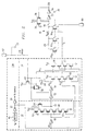
- Transistor 55 is an N-channel device, and will be on when forcing transistor 50 is in cut-off and vice-versa. Thus when output node 51 is forced to assume the value of V cc by turning transistor 50 on, no conduction path is provided between output node 51 and ground because transistor 55 is assured of being in cut-off. This occurs notwithstanding changes in the value of AS 1 .
- the signal value on output node 51 is applied to two in series inverters 52 and 54, which operate as delay elements.
- the output of inverter 54 (AS 2 ), is in turn passed to one transistor switch each in transition high detector 58 and in transition low detector 60 .
- the output of inverter 52 is applied to a pass gate 56 which functions as a noninverting delay element in parallel with inverter 54.
- the output of pass gate 56 is termed AS 3 and is also applied to one transistor each in transition high detector 58 and transition low detector 60 .
- Signals AS 0 and AS 1 are applied, respectively, to two transistors each in transition high detector 58 and transition low detector 60.
- An output signal T k from detectors 58 and 60 appears on node 67 and goes high for a period of time determined by selection of the delay values in inverters 46, 48, 52 and 54 in response to a change in state of address signal A k .
- ETD enable signal on pin 57 is high. With ETD enable high, transistor 50 is in cut-off and transistor 55 is on allowing node 51 to follow (after a delay) the value of AS 0 . Both elements of pass gate 56 are conducting and transistor 62 is off allowing AS 3 to follow AS 0 (again after delay).
- transition pulse sense elements 66 function as a NOR-gate responsive to any high going pulse on a transition sense line T going high. Any such transition turns on a pulse sense element (which are N-channel MOSFETs) thereby pulling common output node 68 low if pin 80 , a common input node for the NOR-gate array, is connected to a source of a low logic level.
- bus 68 is held high by a leakage transistor 76 connected between the input to inverter 72 and V cc .
- edge transition detector 28 One way to disable edge transition detector 28 is to tie pin 80 to V cc , which may be done by bond or mask options to provide the needed conductive lead. When pin 80 is tied to V cc bus 68 cannot be pulled low. Alternatively, fuse 70 can be opened by laser repair techniques. If this option is selected leakage transistor 76 operates to hold ETD high.
- Figure 3 is a set of timing diagrams for signals AS 0 -AS3, T k , W nor (which corresponds to the signal level on bus 68 ), the edge transition detection signal and the edge transition detection enable signal.
- edge transition detection enable is logic high and assumed to have been logic high for an indefinite prior period of time.
- AS 1 and AS 3 are logic low and signal level AS 2 is logic high.
- the transition pulse sense signal T k is low and both W nor and ETD are logic high indicating no recent transition in state for an address line.
- Edge transition detection is enabled.
- AS 0 goes logic low with a consequent change at T 2 in T k , which goes logic high and W nor which goes logic low.
- signal AS 1 goes from low to high.
Landscapes
- Engineering & Computer Science (AREA)
- Microelectronics & Electronic Packaging (AREA)
- Static Random-Access Memory (AREA)
- Dram (AREA)
Claims (5)
- Dispositif de détection de front comprenant :dans lequel le circuit logique de sommation (66) comprend en outre :un moyen générateur (30, 32, 34) agissant en réponse à un changement d'un signal d'état reçu sur une ligne de signal (Ak) pour produire un signal de transition en impulsion (Tk), caractérisé par :un tampon de sortie (38) recevant le signal de transition en impulsion (Tk) pour produire un signal de détection de front en impulsion (ETD) et comprenant un circuit logique de sommation (66) recevant une pluralité de signaux de transition en impulsion (Tk) à partir d'une pluralité de moyens (30, 32, 34) pour produire les signaux de transition en impulsion ; etun élément programmable (59, 70, 80) pour fixer le signal de détection de front en impulsion (ETD) à un niveau indiquant la non survenance d'un front ;une pluralité de transistors (66) pour recevoir un signal de transition en impulsion (Tk) sur un noeud de commande et ayant un noeud de sortie commun (WNOR) ;le noeud de sortie commun (WNOR) étant connecté à un transistor de fuite (76) pour ramener le noeud de sortie commun (WNOR) à un niveau logique prédéterminé ; etun moyen (80) pour connecter sélectivement un noeud d'entrée de chaque transistor (66) au niveau logique prédéterminé pour supprimer la génération d'une impulsion de transition de front (ETD).
- Dispositif de détection de front selon la revendication 1, dans lequel le moyen générateur (30, 32, 34) comprend :une ligne à retard (32) recevant le signal d'état sur une ligne de signal entrée (Ak) comme entrée et produisant un signal d'état retardé ; etune porte OU exclusif (34) recevant le signal d'état et le signal d'état retardé et produisant un signal de transition en impulsion.
- Dispositif de détection de front selon la revendication 1, dans lequel l'élément programmable (59, 70, 80) comprend :une ligne de validation de transition de front (ETD ENABLE) pour verrouiller la sortie du moyen (30, 32, 34) pour produire un signal de transition en impulsion à un niveau logique prédéterminé.
- Circuit intégré à mémoire statique à accès aléatoire (1) comprenant un dispositif de détection de front selon la revendication 1, et comprenant en outre :une pluralité de lignes d'adresse pour transporter les signaux d'adresse (A) ;un circuit de retard (32) connecté à chaque ligne d'adresse (A) pour produire le signal d'adresse retardé, dans lequel le moyen de génération comprend :une pluralité de circuits de comparaison (34) comprenant un premier circuit de comparaison pour chaque ligne d'adresse, chaque circuit de comparaison recevant un signal d'adresse et un signal retardé correspondant et produisant l'impulsion de transition (Tk) sur une ligne d'entrée chaque fois que le signal d'adresse et le signal d'adresse retardé correspondant ont des valeurs différentes, et une entrée de validation (ETD ENABLE) vers le circuit de comparaison.
- Circuit intégré à mémoire statique à accès aléatoire selon la revendication 4, dans lequel chaque circuit de comparaison (34) comprend en outre :une pluralité de noeuds d'entrée ; etun moyen agissant en réponse au fait que l'entrée de validation (ETD ENABLE) prend un premier niveau logique pour forcer des noeuds internes choisis à un niveau logique fixe pour invalider le dispositif de comparaison.
Applications Claiming Priority (3)
| Application Number | Priority Date | Filing Date | Title |
|---|---|---|---|
| US129763 | 1993-09-30 | ||
| US08/129,763 US5418756A (en) | 1993-09-30 | 1993-09-30 | Edge transition detection disable circuit to alter memory device operating characteristics |
| EP94307068A EP0646926B1 (fr) | 1993-09-30 | 1994-09-28 | Circuit de désactivation d'un circuit de détection de transition de flanc pour changer des caractéristiques d'opération d'un dispositif de mémoire |
Related Parent Applications (2)
| Application Number | Title | Priority Date | Filing Date |
|---|---|---|---|
| EP94307068A Division EP0646926B1 (fr) | 1993-09-30 | 1994-09-28 | Circuit de désactivation d'un circuit de détection de transition de flanc pour changer des caractéristiques d'opération d'un dispositif de mémoire |
| EP94307068.0 Division | 1994-09-28 |
Publications (3)
| Publication Number | Publication Date |
|---|---|
| EP0952549A2 EP0952549A2 (fr) | 1999-10-27 |
| EP0952549A3 EP0952549A3 (fr) | 2000-07-05 |
| EP0952549B1 true EP0952549B1 (fr) | 2002-03-06 |
Family
ID=22441484
Family Applications (2)
| Application Number | Title | Priority Date | Filing Date |
|---|---|---|---|
| EP99300541A Expired - Lifetime EP0952549B1 (fr) | 1993-09-30 | 1994-09-28 | Circuit de désactivation de la détection de transition de flanc pour changer des caractéristiques d'opération d'un dispositif de mémoire |
| EP94307068A Expired - Lifetime EP0646926B1 (fr) | 1993-09-30 | 1994-09-28 | Circuit de désactivation d'un circuit de détection de transition de flanc pour changer des caractéristiques d'opération d'un dispositif de mémoire |
Family Applications After (1)
| Application Number | Title | Priority Date | Filing Date |
|---|---|---|---|
| EP94307068A Expired - Lifetime EP0646926B1 (fr) | 1993-09-30 | 1994-09-28 | Circuit de désactivation d'un circuit de détection de transition de flanc pour changer des caractéristiques d'opération d'un dispositif de mémoire |
Country Status (4)
| Country | Link |
|---|---|
| US (1) | US5418756A (fr) |
| EP (2) | EP0952549B1 (fr) |
| JP (1) | JPH07169272A (fr) |
| DE (2) | DE69424735T2 (fr) |
Families Citing this family (10)
| Publication number | Priority date | Publication date | Assignee | Title |
|---|---|---|---|---|
| DE69413478T2 (de) * | 1993-07-30 | 1999-02-11 | Sgs-Thomson Microelectronics, Inc., Carrollton, Tex. | Inverter mit Verzögerungselement mit variabler Impedanz |
| US5602795A (en) * | 1994-01-12 | 1997-02-11 | Sun Microsystems, Inc. | Method and apparatus for implementing a high-speed dynamic line driver |
| US5469473A (en) * | 1994-04-15 | 1995-11-21 | Texas Instruments Incorporated | Transceiver circuit with transition detection |
| US5778428A (en) * | 1995-12-22 | 1998-07-07 | International Business Machines Corporation | Programmable high performance mode for multi-way associative cache/memory designs |
| US6388931B1 (en) | 1999-02-25 | 2002-05-14 | Micron Technology, Inc. | Dummy wordline for controlling the timing of the firing of sense amplifiers in a memory device in relation to the firing of wordlines in the memory device |
| US7328428B2 (en) * | 2003-09-23 | 2008-02-05 | Trivergent Technologies, Inc. | System and method for generating data validation rules |
| CN1951010A (zh) * | 2003-10-10 | 2007-04-18 | 爱特梅尔股份有限公司 | 可选择延迟的脉冲发生器 |
| US7346710B2 (en) | 2004-04-12 | 2008-03-18 | Stephen Waller Melvin | Apparatus for input/output expansion without additional control line wherein first and second signals transition directly to a different state when necessary to perform input/output |
| JP2008021340A (ja) * | 2006-07-10 | 2008-01-31 | Toshiba Microelectronics Corp | 半導体装置 |
| US7782093B2 (en) | 2007-05-23 | 2010-08-24 | Infineon Technologies Ag | Integrated circuit and method of detecting a signal edge transition |
Family Cites Families (8)
| Publication number | Priority date | Publication date | Assignee | Title |
|---|---|---|---|---|
| JPS61196498A (ja) * | 1985-02-26 | 1986-08-30 | Mitsubishi Electric Corp | 半導体記憶装置 |
| JPS634492A (ja) * | 1986-06-23 | 1988-01-09 | Mitsubishi Electric Corp | 半導体記憶装置 |
| JPS63263689A (ja) * | 1987-04-20 | 1988-10-31 | Mitsubishi Electric Corp | 半導体記憶装置 |
| KR900008554B1 (ko) * | 1988-04-23 | 1990-11-24 | 삼성전자 주식회사 | 메모리 동작모드 선택회로 |
| US4987325A (en) * | 1988-07-13 | 1991-01-22 | Samsung Electronics Co., Ltd. | Mode selecting circuit for semiconductor memory device |
| EP0419852A3 (en) * | 1989-09-22 | 1992-08-05 | Texas Instruments Incorporated | A memory with selective address transition detection for cache operation |
| US5214610A (en) * | 1989-09-22 | 1993-05-25 | Texas Instruments Incorporated | Memory with selective address transition detection for cache operation |
| JP2991479B2 (ja) * | 1990-11-16 | 1999-12-20 | 富士通株式会社 | 半導体集積回路及び半導体記憶装置 |
-
1993
- 1993-09-30 US US08/129,763 patent/US5418756A/en not_active Expired - Lifetime
-
1994
- 1994-09-28 EP EP99300541A patent/EP0952549B1/fr not_active Expired - Lifetime
- 1994-09-28 DE DE69424735T patent/DE69424735T2/de not_active Expired - Fee Related
- 1994-09-28 DE DE69430080T patent/DE69430080T2/de not_active Expired - Fee Related
- 1994-09-28 EP EP94307068A patent/EP0646926B1/fr not_active Expired - Lifetime
- 1994-09-30 JP JP6236332A patent/JPH07169272A/ja active Pending
Also Published As
| Publication number | Publication date |
|---|---|
| EP0952549A3 (fr) | 2000-07-05 |
| EP0646926A3 (fr) | 1995-11-15 |
| DE69424735D1 (de) | 2000-07-06 |
| EP0646926A2 (fr) | 1995-04-05 |
| US5418756A (en) | 1995-05-23 |
| EP0646926B1 (fr) | 2000-05-31 |
| JPH07169272A (ja) | 1995-07-04 |
| EP0952549A2 (fr) | 1999-10-27 |
| DE69430080T2 (de) | 2002-09-05 |
| DE69424735T2 (de) | 2000-11-30 |
| DE69430080D1 (de) | 2002-04-11 |
Similar Documents
| Publication | Publication Date | Title |
|---|---|---|
| US5535169A (en) | Semiconductor memory device | |
| US5923592A (en) | Fast, low power, write scheme for memory circuits using pulsed off isolation device | |
| US5506811A (en) | Dynamic memory with isolated digit lines | |
| US5412331A (en) | Word line driving circuit of a semiconductor memory device | |
| US20020000873A1 (en) | Semiconductor device having hierarchical power supply line structure improved in operating speed | |
| EP0347530B1 (fr) | Dispositif de mémoire RAM avec une fonction de réduction de consommation | |
| US6061295A (en) | Integrated circuit memory devices having time compensated column selection capability for improving write operation reliability | |
| JPH0652685A (ja) | パワーオンリセット制御型ラッチ型行ラインリピータを有する半導体メモリ | |
| US4951259A (en) | Semiconductor memory device with first and second word line drivers | |
| EP0920027B1 (fr) | Cellule de mémoire RAM à consommation réduite avec une seule ligne de bit | |
| JPH05334876A (ja) | メモリ行ライン選択用ラッチ型リピータを持った半導体メモリ | |
| US6023437A (en) | Semiconductor memory device capable of reducing a precharge time | |
| EP0952549B1 (fr) | Circuit de désactivation de la détection de transition de flanc pour changer des caractéristiques d'opération d'un dispositif de mémoire | |
| KR100242720B1 (ko) | 반도체 메모리 장치의 칼럼선택 제어회로 | |
| US5383155A (en) | Data output latch control circuit and process for semiconductor memory system | |
| US5237536A (en) | Semiconductor memory device having split operation and capable of reducing power supply noise | |
| US6166988A (en) | Semiconductor memory device using one common address bus line between address buffers and column predecoder | |
| US6677782B2 (en) | Semiconductor integrated circuit and semiconductor logic circuit used in the integrated circuit | |
| US5337273A (en) | Charge sharing flash clear for memory arrays | |
| US6741493B1 (en) | Split local and continuous bitline requiring fewer wires | |
| EP0547892B1 (fr) | Circuit intégré avec des lignes de données différentielles auto polarisées | |
| US6600342B1 (en) | Column decoder of semiconductor memory device | |
| US5257226A (en) | Integrated circuit with self-biased differential data lines | |
| US6160751A (en) | Semiconductor memory device allowing efficient column selection | |
| JP3729665B2 (ja) | 半導体装置 |
Legal Events
| Date | Code | Title | Description |
|---|---|---|---|
| PUAI | Public reference made under article 153(3) epc to a published international application that has entered the european phase |
Free format text: ORIGINAL CODE: 0009012 |
|
| AC | Divisional application: reference to earlier application |
Ref document number: 646926 Country of ref document: EP |
|
| AK | Designated contracting states |
Kind code of ref document: A2 Designated state(s): DE FR GB IT |
|
| PUAL | Search report despatched |
Free format text: ORIGINAL CODE: 0009013 |
|
| AK | Designated contracting states |
Kind code of ref document: A3 Designated state(s): DE FR GB IT |
|
| RIC1 | Information provided on ipc code assigned before grant |
Free format text: 7G 06T 7/00 A, 7G 11C 8/00 B, 7G 11C 7/22 B |
|
| 17P | Request for examination filed |
Effective date: 20001223 |
|
| GRAG | Despatch of communication of intention to grant |
Free format text: ORIGINAL CODE: EPIDOS AGRA |
|
| RIC1 | Information provided on ipc code assigned before grant |
Free format text: 7G 11C 8/00 A, 7G 11C 7/22 B |
|
| DAX | Request for extension of the european patent (deleted) | ||
| 17Q | First examination report despatched |
Effective date: 20010509 |
|
| GRAG | Despatch of communication of intention to grant |
Free format text: ORIGINAL CODE: EPIDOS AGRA |
|
| GRAG | Despatch of communication of intention to grant |
Free format text: ORIGINAL CODE: EPIDOS AGRA |
|
| GRAH | Despatch of communication of intention to grant a patent |
Free format text: ORIGINAL CODE: EPIDOS IGRA |
|
| GRAH | Despatch of communication of intention to grant a patent |
Free format text: ORIGINAL CODE: EPIDOS IGRA |
|
| REG | Reference to a national code |
Ref country code: GB Ref legal event code: IF02 |
|
| GRAA | (expected) grant |
Free format text: ORIGINAL CODE: 0009210 |
|
| AC | Divisional application: reference to earlier application |
Ref document number: 646926 Country of ref document: EP |
|
| AK | Designated contracting states |
Kind code of ref document: B1 Designated state(s): DE FR GB IT |
|
| PG25 | Lapsed in a contracting state [announced via postgrant information from national office to epo] |
Ref country code: IT Free format text: LAPSE BECAUSE OF FAILURE TO SUBMIT A TRANSLATION OF THE DESCRIPTION OR TO PAY THE FEE WITHIN THE PRESCRIBED TIME-LIMIT;WARNING: LAPSES OF ITALIAN PATENTS WITH EFFECTIVE DATE BEFORE 2007 MAY HAVE OCCURRED AT ANY TIME BEFORE 2007. THE CORRECT EFFECTIVE DATE MAY BE DIFFERENT FROM THE ONE RECORDED. Effective date: 20020306 |
|
| REF | Corresponds to: |
Ref document number: 69430080 Country of ref document: DE Date of ref document: 20020411 |
|
| ET | Fr: translation filed | ||
| PLBE | No opposition filed within time limit |
Free format text: ORIGINAL CODE: 0009261 |
|
| STAA | Information on the status of an ep patent application or granted ep patent |
Free format text: STATUS: NO OPPOSITION FILED WITHIN TIME LIMIT |
|
| 26N | No opposition filed |
Effective date: 20021209 |
|
| PG25 | Lapsed in a contracting state [announced via postgrant information from national office to epo] |
Ref country code: DE Free format text: LAPSE BECAUSE OF NON-PAYMENT OF DUE FEES Effective date: 20030401 |
|
| PG25 | Lapsed in a contracting state [announced via postgrant information from national office to epo] |
Ref country code: FR Free format text: LAPSE BECAUSE OF NON-PAYMENT OF DUE FEES Effective date: 20040528 |
|
| REG | Reference to a national code |
Ref country code: FR Ref legal event code: ST |
|
| PGFP | Annual fee paid to national office [announced via postgrant information from national office to epo] |
Ref country code: FR Payment date: 20040908 Year of fee payment: 11 |
|
| PGFP | Annual fee paid to national office [announced via postgrant information from national office to epo] |
Ref country code: GB Payment date: 20040922 Year of fee payment: 11 |
|
| REG | Reference to a national code |
Ref country code: FR Ref legal event code: D3 |
|
| PG25 | Lapsed in a contracting state [announced via postgrant information from national office to epo] |
Ref country code: GB Free format text: LAPSE BECAUSE OF NON-PAYMENT OF DUE FEES Effective date: 20050928 |
|
| GBPC | Gb: european patent ceased through non-payment of renewal fee |
Effective date: 20050928 |
|
| REG | Reference to a national code |
Ref country code: FR Ref legal event code: ST Effective date: 20060531 |